C1_Characteristic of CMOS gates_L3
- 格式:ppt
- 大小:3.61 MB
- 文档页数:65

User GuideSLUU069A - September 20001UCC3895 Phase Shift PWM ControllerEVM Kit Setup and UsagePower Supply Control Products 1IntroductionThe UCC3895 evaluation board is a 48-V input dc-to-dc converter providing 3.3 V at 15 A. It also provides 1500-V isolation between the primary and secondary portions of the circuit. This user’s guide provides the test setup and component details needed to evaluate the UCC3895evaluation board, along with some operational waveforms.This evaluation board uses the UCC3895 advanced phase shift PWM controller to implement control of a full-bridge power stage by phase-shifting the switching of one half-bridge withrespect to the other half-bridge. The circuit operates at a fixed frequency using peak currentmode control, yet promotes zero voltage switching (ZVS) over a significant portion of theconverter load range. ZVS is achieved by using the converter’s parasitic capacitance, leakage inductance, and a small discrete inductor in series with the primary winding. Additionalinformation on the full-bridge phase-shifting technique and the current-doubler rectifier can be found in references [1] - [3].This evaluation board is intended to provide an introduction to phase-shifting full-bridge power converters at a safe input voltage and power level. It is recognized that 50 W is below the typical application level of a full-bridge power supply. This topology can be used from a few hundredwatts to several kilowatts with the same basic circuit configuration.1.1FeaturesThe UCC3895 phase-shift PWM controller includes:•Programmable output turnon delay•Adaptive delay set•Bidirectional oscillator synchronization•Capability for voltage mode or current mode control•Programmable softstart and chip disable via a single pin•0% to 100% duty cycle control•7-MHz error amplifier•Operation to 1 MHz•Low active current consumption (5 mA typical @ 500 kHz)•Very low current consumption during undervoltage lockout (150 µA typical)SLUU069A1.2DescriptionThe UCC3895 provides the logic and drive signals to control the full-bridge phase shifted power supply, maintaining the functionality of the UC3875/6/7/8 and the UC3879. However, theUCC3895 improves on the previous phase shift controller families by adding features such as enhanced control logic, adaptive delay set, and shutdown capability. Since it is built inBCDMOS, it operates with dramatically less supply current than its bipolar counterparts.2SchematicA schematic of the UCC3895 evaluation board is shown in Figure 1. Terminal J2 is the inputvoltage source, J3 takes an external bias supply, and the output is taken from J1.A quick overview of the primary circuitry on the left-hand portion of the schematic shows thefull-bridge power section in the center comprised of MOFETs Q1-Q4. The control signals areprovided by U1, the UCC3895, with its accompanying circuitry. Current transformer T2 senses the primary current and provides information to the controller. PWM outputs OUTA-OUTD are buffered through driver ICs, U5 and U7, and connected to the power switching devices through gate drive transformers T3 and T4. Power is delivered to the secondary through powertransformer T1.The secondary portion of the circuit is shown on the right-hand side, and is fed from the single secondary winding of T1. This rectifier is comprised of diodes D9 and D10, output chokes L2and L3, and output capacitors C15 and C16. The output voltage is sensed through the R17-R18 divider, and a TL431 is used as an error amplifier to feed back an error signal throughoptocoupler U3. The onboard amplifier in the UCC3895 is configured as a voltage follower in this application.2UCC3895 Phase Shift PWM ControllerSLUU069A3UCC3895 Phase Shift PWM ControllerUDG –991271I N T P 25T P 24T P 23T P 22T P 21T P 20T P 19T P 18T P 17T P 16T P 15T P 14T P 13T P 12T P 11T P 10T P 9T P 8T P 7T P 6T P 5T P 4T P 3T P 2T P 1C 13J 1U 6T L 431J 3J 2C 122 n FC 2100 p FC 3C 4330 p FQ 9M M B T 3904E A +E A +D 8B A R 74D 7B A R 747864T 2C 84.7 n F D 1B A R 74D 61N 4738AC 176.8 n FC 143.3 n FC 12C 11+C 10100 VC 947 n F C 7C 6+C 5C 314.7 n FC 304.7 n F +C 16+C 15L 3L 2H S 3Q 3H S 6D 1032C T Q 030H S 5D 932C T Q 030L 1123456T 4123456T 3H S 1Q 1H S 2Q 2H S 4Q 4U 512546U 3816V C C 3G N D 71O U T 42I N252O U T U 5816V C C 3G N D 71O U T 42I N 21I N 52O U T U 71E A –2E A O3R A M P4R E F 5G N D6S Y N C7C T8R T9D E L A B10D E L C D11A D S12C S 13O U T D 14O U T C 15V C C 16P G N D 17O U T B 18O U T A 19S S /S D 20E A +U 112543T 1R 1510R 22 kR 32 kR 469.8 kR 52.4 kR 62.4 k R 7R 810R 920R 10510R 20500R 1920 kR 188.66 kR 172.8 kR 16274R 151002 WR 37102 WR 3610R 325 k R 344.7R 354.7R 335 kR 315 kR 305 k 0.1 µF2200 µF2.2 µH 2200 µF 0.1 µF2.2 µH470 µF0.47 µH0.1 µF0.1 µF1 µF1 µF47 µF o p e n Figure 1. Evaluation Board SchematicFigure 2. Zero Voltage Switching ZVS of Q2At a load current of 15 A, the circuit has an efficiency of 76.8% with Schottky rectifiers. These rectifiers were used to keep the complexity of this EVM low in order to simplify the evaluation of the UCC3895 control IC. In the lab, each Schottky was replaced with a single control-driven synchronous-rectifier (SR) MOSFET and the efficiency was measured to be 83% at 15 A.SLUU069A5UCC3895 Phase Shift PWM Controller 4Test pointsTwenty-five testpoints have been provided to monitor the significant voltage waveforms in the circuit. Their locations are given in Table 1.Test Point Designations and LocationsTEST POINTLOCATIONTP1U1 pin 3, RAMP TP2U1 pin 7, C T TP3U1 pin 20, EA+TP4U1 pin 14, OUTC TP5U1 pin 13, OUTD TP6U5 pin 7, driverA TP7U1 pin 17, OUTB TP8U1 pin 18, OUTA TP9U1 pin 5, control GND TP10U1 pin 12, CS TP11T2 pin 6, CT signal TP12Q1 source, Q2 drain TP13Power GND TP14U7 pin 5, driverD TP15U7 pin 7, driverC TP16U6 pin 3, TL431 cathode TP17Q3 source, Q4 drain TP18T1 pin 5,transformer secondary TP19V IN (–)TP20V IN (+)TP21U6 pin 1,TL431 reference TP22V OUT (–)TP23V OUT (+)TP24U6 pin 2,secondary common TP25Q2, gateSLUU069A6UCC3895 Phase Shift PWM Controller5Test setupFigure 2 shows the basic lab configuration needed to power up the UCC3895 EVM.UUTLOAD SELECTABLE3.3 V @ 15 Aor3.3 V @ 1.5 AV (0 V – 50 V)V BIAS(0–12 V)A1J 3+–J 2+–J 1++––V1TP23TP22+–+–FANIN Figure 3. Basic Lab Configuration5.1Logic Power Required (V BIAS )An external bias supply should be applied to J3 to bring the control circuitry alive before input power is applied. V BIAS should be raised above the UVLO threshold (11 V) of the UC3895, and then set at 10.5 V for optimal efficiency. With the J3 bias applied the control and switchingcircuitry can be checked from the UCC3895 outputs out to the gates of the switching MOSFETs Q1–Q4.5.2Input Source (V IN )The input voltage source applied to J2 should be capable of delivering 2 A of current to allow operation at full load. With an input of 48 V and an efficiency of approximately 75% theevaluation board draws 1.4 A with a 50-W load. Wire of 22 gauge (or larger wire diameter) can be used to make the input connections.5.3Output LoadThe output connections to J1 should be made with (2) parallel 16 gauge wires, or larger, for both the + output and the return to the load. Paralleled resistors or an electronic load can be used,with the latter enabling easier output current measurements. Using (2) parallel 16 gauge wires to run 2 feet to a load introduces a voltage drop over 100 mV, so remember to make all output voltage measurements on the PCB at TP22 and TP23. This is indicated by V1 in the diagram above.5.4FanMost power converters have power components that operate at temperatures that are high enough to cause burns if handled improperly. This evaluation board makes components accessible to allow probing of the circuit waveforms. Therefore, a small fan capable of 20–30 cfm is recommended to reduce the component temperatures with a 50-W output.SLUU069A7UCC3895 Phase Shift PWM Controller 6UCC3895-EVM part descriptionsTable 2 shows a listing of the materials used in the UCC3895 evaluation board. Specific manufacturers are not given for the generic components.UCC3895 Bill of MaterialsReferenceQty DescriptionManufacturerPart Number PCB B112-Layer, 2-oz, 8”(L)x5”(W)x0.062”(T)UCC3895 Rev. B C1122 nF, 50 V, 10%, X7R, ceramic Panasonic ECU –V1H223KBX C21100 pF, 50 V, 5% NPO, ceramic Panasonic ECU –V1H101JCG C3, C6, C11, C1240.1 µF, 50 V, 10%, X7R, ceramic Panasonic ECJ –2YB1H104K C41330 pF, 50 V, 10%, X7R, ceramic Panasonic ECU –V1H331KBN C5147 µF, 25 V, 20%, aluminum electrolytic Panasonic ECE –A1EGE470C7, C132 1 µF, 25 V, 10%, X7R, ceramic Panasonic ECJ –3YB1E105K CapacitorC8, C30, C313 4.7 nF, 50 V, 10%, X7R, ceramic Panasonic ECU –V1H472KBG C9147 nF, 100 V, 10%, X7R, ceramic Panasonic ECJ –3YB2A473K C101470 µF, 63 V, 20%, aluminum electrolytic Panasonic EEU –FA1J471L C141 3.3 nF, 50 V, 10%, X7R, ceramic Panasonic ECU –V1H332KBN C15, D1622200 µF, 6.3 V, 20%Panasonic ECA –0JFQ222C171 6.8 nF, 50 V, 10%, X7R, ceramic Panasonic ECU –V1H682KBG D1, D7, D830.15 A, 50 V, UF signal Zetex BAR74D618.2 V, 0.35 W, zener Zetex BZX84C8V2DiodeD9, D10230 A, 30 V, schottky International Rectifier 32CTQ030HS1-44Q1-Q4Aavid 592502B03400Heatsink HS5, HS62D9, D10THM THM6298B Terminal block J114-pin, 16 A, 5 mm OST ED104/4DS Terminal block J212-pin, 6 A, 5 mm OST ED350/2Header J31Single row, 2-pin, 0.1”Molex Waldom 22–03–2021Ind ctor L110.47 µH, 4 A RMS Coiltronics CTX16–14847Inductor L2, L32 2.2 µH, 25 A RMS Coiltronics HC2–2R2MOSFET Q1, Q2, Q3, Q44N-ch, 100 V, 0.058 ΩMotorola MTP33N10E TransistorQ91NPN, 40 V, 0.2 AZetexFMMT2222R1, R10, R203510 Ω, 0.1 W, 5%, surface mount Generic R2, R32 2 k Ω, 0.1 W, 5%, surface mount Generic R4169.8 k Ω, 0.1 W, 5%, surface mount Generic R5, H62 2.4 k Ω, 0.1 W, 5%, surface mount Generic ResistorR7Not usedGeneric R8110 Ω, 0.1 W, 5%, surface mount Generic R9120 Ω, 0.1 W, 5%, surface mount Generic R11Not usedGenericSLUU069A8UCC3895 Phase Shift PWM ControllerDescription Reference Qty Value/Type NumberManufacturerPart Number R151100 Ω, 0.1 W, 5%, surface mount Generic R161274 Ω, 0.1 W, 5%, surface mount Generic R171 2.8 k Ω, 0.1 W, 5%, surface mount Generic R1818.66 k Ω, 0.1 W, 5%, surface mount Generic ResistorR19120 k Ω, 0.1 W, 5%, surface mount Generic R30, R31, R32,R334 4.99 k Ω, 0.1 W, 5%, surface mount GenericR34, H352 4.7 Ω, 1 W, 5%, surface mount R36, H37210 Ω, 1 W, 5%,AxialPowertransformer T11PaytonP/N 9225 Rev C Current transformer T21GB International 3448-G Gate drive transformer T3,T42GB International 2094-MM Test pointsTP1-2525WhiteKeystone 5007U11Phase shift controller, SOIC-20Unitrode UCC3895DW U5, U72Dual driver IC, DIP-8TI TPS2812P ICU61Amp/reference, TO –92TI TL431U31Optocoupler, DIP-6VariousCNY17-2NOTES: 1.The values of these components are to be determined by the user in accordance with the application requirements.2.All resistors have tolerances of ±1%.Figure 4. Silkscreen of the UCC3895UCC3895 Phase Shift PWM ControllerFigure 5. Top Trace of the UCC3895Figure 6. Bottom Trace of the UCC3895ReferencesDesign Review: 100 W, 400 kHz, DC/DC Converter With Current Doubler Synchronous Rectification Achieves 92% Efficiency, Topic 2, SEM-1100 Power Supply Design Seminar Manual, Unitrode CorporationPhase Shifted, Zero Voltage Transition Design Considerations and the UC3875 PWM Controller Texas Instruments Application Note SLUA107The Current-Doubler Rectifier: An Alternative Rectification Technique For Push-Pull and Bridge , Texas Instruments Application Note SLUA121UCC3895 Phase Shift PWM ControllerIMPORTANT NOTICETexas Instruments and its subsidiaries (TI) reserve the right to make changes to their products or to discontinue any product or service without notice, and advise customers to obtain the latest version of relevant information to verify, before placing orders, that information being relied on is current and complete. All products are sold subject to the terms and conditions of sale supplied at the time of order acknowledgment, including those pertaining to warranty, patent infringement, and limitation of liability.TI warrants performance of its products to the specifications applicable at the time of sale in accordance with TI’s standard warranty. Testing and other quality control techniques are utilized to the extent TI deems necessary to support this warranty. Specific testing of all parameters of each device is not necessarily performed, except those mandated by government requirements.Customers are responsible for their applications using TI components.In order to minimize risks associated with the customer’s applications, adequate design and operating safeguards must be provided by the customer to minimize inherent or procedural hazards.TI assumes no liability for applications assistance or customer product design. TI does not warrant or represent that any license, either express or implied, is granted under any patent right, copyright, mask work right, or other intellectual property right of TI covering or relating to any combination, machine, or process in which such products or services might be or are used. TI’s publication of information regarding any third party’s products or services does not constitute TI’s approval, license, warranty or endorsement thereof.Reproduction of information in TI data books or data sheets is permissible only if reproduction is without alteration and is accompanied by all associated warranties, conditions, limitations and notices. Representation or reproduction of this information with alteration voids all warranties provided for an associated TI product or service, is an unfair and deceptive business practice, and TI is not responsible nor liable for any such use.Resale of TI’s products or services with statements different from or beyond the parameters stated by TI for that product or service voids all express and any implied warranties for the associated TI product or service, is an unfair and deceptive business practice, and TI is not responsible nor liable for any such use.Also see: Standard T erms and Conditions of Sale for Semiconductor Products. /sc/docs/stdterms.htmMailing Address:Texas InstrumentsPost Office Box 655303Dallas, Texas 75265Copyright © 2001, Texas Instruments Incorporated。
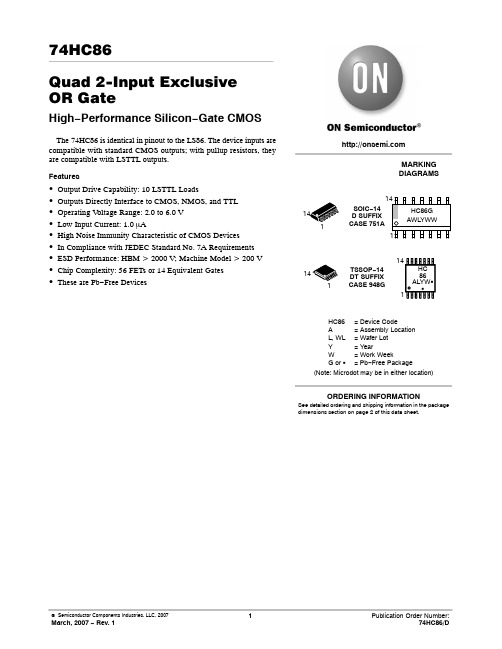
74HC86Quad 2−Input Exclusive OR GateHigh −Performance Silicon −Gate CMOSThe 74HC86 is identical in pinout to the LS86. The device inputs are compatible with standard CMOS outputs; with pullup resistors, they are compatible with LSTTL outputs.Features•Output Drive Capability: 10 LSTTL Loads•Outputs Directly Interface to CMOS, NMOS, and TTL •Operating V oltage Range: 2.0 to 6.0 V •Low Input Current: 1.0 m A•High Noise Immunity Characteristic of CMOS Devices •In Compliance with JEDEC Standard No. 7A Requirements •ESD Performance: HBM > 2000 V; Machine Model > 200 V •Chip Complexity: 56 FETs or 14 Equivalent Gates•These are Pb −Free DevicesMARKING DIAGRAMSHC86= Device CodeA = Assembly Location L, WL = Wafer Lot Y = YearW = Work WeekG or G = Pb −Free PackageTSSOP −14DT SUFFIX CASE 948G1SOIC −14D SUFFIX CASE 751AHC 86ALYW G G114See detailed ordering and shipping information in the package dimensions section on page 2 of this data sheet.ORDERING INFORMATION(Note: Microdot may be in either location)LOGIC DIAGRAMY1Y2Y3Y4A1B1A2B2A3B3A4B4PIN 14 = V CC PIN 7 = GNDY = A ⊕ B = AB + AB PIN ASSIGNMENTB3Y4A4B4V CC Y3A3A2Y1B1A1GNDY2B2FUNCTION TABLEA L L H HInputs Output B L H L HY L H H LORDERING INFORMATIONDevicePackage Shipping †74HC86DR2G SOIC −14(Pb −Free)2500 / Tape & Reel74HC86DTR2GTSSOP −14*†For information on tape and reel specifications, including part orientation and tape sizes, please refer to our Tape and Reel Packaging Specifications Brochure, BRD8011/D.*This package is inherently Pb −Free.MAXIMUM RATINGSSymbol Parameter Value Unit V CC DC Supply Voltage (Referenced to GND)– 0.5 to + 7.0V V in DC Input Voltage (Referenced to GND)– 0.5 to V CC + 0.5V V out DC Output Voltage (Referenced to GND)– 0.5 to V CC + 0.5VI in DC Input Current, per Pin±20mAI out DC Output Current, per Pin±25mAI CC DC Supply Current, V CC and GND Pins±50mAP D Power Dissipation in Still Air,SOIC Package†TSSOP Package†500450mWT stg Storage Temperature– 65 to + 150_CT L Lead Temperature, 1 mm from Case for 10 Seconds(SOIC or TSSOP Package)260_CStresses exceeding Maximum Ratings may damage the device. Maximum Ratings are stressratings only. Functional operation above the Recommended Operating Conditions is not implied.Extended exposure to stresses above the Recommended Operating Conditions may affect devicereliability.†Derating—SOIC Package: – 7 mW/_C from 65_ to 125_CTSSOP Package: − 6.1 mW/_C from 65_ to 125_CFor high frequency or heavy load considerations, see Chapter 2 of the ON Semiconductor High−Speed CMOS Data Book (DL129/D). RECOMMENDED OPERATING CONDITIONSSymbol Parameter Min Max UnitV CC DC Supply Voltage (Referenced to GND) 2.0 6.0VV in, V out DC Input Voltage, Output Voltage (Referenced toGND)0V CC VT A Operating Temperature, All Package Types– 55+ 125_Ct r, t f Input Rise and Fall Time V CC = 2.0 V (Figure 1)V CC = 4.5 VV CC = 6.0 V 01000500400nsThis device contains protectioncircuitry to guard against damagedue to high static voltages or electricfields. However, precautions mustbe taken to avoid applications of anyvoltage higher than maximum ratedvoltages to this high−impedance cir-cuit. For proper operation, V in andV out should be constrained to therange GND v (V in or V out) v V CC.Unused inputs must always betied to an appropriate logic voltagelevel (e.g., either GND or V CC).Unused outputs must be left open.DC ELECTRICAL CHARACTERISTICS (Voltages Referenced to GND)Symbol Parameter Test Conditions V CC(V)Guaranteed LimitUnit – 55 to25_C v85_C v 125_CV IH Minimum High−Level Input Voltage V out = 0.1 V or V CC – 0.1 V|I out| v 20 m A2.03.04.56.01.52.13.154.21.52.13.154.21.52.13.154.2VV IL Maximum Low−Level Input Voltage V out = 0.1 V or V CC – 0.1 V|I out| v 20 m A2.03.04.56.00.50.91.351.80.50.91.351.80.50.91.351.8VV OH Minimum High−Level Output Voltage V in = V IH or V IL|I out| v 20 m A2.04.56.01.94.45.91.94.45.91.94.45.9VV in = V IH or V IL|I out| v 2.4 mA|I out| v 4.0 mA|I out| v 5.2 mA3.04.56.02.483.985.482.343.845.342.203.705.20V OL Maximum Low−Level Output Voltage V in = V IH or V IL|I out| v 20 m A2.04.56.00.10.10.10.10.10.10.10.10.1VV in = V IH or V IL|I out| v 2.4 mA|I out| v 4.0 mA|I out| v 5.2 mA3.04.56.00.260.260.260.330.330.330.400.400.40I in Maximum Input Leakage Current V in = V CC or GND 6.0±0.1±1.0±1.0m AI CC Maximum Quiescent SupplyCurrent (per Package)V in = V CC or GNDI out = 0 m A6.0 2.02040m ANOTE:Information on typical parametric values can be found in Chapter 2 of the ON Semiconductor High−Speed CMOS Data Book (DL129/D).AC ELECTRICAL CHARACTERISTICS (C L = 50 pF, Input t, = t f = 6 ns)Symbol Parameter V CC(V)Guaranteed LimitUnit – 55 to25_C v85_C v 125_Ct PLH, t PHL Maximum Propagation Delay, Input A or B to Output Y(Figures 1 and 2)2.03.04.56.01008020171259025211501103126nst TLH, t THL Maximum Output Transition Time, Any Output(Figures 1 and 2)2.03.04.56.07530151395401916110552219nsC in Maximum Input Capacitance—101010pF NOTES:1.For propagation delays with loads other than 50 pF, see Chapter 2 of the ON Semiconductor High−Speed CMOS Data Book (DL129/D).rmation on typical parametric values can be found in Chapter 2 of the ON Semiconductor High−Speed CMOS Data Book (DL129/D).C PD Power Dissipation Capacitance (Per Gate)*Typical @ 25°C, V CC = 5.0 VpF33*Used to determine the no−load dynamic power consumption: P D = C PD V CC f + I CC V CC. For load considerations, see Chapter 2 of the ON Semiconductor High−Speed CMOS Data Book (DL129/D).*Includes all probe and jig capacitanceC L *Figure 1. Switching Waveforms Figure 2. Test CircuitGNDV CCAYFigure 3. Expanded Logic Diagram(1/4 of Device)SOIC −14CASE 751A −03ISSUE HNOTES:1.DIMENSIONING AND TOLERANCING PER ANSI Y14.5M, 1982.2.CONTROLLING DIMENSION: MILLIMETER.3.DIMENSIONS A AND B DO NOT INCLUDE MOLD PROTRUSION.4.MAXIMUM MOLD PROTRUSION 0.15 (0.006)PER SIDE.5.DIMENSION D DOES NOT INCLUDE DAMBAR PROTRUSION. ALLOWABLE DAMBAR PROTRUSION SHALL BE 0.127(0.005) TOTAL IN EXCESS OF THE D DIMENSION AT MAXIMUM MATERIAL CONDITION.DIM MIN MAX MIN MAX INCHESMILLIMETERS A 8.558.750.3370.344B 3.80 4.000.1500.157C 1.35 1.750.0540.068D 0.350.490.0140.019F 0.40 1.250.0160.049G 1.27 BSC 0.050 BSC J 0.190.250.0080.009K 0.100.250.0040.009M 0 7 0 7 P 5.80 6.200.2280.244R0.250.500.0100.019____DIMENSIONS: MILLIMETERS*For additional information on our Pb −Free strategy and soldering details, please download the ON Semiconductor Soldering and Mounting Techniques Reference Manual, SOLDERRM/D.TSSOP −14CASE 948G −01ISSUE BDIM MIN MAX MIN MAX INCHESMILLIMETERS A 4.90 5.100.1930.200B 4.30 4.500.1690.177C −−− 1.20−−−0.047D 0.050.150.0020.006F 0.500.750.0200.030G 0.65 BSC 0.026 BSC H 0.500.600.0200.024J 0.090.200.0040.008J10.090.160.0040.006K 0.190.300.0070.012K10.190.250.0070.010L 6.40 BSC 0.252 BSC M0 8 0 8 NOTES:1.DIMENSIONING AND TOLERANCING PER ANSI Y14.5M, 1982.2.CONTROLLING DIMENSION: MILLIMETER.3.DIMENSION A DOES NOT INCLUDE MOLD FLASH, PROTRUSIONS OR GATE BURRS.MOLD FLASH OR GATE BURRS SHALL NOT EXCEED 0.15 (0.006) PER SIDE.4.DIMENSION B DOES NOT INCLUDE INTERLEAD FLASH OR PROTRUSION.INTERLEAD FLASH OR PROTRUSION SHALL NOT EXCEED 0.25 (0.010) PER SIDE.5.DIMENSION K DOES NOT INCLUDE DAMBAR PROTRUSION. ALLOWABLE DAMBAR PROTRUSION SHALL BE 0.08(0.003) TOTAL IN EXCESS OF THE K DIMENSION AT MAXIMUM MATERIAL CONDITION.6.TERMINAL NUMBERS ARE SHOWN FOR REFERENCE ONLY .7.DIMENSION A AND B ARE TO BE DETERMINED AT DATUM PLANE −W −.____14X REF K14X0.360.65PITCHSOLDERING FOOTPRINT**For additional information on our Pb −Free strategy and soldering details, please download the ON Semiconductor Soldering and Mounting Techniques Reference Manual, SOLDERRM/D.ON Semiconductor and are registered trademarks of Semiconductor Components Industries, LLC (SCILLC). SCILLC reserves the right to make changes without further notice to any products herein. SCILLC makes no warranty, representation or guarantee regarding the suitability of its products for any particular purpose, nor does SCILLC assume any liability arising out of the application or use of any product or circuit, and specifically disclaims any and all liability, including without limitation special, consequential or incidental damages.“Typical” parameters which may be provided in SCILLC data sheets and/or specifications can and do vary in different applications and actual performance may vary over time. All operating parameters, including “Typicals” must be validated for each customer application by customer’s technical experts. SCILLC does not convey any license under its patent rights nor the rights of others. SCILLC products are not designed, intended, or authorized for use as components in systems intended for surgical implant into the body, or other applications intended to support or sustain life, or for any other application in which the failure of the SCILLC product could create a situation where personal injury or death may occur. Should Buyer purchase or use SCILLC products for any such unintended or unauthorized application, Buyer shall indemnify and hold SCILLC and its officers, employees, subsidiaries, affiliates, and distributors harmless against all claims, costs, damages, and expenses, and reasonable attorney fees arising out of, directly or indirectly, any claim of personal injury or death associated with such unintended or unauthorized use, even if such claim alleges that SCILLC was negligent regarding the design or manufacture of the part. SCILLC is an Equal Opportunity/Affirmative Action Employer. This literature is subject to all applicable copyright laws and is not for resale in any manner.PUBLICATION ORDERING INFORMATION。

英语介绍运河特色-回复Canals are man-made waterways that have been crucial for transportation and trade for centuries. They are designed to connect bodies of water, such as lakes or rivers, in order to provide a navigable route for ships and boats. Throughout history, canals have played a significant role in shaping the economic, cultural, and social aspects of various regions. In this article, we will explore the unique features and importance of canals, focusing on their impact on transportation, irrigation, and tourism.Transportation:One of the primary functions of canals is to facilitate transportation. By connecting different bodies of water, canals create a network that allows goods and people to be transported efficiently. In the past, canals served as vital trade routes, linking inland areas to ports and facilitating the exchange of goods between regions. The Suez Canal, for example, connects the Mediterranean Sea to the Red Sea, providing a shortcut for ships traveling between Europe and Asia. This canal has considerably reduced shipping time and costs, making it a key conduit for international trade.Irrigation:Another essential characteristic of canals is their role in irrigation. Canals have been crucial in providing water for agricultural purposes. In many regions with arid or semi-arid climates, canals enable farmers to divert water from rivers or lakes to their fields, allowing crops to grow in areas that would otherwise be unable to support agriculture. For instance, the ancient Grand Canal in China has served as a vital irrigation system for thousands of years, contributing to the country's agricultural success.Additionally, canals also play a role in flood control. By regulating the flow of water through various mechanisms such as locks and gates, canals can prevent flooding in areas prone to excessive rainfall or high water levels. This function not only protects human settlements but also helps maintain ecological balance in surrounding areas.Tourism:In recent years, canals have become popular tourist attractions worldwide. Many cities and regions have recognized the historic and aesthetic value of canals and have transformed them into recreational spaces. Places such as Venice, Amsterdam, and Bruges boast picturesque canal networks that attract millions of touristseach year.Tourists can enjoy leisurely cruises, romantic gondola rides, or explore the charming waterfronts and architectural marvels adjacent to the canals. The cultural significance of canals is often highlighted through festivals, events, and museum exhibitions, providing visitors with a glimpse into the history and heritage of the regions where the canals are situated.In conclusion, canals possess unique features and are of great importance in various aspects of human life. Their ability to connect different bodies of water makes them essential for transportation and trade. Canals also play a significant role in irrigation, enabling agricultural development in arid regions and contributing to flood control. Moreover, canals have gained popularity as tourist attractions, attracting visitors from around the world to experience their beauty and cultural significance. Overall, canals continue to shape our world and serve as an integral part of our history and future.。
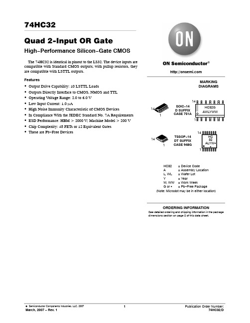
74HC32Quad 2−Input OR GateHigh−Performance Silicon−Gate CMOS The 74HC32 is identical in pinout to the LS32. The device inputs are compatible with Standard CMOS outputs; with pullup resistors, they are compatible with LSTTL outputs.Features•Output Drive Capability: 10 LSTTL Loads•Outputs Directly Interface to CMOS, NMOS and TTL •Operating V oltage Range: 2.0 to 6.0 V•Low Input Current: 1.0 m A•High Noise Immunity Characteristic of CMOS Devices•In Compliance With the JEDEC Standard No. 7A Requirements •ESD Performance: HBM > 2000 V; Machine Model > 200 V •Chip Complexity: 48 FETs or 12 Equivalent Gates•These are Pb−Free DevicesMARKINGDIAGRAMSHC32= Device CodeA= Assembly LocationL, WL= Wafer LotY= YearW, WW= Work WeekG or G= Pb−Free PackageTSSOP−14DT SUFFIXCASE 948GSOIC−14D SUFFIXCASE 751AHC32ALYW GG114See detailed ordering and shipping information in the package dimensions section on page 2 of this data sheet.ORDERING INFORMATION(Note: Microdot may be in either location)3Y11A1PIN 14 = V CC PIN 7 = GNDLOGIC DIAGRAM2B16Y24A25B28Y39A310B311Y412A413B4Y = A+BPinout: 14−Lead Packages (Top View)1314121110982134567V CC B4A4Y4B3A3Y3A1B1Y1A2B2Y2GNDL L H HL H L HFUNCTION TABLEInputs Output A B L H H HY ORDERING INFORMATIONDevicePackage Shipping †74HC32DR2G SOIC −14(Pb −Free)2500 / Tape & Reel74HC32DTR2GTSSOP −14*†For information on tape and reel specifications, including part orientation and tape sizes, please refer to our Tape and Reel Packaging Specifications Brochure, BRD8011/D.*This package is inherently Pb −Free.MAXIMUM RATINGSSymbol Parameter Value Unit V CC DC Supply Voltage (Referenced to GND)– 0.5 to + 7.0V V in DC Input Voltage (Referenced to GND)– 0.5 to V CC + 0.5V V out DC Output Voltage (Referenced to GND)– 0.5 to V CC + 0.5VI in DC Input Current, per Pin±20mAI out DC Output Current, per Pin±25mAI CC DC Supply Current, V CC and GND Pins±50mAP D Power Dissipation in Still Air,SOIC Package†TSSOP Package†500450mWT stg Storage Temperature– 65 to + 150_CT L Lead Temperature, 1 mm from Case for 10 SecondsSOIC or TSSOP Package260_CStresses exceeding Maximum Ratings may damage the device. Maximum Ratings are stressratings only. Functional operation above the Recommended Operating Conditions is not implied.Extended exposure to stresses above the Recommended Operating Conditions may affectdevice reliability.†Derating—SOIC Package: – 7 mW/_C from 65_ to 125_CTSSOP Package: − 6.1 mW/_C from 65_ to 125_CFor high frequency or heavy load considerations, see Chapter 2 of the ON Semiconductor High−Speed CMOS Data Book (DL129/D). RECOMMENDED OPERATING CONDITIONSSymbol Parameter Min Max UnitV CC DC Supply Voltage (Referenced to GND) 2.0 6.0VV in, V out DC Input Voltage, Output Voltage (Referenced toGND)0V CC VT A Operating Temperature, All Package Types– 55+ 125_Ct r, t f Input Rise and Fall Time V CC = 2.0 V (Figure 1)V CC = 4.5 VV CC = 6.0 V 01000500400nsThis device contains protectioncircuitry to guard against damagedue to high static voltages or electricfields. However, precautions mustbe taken to avoid applications of anyvoltage higher than maximum ratedvoltages to this high−impedance cir-cuit. For proper operation, V in andV out should be constrained to therange GND v (V in or V out) v V CC.Unused inputs must always betied to an appropriate logic voltagelevel (e.g., either GND or V CC).Unused outputs must be left open.DC CHARACTERISTICS(Voltages Referenced to GND)V CC (V)Guaranteed LimitSymbol Parameter Condition−55 to 25°C≤85°C≤125°C UnitV IH Minimum High−Level Input Voltage V out = 0.1V or V CC−0.1V|I out| ≤ 20m A 2.03.04.56.01.502.103.154.201.502.103.154.201.502.103.154.20VV IL Maximum Low−Level Input Voltage V out = 0.1V or V CC− 0.1V|I out| ≤ 20m A 2.03.04.56.00.500.901.351.800.500.901.351.800.500.901.351.80VV OH Minimum High−Level OutputVoltage V in = V IH or V IL|I out| ≤ 20m A2.04.56.01.94.45.91.94.45.91.94.45.9VV in =V IH or V IL|I out| ≤ 2.4mA|I out| ≤ 4.0mA|I out| ≤ 5.2mA3.04.56.02.483.985.482.343.845.342.203.705.20V OL Maximum Low−Level OutputVoltage V in = V IH or V IL|I out| ≤ 20m A2.04.56.00.10.10.10.10.10.10.10.10.1VV in = V IH or V IL|I out| ≤ 2.4mA|I out| ≤ 4.0mA|I out| ≤ 5.2mA3.04.56.00.260.260.260.330.330.330.400.400.40I in Maximum Input Leakage Current V in = V CC or GND 6.0±0.1±1.0±1.0m AI CC Maximum Quiescent SupplyCurrent (per Package)V in = V CC or GNDI out = 0m A6.0 2.02040m ANOTE:Information on typical parametric values can be found in Chapter 2 of the ON Semiconductor High−Speed CMOS Data Book (DL129/D). AC CHARACTERISTICS(C L = 50pF, Input t r = t f = 6ns)V CC (V)Guaranteed LimitSymbol Parameter−55 to 25°C≤85°C≤125°C Unitt PLH, t PHL Maximum Propagation Delay, Input A or B to Output Y(Figures 1 and 2)2.03.04.56.07530151395401916110552219nst TLH, t THL Maximum Output Transition Time, Any Output(Figures 1 and 2)2.03.04.56.07527151395321916110362219nsC in Maximum Input Capacitance101010pF NOTE:For propagation delays with loads other than 50 pF, and information on typical parametric values, see Chapter 2 of the ON Semiconductor High−Speed CMOS Data Book (DL129/D).C PD Power Dissipation Capacitance (Per Buffer)*Typical @ 25°C, V CC = 5.0 V, V EE = 0 VpF20*Used to determine the no−load dynamic power consumption: P D = C PD V CC2f + I CC V CC. For load considerations, see Chapter 2 of the ON Semiconductor High−Speed CMOS Data Book (DL129/D).Figure 1. Switching WaveformsOUTPUT YINPUT A OR BC L **Includes all probe and jig capacitanceTESTFigure 2. Test CircuitYABFigure 3. Expanded Logic Diagram(1/4 of the Device)GNDV CCSOIC −14CASE 751A −03ISSUE HNOTES:1.DIMENSIONING AND TOLERANCING PER ANSI Y14.5M, 1982.2.CONTROLLING DIMENSION: MILLIMETER.3.DIMENSIONS A AND B DO NOT INCLUDE MOLD PROTRUSION.4.MAXIMUM MOLD PROTRUSION 0.15 (0.006)PER SIDE.5.DIMENSION D DOES NOT INCLUDE DAMBAR PROTRUSION. ALLOWABLE DAMBAR PROTRUSION SHALL BE 0.127(0.005) TOTAL IN EXCESS OF THE D DIMENSION AT MAXIMUM MATERIAL CONDITION.DIM MIN MAX MIN MAX INCHESMILLIMETERS A 8.558.750.3370.344B 3.80 4.000.1500.157C 1.35 1.750.0540.068D 0.350.490.0140.019F 0.40 1.250.0160.049G 1.27 BSC 0.050 BSC J 0.190.250.0080.009K 0.100.250.0040.009M 0 7 0 7 P 5.80 6.200.2280.244R0.250.500.0100.019____DIMENSIONS: MILLIMETERS*For additional information on our Pb −Free strategy and soldering details, please download the ON Semiconductor Soldering and Mounting Techniques Reference Manual, SOLDERRM/D.TSSOP −14CASE 948G −01ISSUE BDIM MIN MAX MIN MAX INCHESMILLIMETERS A 4.90 5.100.1930.200B 4.30 4.500.1690.177C −−− 1.20−−−0.047D 0.050.150.0020.006F 0.500.750.0200.030G 0.65 BSC 0.026 BSC H 0.500.600.0200.024J 0.090.200.0040.008J10.090.160.0040.006K 0.190.300.0070.012K10.190.250.0070.010L 6.40 BSC 0.252 BSC M0 8 0 8 NOTES:1.DIMENSIONING AND TOLERANCING PER ANSI Y14.5M, 1982.2.CONTROLLING DIMENSION: MILLIMETER.3.DIMENSION A DOES NOT INCLUDE MOLD FLASH, PROTRUSIONS OR GATE BURRS.MOLD FLASH OR GATE BURRS SHALL NOT EXCEED 0.15 (0.006) PER SIDE.4.DIMENSION B DOES NOT INCLUDE INTERLEAD FLASH OR PROTRUSION.INTERLEAD FLASH OR PROTRUSION SHALL NOT EXCEED 0.25 (0.010) PER SIDE.5.DIMENSION K DOES NOT INCLUDE DAMBAR PROTRUSION. ALLOWABLE DAMBAR PROTRUSION SHALL BE 0.08(0.003) TOTAL IN EXCESS OF THE K DIMENSION AT MAXIMUM MATERIAL CONDITION.6.TERMINAL NUMBERS ARE SHOWN FOR REFERENCE ONLY .7.DIMENSION A AND B ARE TO BE DETERMINED AT DATUM PLANE −W −.____14X REF K14X0.360.65PITCHSOLDERING FOOTPRINT**For additional information on our Pb −Free strategy and soldering details, please download the ON Semiconductor Soldering and Mounting Techniques Reference Manual, SOLDERRM/D.ON Semiconductor and are registered trademarks of Semiconductor Components Industries, LLC (SCILLC). SCILLC reserves the right to make changes without further notice to any products herein. SCILLC makes no warranty, representation or guarantee regarding the suitability of its products for any particular purpose, nor does SCILLC assume any liability arising out of the application or use of any product or circuit, and specifically disclaims any and all liability, including without limitation special, consequential or incidental damages.“Typical” parameters which may be provided in SCILLC data sheets and/or specifications can and do vary in different applications and actual performance may vary over time. All operating parameters, including “Typicals” must be validated for each customer application by customer’s technical experts. SCILLC does not convey any license under its patent rights nor the rights of others. SCILLC products are not designed, intended, or authorized for use as components in systems intended for surgical implant into the body, or other applications intended to support or sustain life, or for any other application in which the failure of the SCILLC product could create a situation where personal injury or death may occur. Should Buyer purchase or use SCILLC products for any such unintended or unauthorized application, Buyer shall indemnify and hold SCILLC and its officers, employees, subsidiaries, affiliates, and distributors harmless against all claims, costs, damages, and expenses, and reasonable attorney fees arising out of, directly or indirectly, any claim of personal injury or death associated with such unintended or unauthorized use, even if such claim alleges that SCILLC was negligent regarding the design or manufacture of the part. SCILLC is an Equal Opportunity/Affirmative Action Employer. This literature is subject to all applicable copyright laws and is not for resale in any manner.PUBLICATION ORDERING INFORMATION。
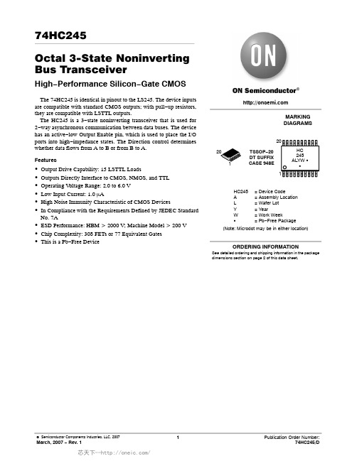
74HC245Octal 3−State Noninverting Bus TransceiverHigh −Performance Silicon −Gate CMOSThe 74HC245 is identical in pinout to the LS245. The device inputs are compatible with standard CMOS outputs; with pull −up resistors,they are compatible with LSTTL outputs.The HC245 is a 3−state noninverting transceiver that is used for 2−way asynchronous communication between data buses. The device has an active −low Output Enable pin, which is used to place the I/O ports into high −impedance states. The Direction control determines whether data flows from A to B or from B to A.Features•Output Drive Capability: 15 LSTTL Loads•Outputs Directly Interface to CMOS, NMOS, and TTL •Operating V oltage Range: 2.0 to 6.0 V •Low Input Current: 1.0 m A•High Noise Immunity Characteristic of CMOS Devices•In Compliance with the Requirements Defined by JEDEC Standard No. 7A•ESD Performance: HBM > 2000 V; Machine Model > 200 V•Chip Complexity: 308 FETs or 77 Equivalent Gates •This is a Pb −Free Device120MARKING DIAGRAMSHC 245ALYW GGTSSOP −20DT SUFFIX CASE 948ESee detailed ordering and shipping information in the package dimensions section on page 2 of this data sheet.ORDERING INFORMATIONHC245= Device CodeA = Assembly Location L = Wafer Lot Y = YearW = Work WeekG = Pb −Free Package(Note: Microdot may be in either location)Figure 1. Pin Assignment A5A3A2A1DIRECTIONGNDA8A7A6A4B3B2B1OUTPUT ENABLE V CCB8B7B6B5B4A DATA PORTA8A7A6A5A3A4A2A1DIRECTION OUTPUT ENABLEPIN 10 = GND PIN 20 = V CCB1B2B3B4B5B6B7B8B DATA PORTFigure 2. Logic DiagramFUNCTION TABLEControl Inputs OperationOutput Enable DirectionL L Data Transmitted from Bus B to Bus A L H Data Transmitted from Bus A to Bus B H XBuses Isolated (High −Impedance State)X = don’t careORDERING INFORMATIONDevicePackage Shipping †74HC245DTR2GTSSOP −20*2500 / Tape & Reel†For information on tape and reel specifications, including part orientation and tape sizes, please refer to our Tape and Reel Packaging Specifications Brochure, BRD8011/D.*This package is inherently Pb −Free.MAXIMUM RATINGS (Note 1)Symbol Parameter Value Unit V CC DC Supply Voltage*0.5 to )7.0V V IN DC Input Voltage*0.5 to V CC)0.5V V OUT DC Output Voltage(Note 2)*0.5 to V CC)0.5VI IK DC Input Diode Current$20mAI OK DC Output Diode Current$35mA I OUT DC Output Sink Current$35mAI CC DC Supply Current per Supply Pin$75mA I GND DC Ground Current per Ground Pin$75mA T STG Storage Temperature Range*65 to )150_C T L Lead Temperature, 1 mm from Case for 10 Seconds260_C T J Junction Temperature Under Bias)150_C q JA Thermal Resistance TSSOP128_C/W P D Power Dissipation in Still Air at 85_C TSSOP450mW MSL Moisture Sensitivity Level 1F R Flammability Rating Oxygen Index: 30% to 35%UL 94 V−0 @ 0.125 inV ESD ESD Withstand Voltage Human Body Model (Note 3)Machine Model (Note 4)u2000u200VI LATCHUP Latchup Performance Above V CC and Below GND at 85_C (Note 5)$300mA Stresses exceeding Maximum Ratings may damage the device. Maximum Ratings are stress ratings only. Functional operation above theRecommended Operating Conditions is not implied. Extended exposure to stresses above the Recommended Operating Conditions may affect device reliability.1.Measured with minimum pad spacing on an FR4 board, using 10 mm−by−1 inch, 20 ounce copper trace with no air flow.2.I O absolute maximum rating must observed.3.Tested to EIA/JESD22−A114−A.4.Tested to EIA/JESD22−A115−A.5.Tested to EIA/JESD78.RECOMMENDED OPERATING CONDITIONSSymbol Parameter Min Max Unit V CC DC Supply Voltage (Referenced to GND) 2.0 6.0VV in, V out DC Input Voltage, Output Voltage (Referenced to GND)0V CC V T A Operating Temperature, All Package Types–55+125_Ct r, t f Input Rise and Fall Time V CC = 2.0 V (Figure 3)V CC = 4.5 VV CC = 6.0 V 01000500400nsDC ELECTRICAL CHARACTERISTICS (Voltages Referenced to GND)Guaranteed LimitSymbol Parameter Test Conditions V CCV–55 to25_C v 85_C v 125_C UnitV IH Minimum High−Level Input Voltage V out = V CC – 0.1 V|I out| v 20 m A 2.03.04.56.01.52.13.154.21.52.13.154.21.52.13.154.2VV IL Maximum Low−Level Input Voltage V out = 0.1 V|I out| v 20 m A 2.03.04.56.00.50.91.351.80.50.91.351.80.50.91.351.8VV OH Minimum High−Level Output Voltage V in = V IH|I out| v 20 m A2.04.56.01.94.45.91.94.45.91.94.45.9VV in = V IH|I out| v 2.4 mA|I out| v 6.0 mA|I out| v 7.8 mA3.04.56.02.483.985.482.343.845.342.23.75.2V OL Maximum Low−Level Output Voltage V in = V IL|I out| v 20 m A2.04.56.00.10.10.10.10.10.10.10.10.1VV in = V IL|I out| v 2.4 mA|I out| v 6.0 mA|I out| v 7.8 mA3.04.56.00.260.260.260.330.330.330.40.40.4I in Maximum Input Leakage Current V in = V CC or GND 6.0±0.1±1.0±1.0m AI OZ Maximum Three−State LeakageCurrent Output in High−Impedance StateV in = V IL or V IHV out = V CC or GND6.0±0.5±5.0±10m AI CC Maximum Quiescent SupplyCurrent (per Package)V in = V CC or GNDI out = 0 m A6.0 4.04040m Armation on typical parametric values and high frequency or heavy load considerations can be found in the ON SemiconductorHigh−Speed CMOS Data Book (DL129/D).AC ELECTRICAL CHARACTERISTICS (C L = 50 pF, Input t r = t f = 6 ns)Symbol Parameter V CCVGuaranteed LimitUnit –55 to25_C v85_C v 125_Ct PLH, t PHL Maximum Propagation Delay,A to B,B to A(Figures 1 and 3)2.03.04.56.07555151395701916110802219nst PLZ, t PHZ Maximum Propagation Delay,Direction or Output Enable to A or B(Figures 2 and 4)2.03.04.56.011090221914011028241651303328nst PZL, t PZH Maximum Propagation Delay,Output Enable to A or B(Figures 2 and 4)2.03.04.56.011090221914011028241651303328nst TLH, t THL Maximum Output Transition Time,Any Output(Figures 1 and 3)2.03.04.56.0602312107527151390321815nsC in Maximum Input Capacitance (Pin 1 or Pin 19)−101010pFC out Maximum Three−State I/O Capacitance(I/O in High−Impedance State)−151515pF7.For propagation delays with loads other than 50 pF, and information on typical parametric values, see the ON Semiconductor High−SpeedCMOS Data Book (DL129/D).C PD Power Dissipation Capacitance (Per Transceiver Channel) (Note 8)Typical @ 25°C, V CC = 5.0 VpF40ed to determine the no−load dynamic power consumption: P D = C PD V CC f + I CC V CC. For load considerations, see the ONSemiconductor High−Speed CMOS Data Book (DL129/D).V CCGNDFigure 3. Switching Waveform OUTPUT ENABLE A OR B A OR BV CCGNDHIGHIMPEDANCEV OLV OHHIGHIMPEDANCEV CCGNDFigure 4. Switching WaveformDIRECTION*Includes all probe and jig capacitanceC L*TEST POINTFigure 5. Test Circuit*Includes all probe and jig capacitanceTEST POINTFigure 6. Test CircuitCONNECT TO V CC WHENTESTING t PLZ AND t PZL.CONNECT TO GND WHENTESTING t PHZ AND t PZH.A DATA PORTBDATAPORTB1B2B3B4B5B6B7B8Figure 7. Expanded Logic DiagramPACKAGE DIMENSIONSTSSOP −20CASE 948E −02ISSUE CDIM A MIN MAX MIN MAX INCHES 6.600.260MILLIMETERS B 4.30 4.500.1690.177C 1.200.047D 0.050.150.0020.006F 0.500.750.0200.030G 0.65 BSC 0.026 BSC H 0.270.370.0110.015J 0.090.200.0040.008J10.090.160.0040.006K 0.190.300.0070.012K10.190.250.0070.010L 6.40 BSC 0.252 BSCM0 8 0 8 ____NOTES:1.DIMENSIONING AND TOLERANCING PER ANSI Y14.5M, 1982.2.CONTROLLING DIMENSION:MILLIMETER.3.DIMENSION A DOES NOT INCLUDE MOLD FLASH, PROTRUSIONS OR GATE BURRS. MOLD FLASH OR GATE BURRS SHALL NOT EXCEED 0.15 (0.006) PER SIDE.4.DIMENSION B DOES NOT INCLUDE INTERLEAD FLASH OR PROTRUSION.INTERLEAD FLASH OR PROTRUSIONSHALL NOT EXCEED 0.25 (0.010) PER SIDE.5.DIMENSION K DOES NOT INCLUDE DAMBAR PROTRUSION. ALLOWABLE DAMBAR PROTRUSION SHALL BE 0.08(0.003) TOTAL IN EXCESS OF THE K DIMENSION AT MAXIMUM MATERIAL CONDITION.6.TERMINAL NUMBERS ARE SHOWN FOR REFERENCE ONLY .7.DIMENSION A AND B ARE TO BE DETERMINED AT DATUM PLANE −W −.6.400.252−−−−−−16X0.360.65PITCHSOLDERING FOOTPRINT**For additional information on our Pb −Free strategy and soldering details, please download the ON Semiconductor Soldering and Mounting Techniques Reference Manual, SOLDERRM/D.ON Semiconductor and are registered trademarks of Semiconductor Components Industries, LLC (SCILLC). SCILLC reserves the right to make changes without further notice to any products herein. SCILLC makes no warranty, representation or guarantee regarding the suitability of its products for any particular purpose, nor does SCILLC assume any liability arising out of the application or use of any product or circuit, and specifically disclaims any and all liability, including without limitation special, consequential or incidental damages.“Typical” parameters which may be provided in SCILLC data sheets and/or specifications can and do vary in different applications and actual performance may vary over time. All operating parameters, including “Typicals” must be validated for each customer application by customer’s technical experts. SCILLC does not convey any license under its patent rights nor the rights of others. SCILLC products are not designed, intended, or authorized for use as components in systems intended for surgical implant into the body, or other applications intended to support or sustain life, or for any other application in which the failure of the SCILLC product could create a situation where personal injury or death may occur. Should Buyer purchase or use SCILLC products for any such unintended or unauthorized application, Buyer shall indemnify and hold SCILLC and its officers, employees, subsidiaries, affiliates, and distributors harmless against all claims, costs, damages, and expenses, and reasonable attorney fees arising out of, directly or indirectly, any claim of personal injury or death associated with such unintended or unauthorized use, even if such claim alleges that SCILLC was negligent regarding the design or manufacture of the part. SCILLC is an Equal Opportunity/Affirmative Action Employer. This literature is subject to all applicable copyright laws and is not for resale in any manner.PUBLICATION ORDERING INFORMATION。
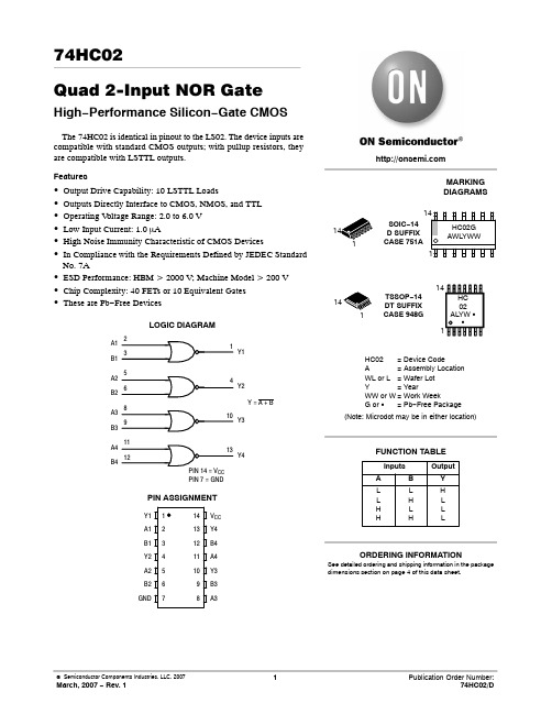
74HC02Quad 2−Input NOR GateHigh−Performance Silicon−Gate CMOS The 74HC02 is identical in pinout to the LS02. The device inputs are compatible with standard CMOS outputs; with pullup resistors, they are compatible with LSTTL outputs.Features•Output Drive Capability: 10 LSTTL Loads•Outputs Directly Interface to CMOS, NMOS, and TTL •Operating V oltage Range: 2.0 to 6.0 V•Low Input Current: 1.0 m A•High Noise Immunity Characteristic of CMOS Devices•In Compliance with the Requirements Defined by JEDEC Standard No. 7A•ESD Performance: HBM > 2000 V; Machine Model > 200 V •Chip Complexity: 40 FETs or 10 Equivalent Gates•These are Pb−Free DevicesLOGIC DIAGRAMY1A1CCPIN 7 = GNDB1Y4Y = A + BY2A2B2Y3A3B3A4B4PIN ASSIGNMENTY3A4B4Y4V CCA3B3Y2B1A1Y1GNDB2A2See detailed ordering and shipping information in the packagedimensions section on page 4 of this data sheet.ORDERING INFORMATIONMAXIMUM RATINGSSymbol Parameter Value Unit V CC DC Supply Voltage (Referenced to GND)– 0.5 to + 7.0V V in DC Input Voltage (Referenced to GND)– 0.5 to V CC + 0.5V V out DC Output Voltage (Referenced to GND)– 0.5 to V CC + 0.5VI in DC Input Current, per Pin±20mAI out DC Output Current, per Pin±25mAI CC DC Supply Current, V CC and GND Pins±50mAP D Power Dissipation in Still Air,SOIC Package†TSSOP Package†500450mWT stg Storage Temperature– 65 to + 150_CT L Lead Temperature, 1 mm from Case for 10 SecondsSOIC or TSSOP Package260_CStresses exceeding Maximum Ratings may damage the device. Maximum Ratings are stressratings only. Functional operation above the Recommended Operating Conditions is not im-plied. Extended exposure to stresses above the Recommended Operating Conditions may af-fect device reliability.†Derating—SOIC Package: – 7 mW/_C from 65_ to 125_CTSSOP Package: − 6.1 mW/_C from 65_ to 125_CFor high frequency or heavy load considerations, see Chapter 2 of the ON Semiconductor High−Speed CMOS Data Book (DL129/D). RECOMMENDED OPERATING CONDITIONSSymbol Parameter Min Max UnitV CC DC Supply Voltage (Referenced to GND) 2.0 6.0VV in, V out DC Input Voltage, Output Voltage (Referenced to GND)0V CC VT A Operating Temperature, All Package Types– 55+ 125_Ct r, t f Input Rise and Fall Time V CC = 2.0 V (Figure 1)V CC = 4.5 VV CC = 6.0 V 01000500400nsThis device contains protectioncircuitry to guard against damagedue to high static voltages or electricfields. However, precautions mustbe taken to avoid applications of anyvoltage higher than maximum ratedvoltages to this high−impedance cir-cuit. For proper operation, V in andV out should be constrained to therange GND v (V in or V out) v V CC.Unused inputs must always betied to an appropriate logic voltagelevel (e.g., either GND or V CC).Unused outputs must be left open.DC ELECTRICAL CHARACTERISTICS (Voltages Referenced to GND)Guaranteed LimitSymbol Parameter Test Conditions V CC(V)– 55 to25_C v85_C v125°C UnitV IH Minimum High−Level InputVoltage V out = 0.1 V or V CC – 0.1 V|I out| v 20 m A2.03.04.56.01.52.13.154.21.52.13.154.21.52.13.154.2VV IL Maximum Low−Level InputVoltage V out = 0.1 V or V CC – 0.1 V|I out| v 20 m A2.03.04.56.00.50.91.351.80.50.91.351.80.50.91.351.8VV OH Minimum High−Level OutputVoltage V in = V IH or V IL|I out| v 20 m A2.04.56.01.94.45.91.94.45.91.94.45.9VV in = V IH or V IL|I out| v 2.4 mA|I out| v 4.0 mA|I out| v 5.2 mA3.04.56.02.483.985.482.343.845.342.203.75.2V OL Maximum Low−Level OutputVoltage V in = V IH or V IL|I out| v 20 m A2.04.56.00.10.10.10.10.10.10.10.10.1VV in = V IH or V IL|I out| v 2.4 mA|I out| v 4.0 mA|I out| v 5.2 mA3.04.56.00.260.260.260.330.330.330.40.40.4I in Maximum Input LeakageCurrentV in = V CC or GND 6.0±0.1±1.0±1.0m AI CC Maximum Quiescent SupplyCurrent (per Package)V in = V CC or GND|I out| = 0 m A6.0 2.02040m ANOTE:Information on typical parametric values can be found in Chapter 2 of the ON Semiconductor High−Speed CMOS Data Book (DL129/D).AC ELECTRICAL CHARACTERISTICS (C L = 50 pF, Input t r = t f= 6.0 ns)Guaranteed LimitSymbol Parameter V CC(V)– 55 to25_C v85_C v125_C Unitt PLH, t PHL Maximum Propagation Delay, Input A or B to Output Y(Figures 1 and 2)2.03.04.56.07530151395401916110552219nst TLH, t THL Maximum Output Transition Time, Any Output(Figures 1 and 2)2.03.04.56.07530151395401916110552219nsC in Maximum Input Capacitance—101010pF NOTE:For propagation delays with loads other than 50 pF, and information on typical parametric values, see Chapter 2 of the ON Semiconductor High−Speed CMOS Data Book (DL129/D).C PD Power Dissipation Capacitance (Per Gate)*Typical @ 25°C, V CC = 5.0 VpF22*Used to determine the no−load dynamic power consumption: P D = C PD V CC2f + I CC V CC. For load considerations, see Chapter 2 of the ON Semiconductor High−Speed CMOS Data Book (DL129/D).ORDERING INFORMATIONDevicePackage Shipping †74HC02DR2G SOIC −14(Pb −Free)2500/Tape & Reel74HC02DTR2GTSSOP −14*†For information on tape and reel specifications, including part orientation and tape sizes, please refer to our Tape and Reel Packaging Specifications Brochure, BRD8011/D.*This package is inherently Pb −Free.Figure 1. Switching Waveforms V CC GNDINPUT A OR BOUTPUT Y*Includes all probe and jig capacitanceFigure 2. Test CircuitC L *YABFigure 3. Expanded Logic Diagram(1/4 of the Device)SOIC −14CASE 751A −03ISSUE HNOTES:1.DIMENSIONING AND TOLERANCING PER ANSI Y14.5M, 1982.2.CONTROLLING DIMENSION: MILLIMETER.3.DIMENSIONS A AND B DO NOT INCLUDE MOLD PROTRUSION.4.MAXIMUM MOLD PROTRUSION 0.15 (0.006)PER SIDE.5.DIMENSION D DOES NOT INCLUDE DAMBAR PROTRUSION. ALLOWABLE DAMBAR PROTRUSION SHALL BE 0.127(0.005) TOTAL IN EXCESS OF THE D DIMENSION AT MAXIMUM MATERIAL CONDITION.DIM MIN MAX MIN MAX INCHESMILLIMETERS A 8.558.750.3370.344B 3.80 4.000.1500.157C 1.35 1.750.0540.068D 0.350.490.0140.019F 0.40 1.250.0160.049G 1.27 BSC 0.050 BSC J 0.190.250.0080.009K 0.100.250.0040.009M 0 7 0 7 P 5.80 6.200.2280.244R0.250.500.0100.019____DIMENSIONS: MILLIMETERS*For additional information on our Pb −Free strategy and soldering details, please download the ON Semiconductor Soldering and Mounting Techniques Reference Manual, SOLDERRM/D.TSSOP −14CASE 948G −01ISSUE BDIM MIN MAX MIN MAX INCHESMILLIMETERS A 4.90 5.100.1930.200B 4.30 4.500.1690.177C −−− 1.20−−−0.047D 0.050.150.0020.006F 0.500.750.0200.030G 0.65 BSC 0.026 BSC H 0.500.600.0200.024J 0.090.200.0040.008J10.090.160.0040.006K 0.190.300.0070.012K10.190.250.0070.010L 6.40 BSC 0.252 BSC M0 8 0 8 NOTES:1.DIMENSIONING AND TOLERANCING PER ANSI Y14.5M, 1982.2.CONTROLLING DIMENSION: MILLIMETER.3.DIMENSION A DOES NOT INCLUDE MOLD FLASH, PROTRUSIONS OR GATE BURRS.MOLD FLASH OR GATE BURRS SHALL NOT EXCEED 0.15 (0.006) PER SIDE.4.DIMENSION B DOES NOT INCLUDE INTERLEAD FLASH OR PROTRUSION.INTERLEAD FLASH OR PROTRUSION SHALL NOT EXCEED 0.25 (0.010) PER SIDE.5.DIMENSION K DOES NOT INCLUDE DAMBAR PROTRUSION. ALLOWABLE DAMBAR PROTRUSION SHALL BE 0.08(0.003) TOTAL IN EXCESS OF THE K DIMENSION AT MAXIMUM MATERIAL CONDITION.6.TERMINAL NUMBERS ARE SHOWN FOR REFERENCE ONLY .7.DIMENSION A AND B ARE TO BE DETERMINED AT DATUM PLANE −W −.____14X REF K14X0.360.65PITCHSOLDERING FOOTPRINT**For additional information on our Pb −Free strategy and soldering details, please download the ON Semiconductor Soldering and Mounting Techniques Reference Manual, SOLDERRM/D.ON Semiconductor and are registered trademarks of Semiconductor Components Industries, LLC (SCILLC). SCILLC reserves the right to make changes without further notice to any products herein. SCILLC makes no warranty, representation or guarantee regarding the suitability of its products for any particular purpose, nor does SCILLC assume any liability arising out of the application or use of any product or circuit, and specifically disclaims any and all liability, including without limitation special, consequential or incidental damages.“Typical” parameters which may be provided in SCILLC data sheets and/or specifications can and do vary in different applications and actual performance may vary over time. All operating parameters, including “Typicals” must be validated for each customer application by customer’s technical experts. SCILLC does not convey any license under its patent rights nor the rights of others. SCILLC products are not designed, intended, or authorized for use as components in systems intended for surgical implant into the body, or other applications intended to support or sustain life, or for any other application in which the failure of the SCILLC product could create a situation where personal injury or death may occur. Should Buyer purchase or use SCILLC products for any such unintended or unauthorized application, Buyer shall indemnify and hold SCILLC and its officers, employees, subsidiaries, affiliates, and distributors harmless against all claims, costs, damages, and expenses, and reasonable attorney fees arising out of, directly or indirectly, any claim of personal injury or death associated with such unintended or unauthorized use, even if such claim alleges that SCILLC was negligent regarding the design or manufacture of the part. SCILLC is an Equal Opportunity/Affirmative Action Employer. This literature is subject to all applicable copyright laws and is not for resale in any manner.PUBLICATION ORDERING INFORMATION。
MC74HC161A,MC74HC163APresettable CountersHigh−Performance Silicon−Gate CMOSThe MC74HC161A and HC163A are identical in pinout to the LS161 and LS163. The device inputs are compatible with standard CMOS outputs; with pullup resistors, they are compatible with LSTTL outputs.The HC161A and HC163A are programmable 4−bit binary counters with asynchronous and synchronous reset, respectively.Features•Output Drive Capability: 10 LSTTL Loads•Outputs Directly Interface to CMOS, NMOS, and TTL •Operating V oltage Range: 2.0 to 6.0 V•Low Input Current: 1.0 m A•High Noise Immunity Characteristic of CMOS Devices•In Compliance with the Requirements Defined by JEDEC Standard No. 7A•Chip Complexity: 192 FETs or 48 Equivalent Gates•Pb−Free Packages are Available**For additional information on our Pb−Free strategy and soldering details, please download the ON Semiconductor Soldering and Mounting Techniques Reference Manual, SOLDERRM/D.MARKINGDIAGRAMSSOIC−16D SUFFIXCASE 751BTSSOP−16DT SUFFIXCASE 948FPDIP−16N SUFFIXCASE 648116MC74HC16xANAWLYYWWG116HC16xAGAWLYWWHC16xAALYW GG116x= 1 or 3A=Assembly LocationWL, L=Wafer LotYY, Y=YearWW, W=Work WeekG or G= Pb−Free PackageSee detailed ordering and shipping information in the package dimensions section on page 13 of this data sheet.ORDERING INFORMATION(Note: Microdot may be in either location)InputsOutput ClockReset*Load Enable PEnable TQL X X X ResetH L X X Load Preset DataH H H H Count H H L X No Count HHXLNo CountFUNCTION TABLE*HC163A only. HC161A is an Asynchronous Reset Device H = high level, L = low level, X = don’t careFigure 1. Pin AssignmentRESET P0CLOCKGNDQ1Q0RIPPLECARRY OUT V CCP1P2P3ENABLE PQ2Q3ENABLE T LOADFigure 2. Logic DiagramCC Q0Q1Q2Q3RIPPLE CARRY OUTBCD OR BINARY OUTPUTP0P1P2P3CLOCKCOUNT ENABLESPRESET DATA INPUTSDEVICE/MODE TABLEDevice Count Mode Reset Mode HC161A Binary Asynchronous HC163ABinarySynchronousMAXIMUM RATINGSSymbol Parameter Value Unit V CC DC Supply Voltage*0.5 to )7.0V V I DC Input Voltage*0.5 to V CC)0.5V V O DC Output Voltage(Note 1)*0.5 v V O v V CC)0.5VI IK DC Input Diode Current$20mAI OK DC Output Diode Current$25mAI O DC Output Sink Current$25mAI CC DC Supply Current per Supply Pin$50mA I GND DC Ground Current per Ground Pin$50mA T STG Storage Temperature Range*65 to )150_C T L Lead Temperature, 1 mm from Case for 10 Seconds260_C T J Junction Temperature Under Bias)150_Cq JA Thermal Resistance PDIPSOICTSSOP 78112148_C/WP D Power Dissipation in Still Air at 85_C PDIPSOICTSSOP 750500450mWMSL Moisture Sensitivity Level 1F R Flammability Rating Oxygen Index: 30% − 35%UL 94 V−0 @ 0.125 inV ESD ESD Withstand Voltage Human Body Model (Note 2)Machine Model (Note 3)u2000u200VI LATCHUP Latchup Performance Above V CC and Below GND at 85_C (Note 4)$300mA Stresses exceeding Maximum Ratings may damage the device. Maximum Ratings are stress ratings only. Functional operation above theRecommended Operating Conditions is not implied. Extended exposure to stresses above the Recommended Operating Conditions may affect device reliability.1.I O absolute maximum rating must be observed.2.Tested to EIA/JESD22−A114−A.3.Tested to EIA/JESD22−A115−A.4.Tested to EIA/JESD78.RECOMMENDED OPERATING CONDITIONSSymbol Parameter Min Max Unit V CC DC Supply Voltage(Referenced to GND) 2.0 6.0VV in, V out DC Input Voltage, Output Voltage(Referenced to GND)0V CC V T A Operating Temperature, All Package Types*55)125_Ct r, t f Input Rise and Fall Time (Figure 4)V CC = 2.0 VV CC = 3.0 VV CC = 4.5 VV CC = 6.0 V 01000600500400ns5.Unused inputs may not be left open. All inputs must be tied to a high− or low−logic input voltage level.DC ELECTRICAL CHARACTERISTICS (Voltages Referenced to GND)Symbol Parameter Test Conditions V CCVGuaranteed LimitUnit –55 to 25_C v85_C v 125_CV IH Minimum High−LevelInput Voltage V out = 0.1 V or V CC – 0.1 V|I out| v 20 m A2.03.04.56.01.52.13.154.21.52.13.154.21.52.13.154.2VV IL Maximum Low−LevelInput Voltage V out = 0.1 V or V CC – 0.1 V|I out| v 20 m A2.03.04.56.00.50.91.351.80.50.91.351.80.50.91.351.8VV OH Minimum High−LevelOutput Voltage V in = V IH or V IL|I out| v 20 m A2.04.56.01.94.45.91.94.45.91.94.45.9VV in = V IH or V IL|I out| v 3.6 mA|I out| v 4.0 mA|I out| v 5.2 mA3.04.56.02.483.985.482.343.845.342.23.75.2V OL Maximum Low−LevelOutput Voltage V in = V IH or V IL|I out| v 20 m A2.04.56.00.10.10.10.10.10.10.10.10.1VV in = V IH or V IL|I out| v 3.6 mA|I out| v 4.0 mA|I out| v 5.2 mA3.04.56.00.260.260.260.330.330.330.40.40.4I in Maximum InputLeakage CurrentV in = V CC or GND 6.0±0.1±1.0±1.0m AI CC Maximum QuiescentSupply Current V in = V CC or GNDI out = 0 m A6.0 4.040160m AAC ELECTRICAL CHARACTERISTICS (C L = 50 pF, Input t r = t f = 6.0 ns)Symbol Parameter Figure V CCVGuaranteed LimitUnit – 55 to 25_C v85_C v 125_Cf max Maximum Clock Frequency(50% Duty Cycle)(Note 6)4, 10 2.03.04.56.0615303551224284102024MHzt PLH Maximum Propagation Delay, Clock to Q 4, 10 2.03.04.56.012075201616012023202001502822nst PHL4, 10 2.03.04.56.0145100221818513525202201503023nst PHL Maximum Propagation Delay, Reset to Q (HC161A Only)5, 10 2.03.04.56.0145100201718513522192201502521nst PLH Maximum Propagation Delay, Enable T to Ripple Carry Out 6, 10 2.03.04.56.011060161415011518151901402017nst PHL6, 10 2.03.04.56.0135100181517513020162101602220nst PLH Maximum Propagation Delay, Clock to Ripple Carry Out 4, 10 2.03.04.56.012075221816013527222001503025nst PHL4, 10 2.03.04.56.0145100222018513528242201503528nst PHL Maximum Propagation Delay, Reset to Ripple Carry Out(HC161A Only)5, 10 2.03.04.56.0155120221819014026222301553025nst TLH, t THL Maximum Output Transition Time,Any Output5, 10 2.03.04.56.07530151395401916110552219nsC in Maximum Input Capacitance4, 10−101010pF6.Applies to noncascaded/nonsynchronous clocked configurations only with synchronously cascaded counters. (1) Clock to Ripple Carry Outpropagation delays. (2) Enable T or Enable P to Clock setup times and (3) Clock to Enable T or Enable P hold times determine f max. However, if Ripple Carry out of each stage is tied to the Clock of the next stage (nonsynchronously clocked) the f max in the table above is applicable.See Applications information in this data sheet.C PD Power Dissipation Capacitance (Per Gate) (Note 7)Typical @ 25°C, V CC = 5.0 VpF45ed to determine the no−load dynamic power consumption: P D = C PD V CC f + I CC V CC.TIMING REQUIREMENTS (C L = 50 pF, Input t r = t f = 6.0 ns)Symbol Parameter Figure V CCVGuaranteed LimitUnit – 55 to 25_C v85_C v 125_Ct su Minimum Setup Time,Preset Data Inputs to Clock 8 2.03.04.56.0402015126030201880403020nst su Minimum Setup Time,Load to Clock 8 2.03.04.56.0602515127530201890403020nst su Minimum Setup Time,Reset to Clock (HC163A Only)7 2.03.04.56.0602520177530252390403525nst su Minimum Setup Time,Enable T or Enable P to Clock 9 2.03.04.56.08035201795402523110503525nst h Minimum Hold Time,Clock to Load or Preset Data Inputs 8 2.03.04.56.0333333333333nst h Minimum Hold Time,Clock to Reset (HC163A Only)7 2.03.04.56.0333333333333nst h Minimum Hold Time,Clock to Enable T or Enable P 9 2.03.04.56.0333333333333nst rec Minimum Recovery Time,Reset Inactive to Clock (HC161A Only)5 2.03.04.56.08035151295402017110502623nst rec Minimum Recovery Time,Load Inactive to Clock 8 2.03.04.56.08035151295402017110502623nst w Minimum Pulse Width,Clock 4 2.03.04.56.0602512107530151390401815nst w Minimum Pulse Width,Reset (HC161A Only)5 2.03.04.56.0602512107530151390401815nst r, t f Maximum Input Rise and Fall Times 2.03.04.56.0100080050040010008005004001000800500400nsFUNCTION DESCRIPTIONThe HC161A/163A are programmable 4−bit synchronous counters that feature parallel Load, synchronous or asynchronous Reset, a Carry Output for cascading, and count−enable controls.The HC161A and HC163A are binary counters with asynchronous Reset and synchronous Reset, respectively. INPUTSClock (Pin 2)The internal flip−flops toggle and the output count advances with the rising edge of the Clock input. In addition, control functions, such as resetting and loading, occur with the rising edge of the Clock input.Preset Data Inputs P0, P1, P2, P3 (Pins 3, 4, 5, 6) These are the data inputs for programmable counting. Data on these pins may be synchronously loaded into the internal flip−flops and appear at the counter outputs. P0(Pin3) is the least−significant bit and P3 (Pin 6) is the most−significant bit.OUTPUTSQ0, Q1, Q2, Q3 (Pins 14, 13, 12, 11)These are the counter outputs. Q0 (Pin 14) is the least−significant bit and Q3 (Pin 11) is the most−significant bit.Ripple Carry Out (Pin 15)When the counter is in its maximum state, 1111, this output goes high, providing an external look−ahead carry pulse that may be used to enable successive cascaded counters. Ripple Carry Out remains high only during the maximum count state. The logic equation for this output is: Ripple Carry Out = Enable T • Q0 • Q1 • Q2 • Q3OUTPUT STATE DIAGRAMSFigure 3. Binary Counters CONTROL FUNCTIONSResettingA low level on the Reset pin (Pin 1) resets the internal flip−flops and sets the outputs (Q0 through Q3) to a low level. The HC161A resets asynchronously, and the HC163A resets with the rising edge of the Clock input (synchronous reset).LoadingWith the rising edge of the Clock, a low level on Load (Pin9) loads the data from the Preset Data input pins (P0, P1, P2, P3) into the internal flip−flops and onto the output pins, Q0 through Q3. The count function is disabled as long as Load is low.Count Enable/DisableThese devices have two count−enable control pins: Enable P (Pin 7) and Enable T (Pin 10). The devices count when these two pins and the Load pin are high. The logic equation is:Count Enable = Enable P • Enable T • LoadThe count is either enabled or disabled by the control inputs according to Table 1. In general, Enable P is a count−enable control: Enable T is both a count−enable and a Ripple−Carry Output control.Table 1. Count Enable/DisableControl Inputs Result at OutputsLoad Enable P Enable T Q0 − Q3Ripple Carry OutH H H CountHigh when Q0−Q3are maximum* L H H NoCountX L H NoCountHigh when Q0−Q3are maximum* X X L NoCount L*Q0 through Q3 are maximum when Q3, Q2, Q1, Q0 = 1111.Figure 4. Figure 5.Figure 6. Figure 7. HC163A OnlyFigure 8. Figure 9.TEST CIRCUITFigure 10.V CC GNDANY OUTPUTCLOCKV CC GNDV CC GNDANY V CC GND RIPPLE CARRY OUTV CCGNDV CC GNDV CC GND GNDV CC GND V CC GNDENABLE TOR ENABLE PCLOCK*Includes all probe and jig capacitanceC L *TEST POINT V CC SWITCHING WAVEFORMSP 0P 1P 2P 3E N A B L EE N A B L E R E S E123R I P P L E C A R R Y O U TT h e f l i p −f l o p s s h o w n i n t h e c i r c u i t d i a g r a m s a r e T o g g l e −E n a b l e f l i p −f l o p s . A T o g g l e −E n a b l e f l i p −f l o p i s a c o m b i n a t i o n o f a D f l i p −f l o p a n d a T f l i p −f l o p . W h e n l o a d i n g d a t a f r o m P r e s e t i n p u t s P 0, P 1, P 2, a n d P 3, t h e L o a d s i g n a l i s u s e d t o d i s a b l e t h e T o g g l e i n p u t (T n ) o f t h e f l i p −f l o p . T h e l o g i c l e v e l a t t h e P n i n p u t i s t h e n c l o c k e d t o t h e Q o u t p u t o f t h e f l i p −f l o p o n t h e n e x t r i s i n g e d g e o f t h e c l o c k .A l o g i c z e r o o n t h e R e s e t d e v i c e i n p u t f o r c e s t h e i n t e r n a l c l o c k (C ) h i g h a n d r e s e t s t h e Q o u t p u t o f t h e f l i p −f l o p l o w .Figure 11. 4−Bit Binary Counter with Asynchronous Reset (MC74HC161A)C L O C KL O A DRESET (HC161A)RESET (HC163A)LOADP0P1P2P3CLOCK (HC161A)CLOCK (HC163A)ENABLE P ENABLE TQ0Q1Q2Q3RIPPLE CARRYOUT(ASYNCHRONOUS)(SYNCHRONOUS)12131415012COUNT ENABLESOUTPUTSPRESET DATA INPUTSFigure 12. Timing DiagramSequence illustrated in waveforms:1. Reset outputs to zero.2. Preset to binary twelve.3. Count to thirteen, fourteen, fifteen, zero, one and two.4. Inhibit.P 0P 1P 2P 3E N A B L E PE N A B L E TR E S E123R I P P L E C A R R Y O U TT h e f l i p −f l o p s s h o w n i n t h e c i r c u i t d i a g r a m s a r e T o g g l e −E n a b l e f l i p −f l o p s . A T o g g l e −E n a b l e f l i p −f l o p i s a c o m b i n a t i o n o f a D f l i p −f l o p a n d a T f l i p −f l o p . W h e n l o a d i n g d a t a f r o m P r e s e t i n p u t s P 0, P 1, P 2, a n d P 3, t h e L o a d s i g n a l i s u s e d t o d i s a b l e t h e T o g g l e i n p u t (T n ) o f t h e f l i p −f l o p . T h e l o g i c l e v e l a t t h e P n i n p u t i s t h e n c l o c k e d t o t h e Q o u t p u t o f t h e f l i p −f l o p o n t h e n e x t r i s i n g e d g e o f t h e c l o c k .A l o g i c z e r o o n t h e R e s e t d e v i c e i n p u t f o r c e s t h e i n t e r n a l c l o c k (C ) h i g h a n d r e s e t s t h e Q o u t p u t o f t h e f l i p −f l o p l o w .C L O C KL O A DFigure 13. 4−Bit Binary Counter with Synchronous Reset (MC74HC163A)LOADRESETCLOCKLOAD RESETCLOCKTYPICAL APPLICATIONS CASCADINGNOTE:When used in these cascaded configurations the clock f max guaranteed limits may not apply. Actual performance willdepend on number of stages. This limitation is due to set up times between Enable (Port) and Clock.Figure 14. N −Bit Synchronous CountersFigure 15. Nibble Ripple CounterINPUTSOUTPUTS OUTPUTS OUTPUTSINPUTS INPUTSFigure 16. Modulo −5 Counter HC163ATYPICAL APPLICATIONS VARYING THE MODULUSOUTPUTHC163A Figure 17. Modulo −11 CounterOUTPUTThe HC163A facilitates designing counters of any modulus with minimal external logic. The output is glitch −free due to the synchronous Reset.ORDERING INFORMATIONDevicePackage Shipping †MC74HC161ANG PDIP −16(Pb −Free)500 Units / Box MC74HC161ADG SOIC −16(Pb −Free)48 Units / Rail MC74HC161ADR2G SOIC −16(Pb −Free)2500 Units / Tape & Reel MC74HC161ADTR2G TSSOP −16*2500 Units / Tape & ReelMC74HC163ANG PDIP −16(Pb −Free)500 Units / Box MC74HC163ADG SOIC −16(Pb −Free)48 Units / Rail MC74HC163ADR2G SOIC −16(Pb −Free)2500 Units / Tape & Reel MC74HC163ADTR2GTSSOP −16*2500 Units / Tape & Reel†For information on tape and reel specifications, including part orientation and tape sizes, please refer to our Tape and Reel Packaging Specifications Brochure, BRD8011/D.*This package is inherently Pb −Free.PDIP −16N SUFFIX CASE 648−08ISSUE TSOIC −16D SUFFIX CASE 751B −05NOTES:1.DIMENSIONING AND TOLERANCING PERANSI Y14.5M, 1982.2.CONTROLLING DIMENSION: INCH.3.DIMENSION L TO CENTER OF LEADSWHEN FORMED PARALLEL.4.DIMENSION B DOES NOT INCLUDEMOLD FLASH.5.ROUNDED CORNERS OPTIONAL.MSEATINGPLANEMAM0.25 (0.010)T DIM MIN MAX MIN MAX MILLIMETERS INCHES A 0.7400.77018.8019.55B 0.2500.270 6.35 6.85C 0.1450.175 3.69 4.44D 0.0150.0210.390.53F 0.0400.70 1.02 1.77G 0.100 BSC 2.54 BSC H 0.050 BSC 1.27 BSC J 0.0080.0150.210.38K 0.1100.130 2.80 3.30L 0.2950.3057.507.74M 0 10 0 10 S0.0200.0400.51 1.01____NOTES:1.DIMENSIONING AND TOLERANCING PER ANSI Y14.5M, 1982.2.CONTROLLING DIMENSION: MILLIMETER.3.DIMENSIONS A AND B DO NOT INCLUDE MOLD PROTRUSION.4.MAXIMUM MOLD PROTRUSION 0.15 (0.006)PER SIDE.5.DIMENSION D DOES NOT INCLUDE DAMBAR PROTRUSION. ALLOWABLE DAMBARPROTRUSION SHALL BE 0.127 (0.005) TOTAL IN EXCESS OF THE D DIMENSION AT MAXIMUM MATERIAL CONDITION.SBM0.25 (0.010)AST DIM MIN MAX MIN MAX INCHESMILLIMETERS A 9.8010.000.3860.393B 3.80 4.000.1500.157C 1.35 1.750.0540.068D 0.350.490.0140.019F 0.40 1.250.0160.049G 1.27 BSC 0.050 BSC J 0.190.250.0080.009K 0.100.250.0040.009M 0 7 0 7 P 5.80 6.200.2290.244R0.250.500.0100.019____16X0.58SOLDERING FOOTPRINTTSSOP −16DT SUFFIX CASE 948F −01ISSUE BDIM MIN MAX MIN MAX INCHESMILLIMETERS A 4.90 5.100.1930.200B 4.30 4.500.1690.177C −−− 1.20−−−0.047D 0.050.150.0020.006F 0.500.750.0200.030G 0.65 BSC 0.026 BSC H 0.180.280.0070.011J 0.090.200.0040.008J10.090.160.0040.006K 0.190.300.0070.012K10.190.250.0070.010L 6.40 BSC 0.252 BSC M0 8 0 8 NOTES:1.DIMENSIONING AND TOLERANCING PER ANSI Y14.5M, 1982.2.CONTROLLING DIMENSION: MILLIMETER.3.DIMENSION A DOES NOT INCLUDE MOLD FLASH. PROTRUSIONS OR GATE BURRS.MOLD FLASH OR GATE BURRS SHALL NOT EXCEED 0.15 (0.006) PER SIDE.4.DIMENSION B DOES NOT INCLUDE INTERLEAD FLASH OR PROTRUSION.INTERLEAD FLASH OR PROTRUSION SHALL NOT EXCEED 0.25 (0.010) PER SIDE.5.DIMENSION K DOES NOT INCLUDE DAMBAR PROTRUSION. ALLOWABLE DAMBAR PROTRUSION SHALL BE 0.08(0.003) TOTAL IN EXCESS OF THE K DIMENSION AT MAXIMUM MATERIAL CONDITION.6.TERMINAL NUMBERS ARE SHOWN FOR REFERENCE ONLY .7.DIMENSION A AND B ARE TO BE DETERMINED AT DATUM PLANE −W −.____16X REF 16X0.360.65PITCHSOLDERING FOOTPRINTON Semiconductor and are registered trademarks of Semiconductor Components Industries, LLC (SCILLC). SCILLC reserves the right to make changes without further notice to any products herein. SCILLC makes no warranty, representation or guarantee regarding the suitability of its products for any particular purpose, nor does SCILLC assume any liability arising out of the application or use of any product or circuit, and specifically disclaims any and all liability, including without limitation special, consequential or incidental damages.“Typical” parameters which may be provided in SCILLC data sheets and/or specifications can and do vary in different applications and actual performance may vary over time. All operating parameters, including “Typicals” must be validated for each customer application by customer’s technical experts. SCILLC does not convey any license under its patent rights nor the rights of others. SCILLC products are not designed, intended, or authorized for use as components in systems intended for surgical implant into the body, or other applications intended to support or sustain life, or for any other application in which the failure of the SCILLC product could create a situation where personal injury or death may occur. Should Buyer purchase or use SCILLC products for any such unintended or unauthorized application, Buyer shall indemnify and hold SCILLC and its officers, employees, subsidiaries, affiliates, and distributors harmless against all claims, costs, damages, and expenses, and reasonable attorney fees arising out of, directly or indirectly, any claim of personal injury or death associated with such unintended or unauthorized use, even if such claim alleges that SCILLC was negligent regarding the design or manufacture of the part. SCILLC is an Equal Opportunity/Affirmative Action Employer. This literature is subject to all applicable copyright laws and is not for resale in any manner.PUBLICATION ORDERING INFORMATION。
© 2004-2007 Xilinx, Inc. All rights reserved. All Xilinx trademarks, registered trademarks, patents, and disclaimers are as listed at /legal.htm .All other trademarks and registered trademarks are the property of their respective owners. All specifications are subject to change without notice.Features•Optimized for 1.8V systems-As fast as 3.8ns pin-to-pin logic delays -As low as 12 μA quiescent current •Industry’s best 0.18 micron CMOS CPLD-Optimized architecture for effective logic synthesis -Multi-voltage I/O operation: 1.5V through 3.3V •Available in multiple package options -32-land QFN with 21 user I/O -44-pin PLCC with 33 user I/O -44-pin VQFP with 33 user I/O -56-ball CP BGA with 33 user I/O -Pb-free available for all packages •Advanced system features-Fastest in system programming· 1.8V ISP using IEEE 1532 (JTAG) interface -IEEE1149.1 JTAG Boundary Scan Test -Optional Schmitt-trigger input (per pin)-Two separate I/O banks-RealDigital 100% CMOS product term generation -Flexible clocking modes-Optional DualEDGE triggered registers -Global signal options with macrocell control·Multiple global clocks with phase selection permacrocell ·Multiple global output enables ·Global set/reset-Efficient control term clocks, output enables andset/resets for each macrocell and shared across function blocks-Advanced design security-Open-drain output option for Wired-OR and LEDdrive-Optional configurable grounds on unused I/Os -Optional bus-hold, 3-state or weak pullup onselected I/O pins-Mixed I/O voltages compatible with 1.5V, 1.8V,2.5V, and3.3V logic levels -PLA architecture·Superior pinout retention ·100% product term routability across functionblock-Hot pluggableRefer to the CoolRunner™-II family data sheet for architec-ture description.DescriptionThe CoolRunner ™-II 32-macrocell device is designed for both high performance and low power applications. This lends power savings to high-end communication equipment and high speed to battery operated devices. Due to the low power stand-by and dynamic operation, overall system reli-ability is improvedThis device consists of two Function Blocks interconnected by a low power Advanced Interconnect Matrix (AIM). The AIM feeds 40 true and complement inputs to each Function Block. The Function Blocks consist of a 40 by 56 P-term PLA and 16 macrocells which contain numerous configura-tion bits that allow for combinational or registered modes of operation.Additionally, these registers can be globally reset or preset and configured as a D or T flip-flop or as a D latch. There are also multiple clock signals, both global and local product term types, configured on a per macrocell basis. Output pin configurations include slew rate limit, bus hold, pull-up,open drain and programmable grounds. A Schmitt trigger input is available on a per input pin basis. In addition to stor-ing macrocell output states, the macrocell registers may be configured as "direct input" registers to store signals directly from input pins.Clocking is available on a global or Function Block basis.Three global clocks are available for all Function Blocks as a synchronous clock source. Macrocell registers can be individually configured to power up to the zero or one state.A global set/reset control line is also available to asynchro-nously set or reset selected registers during operation.Additional local clock, synchronous clock-enable, asynchro-nous set/reset and output enable signals can be formed using product terms on a per-macrocell or per-Function Block basis.The CoolRunner-II 32-macrocell CPLD is I/O compatible with standard LVTTL and LVCMOS18, LVCMOS25, and LVCMOS33 (see Table 1). This device is also 1.5V I/O com-patible with the use of Schmitt-trigger inputs.Another feature that eases voltage translation is I/O bank-ing. Two I/O banks are available on the CoolRunner-II 32A macrocell device that permit easy interfacing to 3.3V, 2.5V,1.8V, and 1.5V devices.XC2C32A CoolRunner-II CPLDDS310 (v2.0) March 8, 2007Product Specification2DS310 (v2.0) March 8, 2007RealDigital Design TechnologyXilinx CoolRunner-II CPLDs are fabricated on a 0.18 micron process technology which is derived from leading edge FPGA product development. CoolRunner-II CPLDs employ RealDigital, a design technique that makes use of CMOS technology in both the fabrication and design methodology.RealDigital design technology employs a cascade of CMOS gates to implement sum of products instead of traditional sense amplifier methodology. Due to this technology, Xilinx CoolRunner-II CPLDs achieve both high performance and low power operation.Supported I/O StandardsThe CoolRunner-II 32 macrocell features both LVCMOS and LVTTL I/O implementations. See Table 1 for I/O stan-dard voltages. The LVTTL I/O standard is a general purpose EIA/JEDEC standard for 3.3V applications that use an LVTTL input buffer and Push-Pull output buffer. TheLVCMOS standard is used in 3.3V, 2.5V, 1.8V applications.CoolRunner-II CPLDs are also 1.5V I/O compatible with the use of Schmitt-trigger inputs.Table 1: I/O Standards for XC2C32A IOSTANDARD Attribute Output V CCIO Input V CCIO Input V REF BoardTermination Voltage V T LVTTL 3.3 3.3N/A N/A LVCMOS33 3.3 3.3N/A N/A LVCMOS25 2.5 2.5N/A N/A LVCMOS18 1.8 1.8N/A N/A LVCMOS15(1)1.51.5N/AN/A(1) LVCMOS15 requires Schmitt-trigger inputs.Figure 1: I CC vs FrequencyTable 2: I CC vs Frequency (LVCMOS 1.8V T A = 25°C)(1)Frequency (MHz)255075100150175200225250300Typical I CC (mA)0.0160.871.752.613.445.165.996.817.638.369.93Notes:1.16-bit up/down, resettable binary counter (one counter per function block).Recommended Operating ConditionsDC Electrical Characteristics (Over Recommended Operating Conditions)Absolute Maximum RatingsSymbol DescriptionValue Units V CC Supply voltage relative to ground –0.5 to 2.0V V CCIO Supply voltage for output drivers –0.5 to 4.0V V JTAG (2)JTAG input voltage limits –0.5 to 4.0V V CCAUX JTAG input supply voltage –0.5 to 4.0V V IN (1)Input voltage relative to ground –0.5 to 4.0V V TS (1)Voltage applied to 3-state output –0.5 to 4.0V T STG (3)Storage Temperature (ambient)–65 to +150°C T JJunction Temperature+150°CNotes:1.Maximum DC undershoot below GND must be limited to either 0.5V or 10 mA, whichever is easiest to achieve. During transitions,the device pins may undershoot to –2.0v or overshoot to +4.5V, provided this over or undershoot lasts less than 10ns and with the forcing current being limited to 200 mA.2.Valid over commercial temperature range.3.For soldering guidelines and thermal considerations, see the Device Packaging information on the Xilinx website. For Pb freepackages, see XAPP427.Symbol ParameterMin Max Units V CC Supply voltage for internal logic and input buffersCommercial T A = 0°C to +70°C 1.7 1.9V Industrial T A = –40°C to +85°C1.7 1.9V V CCIOSupply voltage for output drivers @ 3.3V operation 3.0 3.6V Supply voltage for output drivers @ 2.5V operation 2.3 2.7V Supply voltage for output drivers @ 1.8V operation 1.7 1.9V Supply voltage for output drivers @ 1.5V operation1.4 1.6V V CCAUXJTAG programming pins1.73.6VSymbol ParameterTest ConditionsTypical Max.Units I CCSB Standby current Commercial V CC = 1.9V, V CCIO = 3.6V 2290μA I CCSB Standby current Industrial V CC = 1.9V, V CCIO = 3.6V38150μA I CC (1)Dynamic current f = 1 MHz -0.25mA f = 50 MHz - 2.5mA C JTAG JTAG input capacitance f = 1 MHz -10pF C CLK Global clock input capacitance f = 1 MHz -12pF C IO I/O capacitance f = 1 MHz-10pF I IL (2)Input leakage current V IN = 0V or V CCIO to 3.9V -+/-1μA I IH (2)I/O High-Z leakageV IN = 0V or V CCIO to 3.9V-+/-1μANotes:1.16-bit up/down resettable binary counter (one per Function Block) tested at V CC = V CCIO = 1.9V.2.See Quality and Reliability section of the CoolRunner-II family data sheet.LVCMOS 3.3V and LVTTL 3.3V DC Voltage SpecificationsSymbol Parameter Test Conditions Min.Max.UnitsV CCIO Input source voltage 3.0 3.6VV IH High level input voltage2 3.9VV IL Low level input voltage–0.30.8VV OH High level output voltage I OH = –8 mA, V CCIO = 3V V CCIO – 0.4V-VI OH = –0.1 mA, V CCIO = 3V V CCIO – 0.2V-VV OL Low level output voltage I OL = 8 mA, V CCIO = 3V-0.4VI OL = 0.1 mA, V CCIO = 3V-0.2VLVCMOS 2.5V DC Voltage SpecificationsSymbol Parameter Test Conditions Min.Max.UnitsV CCIO Input source voltage 2.3 2.7VV IH High level input voltage 1.7V CCIO + 0.3(1)VV IL Low level input voltage–0.30.7VV OH High level output voltage I OH = –8 mA, V CCIO = 2.3V V CCIO – 0.4V-VI OH = –0.1 mA, V CCIO = 2.3V V CCIO – 0.2V-VV OL Low level output voltage I OL = 8 mA, V CCIO = 2.3V-0.4VI OL = 0.1mA, V CCIO = 2.3V-0.2V(1) The V IH Max value represents the JEDEC specification for LVCMOS25. The CoolRunner-II input buffer can tolerate up to 3.9V without physical damage.LVCMOS 1.8V DC Voltage SpecificationsSymbol Parameter Test Conditions Min.Max.Units V CCIO Input source voltage 1.7 1.9VV IH High level input voltage0.65 x V CCIO V CCIO + 0.3(1)VV IL Low level input voltage–0.30.35 x V CCIO VV OH High level output voltage I OH = –8 mA, V CCIO = 1.7V V CCIO – 0.45-VI OH = –0.1 mA, V CCIO = 1.7V V CCIO – 0.2-VV OL Low level output voltage I OL = 8 mA, V CCIO = 1.7V-0.45VI OL = 0.1 mA, V CCIO = 1.7V-0.2V(1) The V IH Max value represents the JEDEC specification for LVCMOS18. The CoolRunner-II input buffer can tolerate up to 3.9V without physical damage.LVCMOS1.5V DC Voltage Specifications(1)Symbol Parameter Test Conditions Min.Max.Units V CCIO Input source voltage 1.4 1.6VV T+Input hysteresis threshold voltage0.5 x V CCIO0.8 x V CCIO VV T-0.2 x V CCIO0.5 x V CCIO VV OH High level output voltage I OH = –8 mA, V CCIO = 1.4V V CCIO – 0.45-VI OH = –0.1 mA, V CCIO = 1.4V V CCIO – 0.2-V4DS310 (v2.0) March 8, 2007Schmitt Trigger Input DC Voltage SpecificationsAC Electrical Characteristics Over Recommended Operating ConditionsV OLLow level output voltageI OL = 8 mA, V CCIO = 1.4V -0.4V I OL = 0.1 mA, V CCIO = 1.4V-0.2VNotes:1.Hysteresis used on 1.5V inputs.Symbol ParameterTest ConditionsMin.Max.Units V CCIO Input source voltage1.4 3.9V V T+Input hysteresis threshold voltage0.5 x V CCIO 0.8 x V CCIO V V T-0.2 x V CCIO0.5 x V CCIOVSymbol Parameter-4-6Units Min.Max.Min.Max.T PD1Propagation delay single p-term - 3.8- 5.5ns T PD2Propagation delay OR array - 4.0- 6.0ns T SUD Direct input register clock setup time 1.7- 2.2-ns T SU1Setup time fast (single p-term) 1.9- 2.6-ns T SU2Setup time (OR array) 2.1- 3.1-ns T HD Direct input register hold time 0.0-0.0-ns T H P-term hold time 0.0-0.0-ns T CO Clock to output - 3.7- 4.7ns F TOGGLE (1)Internal toggle rate-500-300MHz F SYSTEM1(2)Maximum system frequency -323-200MHz F SYSTEM2(2)Maximum system frequency -303-182MHz F EXT1(3)Maximum external frequency -179-137MHz F EXT2(3)Maximum external frequency-172-128MHz T PSUD Direct input register p-term clock setup time 0.4-0.9-ns T PSU1P-term clock setup time (single p-term)0.6- 1.3-ns T PSU2P-term clock setup time (OR array)0.8- 1.8-ns T PHD Direct input register p-term clock hold time 1.5- 1.6-ns T PH P-term clock hold 1.3- 1.2-ns T PCO P-term clock to output- 5.0- 6.0ns T OE /T OD Global OE to output enable/disable - 4.7- 5.5ns T POE /T POD P-term OE to output enable/disable- 6.2- 6.7ns T MOE /T MOD Macrocell driven OE to output enable/disable - 6.2- 6.9ns T PAO P-term set/reset to output valid - 5.5- 6.8ns T AO Global set/reset to output valid - 4.5- 5.5ns T SUEC Register clock enable setup time 2.0- 3.0-ns T HEC Register clock enable hold time 0.0-0.0-ns T CW Global clock pulse width High or Low 1.4- 2.2-ns T PCWP-term pulse width High or Low4.0- 6.0-nsSymbol ParameterTest ConditionsMin.Max.Units6DS310 (v2.0) March 8, 2007T APRPW Asynchronous preset/reset pulse width (High or Low)4.0- 6.0-ns T CONFIG (4)Configuration time-50-50μsNotes:1.F TOGGLE is the maximum clock frequency to which a T-Flip Flop can reliably toggle (see the CoolRunner-II family data sheet).2.F SYSTEM1 (1/T CYCLE ) is the internal operating frequency for a device fully populated with one 16-bit counter through one p-term permacrocell while F SYSTEM2 is through the OR array .3.F EXT1 (1/T SU1+T CO ) is the maximum external frequency using one p-term while F EXT2 is through the OR array .4.Typical configuration current during T CONFIG is 500 μA.Symbol Parameter-4-6Units Min.Max.Min.Max.Internal Timing ParametersSymbol Parameter(1)-4-6Units Min.Max.Min.Max.Buffer DelaysT IN Input buffer delay- 1.3- 1.7ns T DIN Direct register input delay- 1.5- 2.4ns T GCK Global Clock buffer delay- 1.3- 2.0ns T GSR Global set/reset buffer delay- 1.6- 2.0ns T GTS Global 3-state buffer delay- 1.1- 2.1ns T OUT Output buffer delay- 1.8- 2.0ns T EN Output buffer enable/disable delay- 2.9- 3.4ns P-term DelaysT CT Control term delay- 1.3- 1.6ns T LOGI1Single p-term delay adder-0.4- 1.1ns T LOGI2Multiple p-term delay adder-0.2-0.5ns Macrocell DelayT PDI Input to output valid-0.3-0.7ns T LDI Setup before clock (transparent latch)- 1.5- 2.5ns T SUI Setup before clock 1.5- 1.8-ns T HI Hold after clock0.0-0.0-ns T ECSU Enable clock setup time 0.7- 1.7-ns T ECHO Enable clock hold time 0.0-0.0-ns T COI Clock to output valid-0.6-0.7ns T AOI Set/reset to output valid- 1.1- 1.5ns Feedback DelaysT F Feedback delay-0.6- 1.4ns T OEM Macrocell to global OE delay-0.7-0.8ns I/O Standard Time Adder Delays 1.5V CMOST HYS15Hysteresis input adder- 3.0- 4.0ns T OUT15Output adder-0.8- 1.0ns T SLEW15Output slew rate adder- 4.0- 5.0ns I/O Standard Time Adder Delays 1.8V CMOST HYS18Hysteresis input adder- 3.0- 4.0ns T OUT18Output adder-0.0-0.0ns T SLEW Output slew rate adder- 4.0- 5.0ns8DS310 (v2.0) March 8, 2007Switching CharacteristicsAC Test CircuitI/O Standard Time Adder Delays 2.5V CMOS T IN25Standard input adder -0.5-0.6ns T HYS25Hysteresis input adder - 3.0- 4.0ns T OUT25Output adder-0.6-0.7ns T SLEW25Output slew rate adder- 4.0- 5.0ns I/O Standard Time Adder Delays 3.3V CMOS/TTL T IN33Standard input adder -0.5-0.6ns T HYS33Hysteresis input adder - 3.0- 4.0ns T OUT33Output adder- 1.0- 1.2ns T SLEW33Output slew rate adder- 4.0- 5.0nsNotes:1. 1.5 ns input pin signal rise/fall.Internal Timing Parameters (Continued)Symbol Parameter (1)-4-6Units Min.Max.Min.Max.Figure 2: Derating Curve for T PDFigure 3: AC Load CircuitTypical I/O Output CurvesFigure 4: Typical I/V Curve for XC2C32APin DescriptionsFunction Block Macrocell QFG32PC44VQ44CP56I/O Bank 114438F1Bank 2124337E3Bank 2134236E1Bank 2 1(GTS1)434034D1Bank21(GTS0)523933C1Bank21(GTS3)613832A3Bank 21(GTS2)7323731A2Bank 21(GSR)8313630B1Bank 221 9303529A1Bank21 10293428C4Bank111283327C5Bank2112242923C8Bank21132822A10Bank2114232721B10Bank21152620C10Bank21162519E8Bank2215139G1Bank 122240F3Bank123341H1Bank124442G3Bank1 2(GCK0)56543J1Bank 12(GCK1)67644K1Bank 12(GCK2)7871K2Bank 110DS310 (v2.0) March 8, 2007XC2C32A Global, JTAG, Power/Ground and No Connect Pins28982K3Bank1291093H3Bank1210115K5Bank 1211126H5Bank 121213148H8Bank 1213171812K8Bank1214181913H10Bank1215192014G10Bank 12162216F10Bank1Notes:1.GTS = global output enable, GSR = global set reset, GCK = global clock2.GTS, GSR, and GCK pins can also be used for general purpose I/O.Pin TypeQFG32PC44(1)VQ44(1)CP56(1)TCK 161711K10TDI 14159J10TDO 253024A6TMS 151610K9Input Only22 (bank 2)24 (bank 2)18 (bank 2)D10 (bank 2)V CCAUX (JTAG supply voltage)44135D3Power internal (V CC )Power bank 1 I/O (V CCIO1)Power bank 2 I/O (V CCIO2)202115G812137H6273226C6Ground 11, 21, 2610,23,314,17,25H4, F8, C7No connects--K4, K6, K7, H7, E10, A7, A9, D8, A5, A8,A4, C3Total user I/O (includes dual function pins)21333333Notes:1.All packages pin compatible with larger macrocell densitiesPin Descriptions (Continued)Function BlockMacrocellQFG32PC44VQ44CP56I/O BankOrdering InformationPart Number Pin/BallSpacingθJA(C/Watt)θJC(C/Watt)Package TypePackage BodyDimensions I/OComm.(C)Ind. (I)(1)XC2C32A-4QFG32C0.5mm35.524.0Quad Flat No Lead;Pb-free5mm x 5mm21CXC2C32A-6QFG32C0.5mm35.524.0Quad Flat No Lead;Pb-free5mm x 5mm21CXC2C32A-4PC44C 1.27mm55.135.3Plastic Leaded ChipCarrier16.5mm x 16.5mm33CXC2C32A-6PC44C 1.27mm55.135.3Plastic Leaded ChipCarrier16.5mm x 16.5mm33CXC2C32A-4VQ44C0.8mm47.78.2Very Thin Quad FlatPack10mm x 10mm33CXC2C32A-6VQ44C0.8mm47.78.2Very Thin Quad FlatPack10mm x 10mm33C XC2C32A-4CP56C0.5mm66.014.9Chip Scale Package6mm x 6mm33C XC2C32A-6CP56C0.5mm66.014.9Chip Scale Package6mm x 6mm33C XC2C32A-4PCG44C 1.27mm55.135.3Plastic Leaded ChipCarrier; Pb-free16.5mm x 16.5mm33CXC2C32A-6PCG44C 1.27mm55.135.3Plastic Leaded ChipCarrier; Pb-free16.5mm x 16.5mm33CXC2C32A-4VQG44C0.8mm47.78.2Very Thin Quad FlatPack; Pb-free10mm x 10mm33CXC2C32A-6VQG44C0.8mm47.78.2Very Thin Quad FlatPack; Pb-free10mm x 10mm33CXC2C32A-4CPG56C0.5mm66.014.9Chip Scale Package;Pb-free6mm x 6mm33CXC2C32A-6CPG56C0.5mm66.014.9Chip Scale Package;Pb-free6mm x 6mm33CXC2C32A-6QFG32I0.5mm35.524.0Quad Flat No Lead;Pb-free5mm x 5mm21IXC2C32A-6PC44I 1.27mm55.135.3Plastic Leaded ChipCarrier16.5mm x 16.5mm33IXC2C32A-6VQ44I0.8mm47.78.2Very Thin Quad FlatPack10mm x 10mm33I XC2C32A-6CP56I0.5mm66.014.9Chip Scale Package6mm x 6mm33I XC2C32A-6PCG44I 1.27mm55.135.3Plastic Leaded ChipCarrier; Pb-free16.5mm x 16.5mm33I12DS310 (v2.0) March 8, 2007Device Part MarkingFigure 5: Sample Package with Part MarkingNote: Due to the small size of chip scale and quad flat no lead packages, the complete ordering part number cannot be included on the package marking. Part marking on chip scale and quad flat no lead packages by line are:•Line 1 = X (Xilinx logo) then truncated part number •Line 2 = Not related to device part number •Line 3 = Not related to device part number•Line 4 = Package code, speed, operating temperature, three digits not related to device part number. Package codes: C3 = CP56, C4 = CPG56, Q1 = QFG32.XC2C32A-6VQG44I 0.8mm 47.78.2Very Thin Quad Flat Pack; Pb-free 10mm x 10mm 33I XC2C32A-6CPG56I0.5mm66.014.9Chip Scale Package;Pb-free6mm x 6mm33INotes:1. C = Commercial (T= 0°C to +70°C); I = Industrial (T = –40°C to +85°C)Part Number Pin/Ball Spacing θJA (C/Watt)θJC (C/Watt)Package Type Package Body Dimensions I/O Comm. (C)Ind. (I)(1)Figure 6: QFG32 PackageFigure 7: VQ44 PackageFigure 8: PC44 PackageFigure 9: CP56 PackageWarranty DisclaimerTHESE PRODUCTS ARE SUBJECT TO THE TERMS OF THE XILINX LIMITED WARRANTY WHICH CAN BE VIEWED AT /warranty.htm. THIS LIMITED WARRANTY DOES NOT EXTEND TO ANY USE OF THE PRODUCTS IN AN APPLICATION OR ENVIRONMENT THAT IS NOT WITHIN THE SPECIFICATIONS STATED ON THE THEN-CURRENT XILINX DATA SHEET FOR THE PRODUCTS. PRODUCTS ARE NOT DESIGNED TO BE FAIL-SAFE AND ARE NOT WARRANTED FOR USE IN APPLICATIONS THAT POSE A RISK OF PHYSICAL HARM OR LOSS OF LIFE. USE OF PRODUCTS IN SUCH APPLICATIONS IS FULLY AT THE RISK OF CUSTOMER SUBJECT TO APPLICABLE LAWS AND REGULATIONS.14DS310 (v2.0) March 8, 2007Additional InformationAdditional information is available for the following CoolRunner-II topics:•XAPP784: Bulletproof CPLD Design Practices •XAPP375: Timing Model•XAPP376: Logic Engine•XAPP378: Advanced Features•XAPP382: I/O Characteristics•XAPP389: Powering CoolRunner-II•XAPP399: Assigning VREF Pins To access these and all application notes with their associ-ated reference designs, click the following link and scroll down the page until you find the document you want: CoolRunner-II Data Sheets and Application Notes Device PackagesRevision HistoryThe following table shows the revision history for this document.Date Version Revision6/15/04 1.0Initial Xilinx release.8/30/04 1.1Pb-free documentation10/01/04 1.2Add Asynchronous Preset/Reset Pulse Width specification to AC Electrical Characteristics.11/08/04 1.3Product Release. No changes to documentation.11/22/04 1.4Changes to output enable/disable specifications; changes to I CCSB.02/17/05 1.5Changes to f TOGGLE, t SLEW25, and t SLEW3303/07/05 1.6Improvement of pin-to-pin logic delay, page 1. Modifications to Table 1, IOSTANDARDs.06/28/05 1.7Move to Product Specification. Change to T IN25, T OUT25, T IN33, and T OUT33.03/20/06 1.8Add Warranty Disclaimer. Add note to Pin Descriptions that GCK, GSR, and GTS pins can alsobe used for general purpose I/O.02/15/07 1.9Change to V IH specification for 2.5V and 1.8V LVCMOS. Change to T OEM for -4 speedgrade.03/08/07 2.0Fixed typo in note for V IL for LVCMOS18; removed note for V IL for LVCMOS33.16DS310 (v2.0) March 8, 2007。
3–1E X E R C I S E S O L U T I O N SDIGITAL CIRCUITS33.1The “probably” cases may cause damage to the gate if sustained.3.3 A logic buffer is a non-linear amplifier that maps the entire set of possible analog input voltages into just two output votages,HIGH and LOW . An audio amplifier has a linear response over its specified operating range,mapping each input voltage into an output voltage that is directly proprtional to the input voltage. 3.6From the American Heritage Electronic Dictionary (AHED), copyright 1992 by Houghton Mifflin Company:(1) A structure that can be swung, drawn, or lowered to block an entrance or a passageway.(2) a. An opening in a wall or fence for entrance or exit. b. The structure surrounding such an opening, such as the monumental or fortified entrance to a palace or walled city.(3) a. A means of access: the gate to riches. b. A passageway, as in an airport terminal, through which passen-gers proceed for embarkation.(4) A mountain pass.(5)The total paid attendance or admission receipts at a public event: a good gate at the football game.(6) A device for controlling the passage of water or gas through a dam or conduit.(7)The channel through which molten metal flows into a shaped cavity of a mold.(8)Sports. A passage between two upright poles through which a skier must go in a slalom race.(9)Electronics. A circuit with multiple inputs and one output that is energized only when a designated set of input pulses is received.(a)0(b)1(c)0(d)undefined (e)1(f)probably 1(g)probably 0(h)probably 0w w w .k h d a w .c o m 课后答案网3–2DIGITAL CIRCUITSWell, definition (9) is closest to one of the answers that I had in mind. The other answer I was looking for is the gate of a MOS transistor.3.14 A CMOS inverting gate has fewer transistors than a noninverting one, since an inversion comes “for free.”3.15Simple, inverting CMOS gates generally have two transistors per input. Four examples that meet the require-ments of the problem are 4-input NAND , 4-input NOR , 2-in, 2-wide AND–OR–INVERT , and 2-in, 2-wide OR–AND–INVERT .3.18One way is that a romance could be sparked, and the designers could end up with a lot less time to do theirwork. Another way is that the stray perfume in the IC production line could have contaminated the circuits used by the designers, leading to marginal operation, more debugging time by the deidicated designers, and less time for romance. By the way, the whole perfume story may be apocryphal.3.20Using the maximum output current ratings in both states, the HIGH -state margin is 0.69V and the LOW -statemargin is 1.02V. With CMOS loads (output currents less than 20 µA), the margins improve to 1.349V and1.25V, respectively.3.21The first answer for each parameter below assumes commercial operation and that the device is used with the maximum allowable (TTL) load. The number in parentheses, if any, indicates the value obtained under a lesser but specified (CMOS) load.V OHmin 3.84V (4.4V )V IHmin 3.15VV ILmax 1.35VV OLmax 0.33V (0.1V)I Imax 1µAI OLmax 4 mA (20 µA)I OHmax -4 mA (-20 µA)3.22Current is positive if it flows into a node. Therefore, an output with negative current is sourcing current.3.23The 74HC00 output drive is so weak, it’s not good for driving much:(a)Assume that in the LOW state the output pulls down to 0.33V (the maximum spec). Then the output current is , which is way more than the 4-mA commercial spec.(b)For this problem, you first have to find the Thévenin equivalent of the load, or in series with. In the HIGH state, the gate must pull the output up to 3.84V, a difference of 1.59V across ,requiring 10.7 mA, which is out of spec. In the LOW state, we have a voltage drop of across , so the output must sink 12.9mA, again out of spec.3.24(In the first printing, change “74FCT257T” to “74HC00.”) The specification for the 74HC00 shows a maxi-mum power-supply current of 10 µA when the inputs aree at 0 or 5V, but based on the discussion in Section 3.5.3 we would expect the current to be more when the inputs are at their worst-case values (1.35 or3.15V). If we consider “nonlogic” input values, the maximum current will flow if the inputs are held right at the switching threshold, approximately V CC /2.3.26(In the first printing, change “74FCT257T” to “74HC00.”) Using the formulas on page 119, we can estimatethat or, using the higher value of in the spec, that . (The discrepancy shows that the output characteristic of this device is somewhat nonlinear.) We can also estimate .3.29The purpose of decoupling capacitors is to provide the instantaneous power-supply current that is required dur-ing output transitions. Printed-circuit board traces have inductance, which acts as a barrier to current flow at high frequencies (fast transition rates). The farther the capacitor is from the device that needs decoupling, the larger is the instantaneous voltage drop across the connecting signal path, resulting in larger spike (up or down)in the device’s power-supply voltage. V OL 5.0V ()120Ω⁄41.7mA =148.5Ω2.25V 148.5Ω2.25V 0.33V –148.5ΩR p(on) 5.0 3.84–()0.004⁄290Ω==VOHmin R p(on) 5.0 4.4–()0.00002⁄30K Ω==R n(on)0.330.004⁄82.5Ω==w ww .k h d aw.co m 课后答案网EXERCISE SOLUTIONS 3–33.32(a) 5 ns.3.38Smaller resistors result in shorter rise times for LOW -to-HIGH transitions but higher power consumption in theLOW state. Stated another way, larger resistors result in lower power consumption in the LOW state but longer rise times (more ooze) for LOW -to-HIGH transitions.3.39The resistor must drop with 5mA of current through it. Therefore ; a good standard value would be . 3.41(The Secret of the Ooze .) The wired output has only passive pull-up to the HIGH state. Therefore, the time forLOW -to-HIGH transitions, an important component of total delay, depends on the amount of capacitive loading and the size of the pull-up resistor. A moderate capacitive load (say, 100pF) and even a very strong pull-up resistor (say, ) can still lead to time constants and transition times (15ns in this example) that are longer than the delay of an additional gate with active pull-up. 3.42The winner is 74FCT-T—48 mA in the LOW state and 15 mA in the HIGH state (see Table 3–8). TTL familiesdon’t come close.3.46n diodes are required.3.49For each interfacing situation, we compute the fanout in the LOW state by dividing of the driving gate by of the driven gate. Similarly, the fanout in the HIGH state is computed by dividing of the driving gate by of the driven gate. The overall fanout is the lower of these two results.3.50For the pull-down, we must have at most a 0.5-V drop in order to create a that is no worse than a standardLS-TTL output driving the input. Since , we get and. (Alternatively, )For the pull-up, we must have at most a 2.3-V drop in order to create a that is no worse than a standard LS-TTL output driving the input. Since , we get and . (Alternatively, we could have calculated the result as .) The pull-up dissipates less power.3.52The main benefit of Schottky diodes is to prevent transistors from saturating, which allows them to switch morequickly. The main drawback is that they raise the collector-to-emitter drop across an almost-saturated transis-tor, which decreases LOW -state noise margin.3.55Low-state High-state Overall Excess Case Ratio Fanout Ratio Fanout Fanout State Drive74LS driving 74LS 202020none74LS driving 74S 484HIGHLOW -state HIGH -stateOK?OK?470— 5.0470 4.59.57no <0—yes330470 2.9375193.875 2.437512.57no <0—yes 5.0 2.0–0.37– 2.63V =r 2.630.005⁄526Ω==510Ω150ΩIOLmax I ILmax I OLmax I IHmax 8mA 0.4mA ----------------400µA 20µA ----------------8mA 2mA -----------400µA 50µA ----------------200µAVIL I ILmax 0.4mA =Rpd 0.50.004⁄1250Ω==P pd V IL 2R pd ⁄0.5()21250⁄0.2mW ===P pd V IL I IL 0.50.0004⋅0.2mW ===VIH I IHmax 20µA =R pu 2.30.00002⁄115k Ω==P pu V IH 2R pu ⁄ 2.3()2115000⁄0.046mW ===P pu V IH I IH 2.30.00002⋅0.046mW ===R VCC Ω()R GND Ω()V Thev V ()R Thev Ω()VThev V OL V ()–I OL mA ()VOH VThev V ()–IOH µA ()w w w .k h d a w .c om 课后答案网3–4DIGITAL CIRCUITS3.563.57For each interfacing situation, we compute the fanout in the LOW state by dividing of the driving gate by of the driven gate. Similarly, the fanout in the HIGH state is computed by dividing of thedriving gate by of the driven gate. The overall fanout is the lower of these two results.3.64TTL-compatible inputs have , and typical TTL outputs have . CMOS outputlevels are already high compared to these levels, so there’s no point in wasting silicon to make them any higher by lowering the voltage drop in the HIGH state.3.68Including the DC load, a CMOS output’s rise and falltimes can be analyzed using the equivalent circuit shown to the right. This problem analyzes the fall time.Part (a) of the figure below shows the electrical condi-tions in the circuit when the output is in a steady HIGH state. Note that two resistors form a voltage divider, sothe HIGH output is 4.583V, not quite 5.0V as it was in Section 3.6.1. At time the CMOS output changes to the LOW state, resulting in the situation depictedin (b). The output will eventually reach a steady LOW voltage of 0.227V, again determined by a voltagedivider.At time , is still 4.583V, but the Thévenin equivalent of the voltage source and the two resistors inthe LOW state is in series with a 0.227-V voltage source. At time , the capacitor will be dis-charged to the Thévenin-equivalent voltage and will be 0.227V. In between, the value of is gov-LOW -state HIGH -stateCaseMargin Margin 74HCT driving 74LS 0.8V 0.33V 0.47V 2.0V 3.84V 1.84VLOW -state HIGH -stateOverall Excess Case Ratio Fanout RatioFanout Fanout State Drive 74HCT driving 74LS 1020010HIGH V ILmax V OLmax(T)V IHmin V OHmin(T)I OLmax I ILmax IOHmax I ILmax 4mA 0.4mA ----------------4000µA20µA -------------------3800µAV IHmin 2.0V =VOHmin 2.7V =V DD = +5.0 V V OUTV IN R n R pCMOS inverter Equivalent load fortransition-time analysis+–2.5 V1 k Ω100 pF t 0=AC load+–2.5 V1 k Ω100 pF V DD = +5.0 V V OUT = 4.583V I OUT = 0I OUT V IN > 1 M Ω200 ΩAC load V DD = +5.0 VV OUTVIN(a)(b)100 Ω> 1 M Ω+–2.5 V 1 k Ω100 pF t 0=VOUT 90.9Ωt ∞=V OUT V OUT w ww .k h d a w .c o m课后答案网EXERCISE SOLUTIONS 3–5erned by an exponential law:Because of the DC load resistance, the time constant is a little shorter than it was in Section 3.6.1, at 9.09ns.To obtain the fall time, we must solve the preceding equation for V OUT = 3.5 and V OUT = 1.5, yielding The fall time is the difference between these two numbers, or 7.7ns. This is slightly shorter than the 8.5ns result in Section 3.6.1 because of the slightly shorter time constant.3.70The time constant is . We solve the rise-time equation for the point at which V OUT is1.5V, as on p. 118 of the text:3.77The LSB toggles at a rate of 16 MHz. It takes two clock ticks for the LSB to complete one cycle, so the transi-tion frequency is 8 MHz. The MSB’s frequency is 27 times slower, or 62.5 KHz. The LSB’s dynamic power is the most significant, but the sum of the transitions on the higher order bits, a binary series, is equivalent to almost another 8 MHz worth of transitions on a single output bit. Including the LSB, we have almost 16 MHz,but applied to the load capacitance on just a single output. If the different ouputs actually have different load capacitances, then a weighted average would have to be used.3.813.84In the situations shown in the figure, the diode with the lowest cathode voltage is forward biased, and the anode(signal C ) is 0.6V higher. However, under the conditions specified in the exercise, neither diode is forward biased, no current flows through , and is 5.0V.V OUT 0.227V 4.5830.227V –()+et R n C L ()⁄–⋅=4.356e t 90.91001012–⋅⋅()⁄–V⋅=4.356e t –()90.9109–⋅()⁄V⋅=t 9.09–109–V OUT 4.356-------------ln ⋅⋅=t 3.5 1.99 ns =t 1.59.69 ns=t f 1k Ω50 pF ⋅50 ns =t 1.550–109– 5.0 1.5–5.0--------------------ln ⋅⋅=t 1.517.83 ns =V CC A EN OUT Q1Q2EN L L H H A L H L H B H H L L C H L H H D H L L L Q1on off off off Q2off on off off OUTLHHi-ZHi-ZENA OUT(a)(b)(c)B C D R 2V C w w w .k h da w.c om 课后答案网3–6DIGITAL CIRCUITS3.853.86In order to turn on Q2 fully, V A must be 1.2V , corresponding to the sum of the base-to-emitter drops of Q2 andQ5. This could happen if bothX and Y are 0.95V or higher. In reality, a somewhat higher voltage is required,because the voltage divider consisting of R1, R3, and other components diverts current from the base of Q2from turning on fully until X and Y are about 1.1V or higher (at , according to the typical characteristics graphed in the TI TTL Data Book).3.90When the output is HIGH , the relay coil will try to pull it to 12 volts. The high voltage will typically cause highcurrent to flow through the output structure back into the 5-V supply and will typically blow up the output.Open-collector TTL outputs theoretically should not have this problem, but most are not designed to withstand the 12-V potential and transistor breakdown will occur. A few TTL open-collector devices are designed with“high-voltage outputs” to solve this problem.3.92 F = W ⋅X + Y ⋅Z/* Transistor parameters */#define DIODEDROP 0.6 /* volts */#define BETA 10;#define VCE_SAT 0.2 /* volts */#define RCE_SAT 50 /* ohms */#define MAX_LEAK 0.00001 /* amperes */main(){float Vcc, Vin, R1, R2; /* circuit parameters */float Ib, Ic, Vce; /* circuit conditions */ if (Vin < DIODEDROP) { /* cut off */Ib = 0.0;Ic = Vcc/R2; /* Tentative leakage current, limited by large R2 */ if (Ic > MAX_LEAK) Ic = MAX_LEAK; /* Limited by transistor */Vce = Vcc - (Ic * R2);}else { /* active or saturated */ Ib = (Vin - DIODEDROP) / R1;if ((Vcc - ((BETA * Ib) * R2)) >= VCE_SAT) { /* active */Ic = BETA * Ib;Vce = Vcc - (Ic * R2);}else { /* saturated */Vce = VCE_SAT; Ic = (Vcc - Vce) / (R2 + RCE_SAT);}}}W X Y Z G F W X Y Z G F000010100010000110100110001010101010001101101101010*********01011011010125°C w ww .k h daw .com课后答案网EXERCISE SOLUTIONS 3–73.96When one module is driving HIGH and the other modules are output-disabled, each disabled module hasa 74LS125 output sinking of leakage current. In addition, each of the n modules has a 74LS04 input sinking of leakage current. Thus, the total sink current is . The 74LS125 can source2.6mA in the HIGH state, so we find When one module is driving LOW and the other modules are output-disabled, each disabled module has a 74LS125 output sourcing of leakage current. In addition, each of the n modules has a 74LS04 input sourcing 0.4mA. Thus, the total source current is . The 74LS125 can sink 24mA in the LOW state, so we findOverall, we require . 011010111001011101111101W X Y Z G F W X Y Z G Fn 1–20µA 20µA n 1–n +()20µA ⋅n 1–n +()20µA ⋅ 2.6mA≤n 65≤n 1–20µA n 1)–()20µA ⋅n 0.4µA ⋅+n 1–()20µA ⋅n 0.4mA ⋅+24mA≤n 57≤n 57≤w w w.kh da w.c o m 课后答案网。