7寸车载专用高亮液晶屏规格书
- 格式:pdf
- 大小:1.57 MB
- 文档页数:23

The copyright belongs to InnoLux. Any unauthorized use is prohibited.INNO L U X DISPLAY CORPORATIONLCD MODULESPECIFICATIONCustomer: Model Name: AT070TN94SPEC NO.: A070-94-TT-01 Date: 2009/12/02 Version:01□Preliminary Specification ■Final SpecificationFor Customer ’s AcceptanceApproved byCommentApproved byReviewed by Prepared byJoe Lin2009/12/08James Yu2009/12/08David Lee2009/12/02InnoLux copyright 2004All rights reserved,Copying forbidden.Record of RevisionVersion Revise Date Page ContentPre-Spec.01 2009/07/07 All Initial ReleaseFinal-spec.01 2009/12/02 All The first version final specification.6 Modify V COM to 3.8V(Typ.), 3.6V(Min.) and 4.0V(Max.).9 Add Input Clock and Data Timing Diagram.18 Update the Mechanical Drawing.The copyright belongs to InnoLux. Any unauthorized use is prohibited.I NNO L U XContents1. General Specifications (1)2. Pin Assignment (2)3. Operation Specifications (5)3.1. Absolute Maximum Ratings (5)3.1.1. Typical Operation Conditions (6)3.1.2. Current Consumption (7)3.1.3. Backlight Driving Conditions (7)3.2. Power Sequence (8)3.3. Timing Characteristics (9)3.3.1. AC Electrical Characteristics (9)3.3.2. Input Clock and Data Timing Diagram (9)3.3.3. Timing (10)3.3.4. Data Input Format (11)4. Optical Specifications (12)5. Reliability Test Items (16)6. General Precautions (17)6.1. Safety (17)6.2. Handling (17)6.3. Static Electricity (17)6.4. Storage (17)6.5. Cleaning (17)7. Mechanical Drawing (18)8. Package Drawing (19)8.1. Packaging Material Table (19)8.2. Packaging Quantity (19)8.3. Packaging Drawing (20)The copyright belongs to InnoLux. Any unauthorized use is prohibited.1. General SpecificationsNo. Item Specification Remark1 LCD size 7.0 inch(Diagonal)2 Driver element a-Si TFT active matrix3 Resolution 800 × 3(RGB) × 4804 Display mode Normally White, Transmissive5 Dot pitch 0.0642(W) × 0.1790(H) mm6 Active area 154.08(W) × 85.92(H) mm7 Module size 164.9(W) ×100.0(H) ×5.7(D) mm Note 18 Surface treatment Anti-Glare9 Color arrangement RGB-stripe10 Interface Digital11 Backlight power consumption 1.674W (Typ.)12 Panel power consumption 0.226W (Typ.)13 Weight 150g (Typ.)Note 1: Refer to Mechanical Drawing.2. Pin AssignmentFPC Connector is used for the module electronics interface. The recommended model is FH12A-50S-0.5SH manufactured by Hirose.Pin No. Symbol I/O Function Remark1 V LED+P Power for LED backlight (Anode)2 V LED+P Power for LED backlight (Anode)3 V LED-P Power for LED backlight (Cathode)4 V LED-P Power for LED backlight (Cathode)5 GND P Power ground6 V COM I Common voltage7 DV DD P Power for Digital Circuit8 MODE I DE/SYNC mode select Note 19 DE I Data Input Enable10 VS I Vertical Sync Input11 HS I Horizontal Sync Input12 B7 I Blue data(MSB)13 B6 I Blue data14 B5 I Blue data15 B4 I Blue data16 B3 I Blue data17 B2 I Blue data18 B1 I Blue data Note 219 B0 I Blue data(LSB) Note 220 G7 I Green data(MSB)21 G6 I Green data22 G5 I Green data23 G4 I Green data24 G3 I Green data25 G2 I Green data26 G1 I Green data Note 227 G0 I Green data(LSB) Note 228 R7 I Red data(MSB)29 R6 I Red data30 R5 I Red data31 R4 I Red data32 R3 I Red data33 R2 I Red data34 R1 I Red data Note 235 R0 I Red data(LSB) Note 236 GND P Power Ground37 DCLK I Sample clock Note 338 GND P Power Ground39 L/R I Left / right selection Note 4,540 U/D I Up/down selection Note 4,541 V GH P Gate ON Voltage42 V GL P Gate OFF Voltage43 AV DD P Power for Analog Circuit44 RESET I Global reset pin. Note 645 NC - No connection46 V COM I Common Voltage47 DITHB I Dithering function Note 748 GND P Power Ground49 NC - No connection50 NC - No connectionI: input, O: output, P: PowerNote 1: DE/SYNC mode select. Normally pull high.When select DE mode, MODE=”1”, VS and HS must pull high.When select SYNC mode,MODE= ”0”, DE must be grounded.Note 2: When input 18 bits RGB data, the two low bits of R,G and B data must be grounded.Note 3:Data shall be latched at the falling edge of DCLK.Note 4: Selection of scanning modeSetting of scan control inputU/D L/R Scanning direction GND DV DD Up to down, left to right DV DD GND Down to up, right to left GND GND Up to down, right to left DV DDDV DDDown to up, left to rightNote 5: Definition of scanning direction. Refer to the figure as below:Note 6: Global reset pin. Active low to enter reset state. Suggest to connect with an RCreset circuit for stability. Normally pull high.Note 7: Dithering function enable control, normally pull high. When DITHB=”1”,Disable internal dithering function, When DITHB=”0”,Enable internal dithering function,RightLeft DownUp3. Operation Specifications3.1. Absolute Maximum Ratings(Note 1)ValuesItem SymbolMin. Max.Unit RemarkDV DD -0.3 5.0 VAV DD 6.5 13.5 VV GH -0.3 40.0 VV GL -20.0 0.3 V Power voltageV GH-V GL- 40.0 V Operation Temperature T OP -30 85 ℃Storage Temperature T ST-30 85 ℃LED Reverse Voltage V R- 1.2 VEach LEDNote 2 LED Forward Current I F- 25 mA Each LEDNote 1: The absolute maximum rating values of this product are not allowed to be exceeded at any times. Should a module be used with any of the absolute maximum ratingsexceeded, the characteristics of the module may not be recovered, or in an extremecase, the module may be permanently destroyed.Note 2: V R Conditions: Zener Diode 20mA3.1.1. Typical Operation Conditions( Note 1)ValuesUnit Remark Item SymbolMin. Typ. Max.DV DD 3.0 3.3 3.6 V Note 2AV DD 10.2 10.4 10.6 VPower voltageV GH 15.3 16.0 16.7 VV GL -7.7 -7.0 -6.3 VInput signal voltage V COM 3.6 3.8 4.0 VInput logic high voltage V IH 0.7 DV DD - DV DD VNote 3 Input logic low voltage V IL 0 - 0.3 DV DD VNote 1: Be sure to apply DV DD and V GL to the LCD first, and then apply V GH.Note 2: DV DD setting should match the signals output voltage (refer to Note 3) of customer’s system board.Note 3: DCLK,HS,VS,RESET,U/D, L/R,DE,R0~R7,G0~G7,B0~B7,MODE,DITHB.3.1.2. Current ConsumptionValuesItem SymbolMin. Typ. Max.Unit RemarkI GH - 0.2 1.0 mA V GH =16.0VI GL - 0.2 1.0 mA V GL = -7.0V IDV DD - 4.0 10 mA DV DD =3.3VCurrent for DriverIAV DD - 20 50 mA AV DD =10.4V3.1.3. Backlight Driving ConditionsValuesItem SymbolMin. Typ. Max.Unit Remark Voltage for LED backlight V L 8.4 9.3 10.2 V Note 1 Current for LED backlight I L 170 180 200 mALED life time - 20,000 - - Hr Note 2Note 1: The LED Supply Voltage is defined by the number of LED at Ta=25℃ andI L =180mA.Note 2: The “LED life time” is defined as the module brightness decrease to 50% original brightness at Ta=25℃ and I L =180mA. The LED lifetime could be decreased ifoperating I L is lager than 180mA.3.2. Power Sequencea. Power on:Note: Data include R0~R7, B0~B7, GO~G7, U/D, L/R, DCLK, HS,VS,DE.DV DD→VGL→AVDD→VGH→Data→B/LB/L→Data→VGH→AVDD→VGL→DV DD3.3. Timing Characteristics3.3.1. AC Electrical CharacteristicsValuesItem SymbolMin. Typ. Max.Unit Remark HS setup time T hst8 - - nsHS hold time T hhd 8 - - nsVS setup time T vst8 - - nsVS hold time T vhd8 - - nsData setup time T dsu8 - - nsData hole time T dhd8 - - nsDE setup time T esu 8 - - nsDE hole time T ehd8 - - nsDV DD Power On Slew rate T POR - - 20 ms From 0 to 90% DV DDRESET pulse width T Rst 1 - - ms DCLK cycle time T coh 20 - - ns DCLK pulse duty T cwh 40 50 60 %3.3.2. Input Clock and Data Timing Diagram3.3.3. TimingValuesUnit Remark Item SymbolMin. Typ. Max.Horizontal Display Area thd- 800 - DCLKDCLK Frequency fclk26.4 33.3 46.8 MHzOne Horizontal Line th862 1056 1200 DCLKHS pulse width thpw 1 - 40 DCLKHS Blanking thb46 46 46 DCLKHS Front Porch thfp 16 210 354 DCLKValuesItem SymbolUnit RemarkMin. Typ. Max.Vertical Display Area tvd- 480 - THVS period time tv 510 525 650 THVS pulse width tvpw 1 - 20 THVS Blanking tvb23 23 23 THVS Front Porch tvfp7 22 147 TH3.3.4. Data Input Format4. Optical SpecificationsValuesItem Symbol ConditionMin. Typ. Max.Unit RemarkθL Φ=180°(9 o’clock) 60 70 -θRΦ=0°(3 o’clock) 60 70 -θTΦ=90°(12 o’clock) 40 50 -Viewing angle(CR≥ 10)θBΦ=270°(6 o’clock) 60 70 -degree Note 1T ON - 10 20 msec Note 3 Response timeT OFF - 15 30 msec Note 3 Contrast ratio CR 400 500 - - Note 4W X 0.26 0.31 0.36 -Color chromaticityW Y 0.28 0.33 0.38 -Note 2Note 5Note 6 Luminance L 320 400 - cd/m² Note 6 LuminanceuniformityY UNormalθ=Φ=0°70 75 - % Note 7Test Conditions:1. DV DD=3.3V, I L=180mA (Backlight current), the ambient temperature is 25℃.2. The test systems refer to Note 2.Note 1: Definition of viewing angle rangeFig. 4-1 Definition of viewing angleNote 2: Definition of optical measurement system.The optical characteristics should be measured in dark room. After 30 minutesoperation, the optical properties are measured at the center point of the LCD screen. (Response time is measured by Photo detector TOPCON BM-7, other items are measured by BM-5A/Field of view: 1° /Height: 500mm.)Normal line θ=Φ=0°Photo detectorΦ=90°12 o’clock directionΦ=270° 6 o’clock directionΦ=0°Φ=180°Active Area500mmLCMNormal line θ=Φ=0°Φ=90°12 o’clock directionΦ=270°6 o’clock directionΦ=0°Φ=180°Active AreaθLθTθBθRLCMNote 3: Definition of Response timeThe response time is defined as the LCD optical switching time interval between“White” state and “Black” state. Rise time (T ON) is the time between photo detector output intensity changed from 90% to 10%. And fall time (T OFF) is the timebetween photo detector output intensity changed from 10% to 90%.Fig. 4-3 Definition of response timeNote 4: Definition of contrast ratiostateBlack""theonLCDwhenmeasuredLuminancestateWhite""theonLCDwhenmeasuredLuminance(CR)ratioContrast=Note 5: Definition of color chromaticity (CIE1931)Color coordinates measured at center point of LCD.Note 6: All input terminals LCD panel must be ground while measuring the center area of the panel.The LED driving condition is I L=180mA .90%10%0%Photodetectoroutput(Relativevalue)ONTWhite (TFT OFF) Black (TFT ON) White (TFT OFF)Note 7:Definition of Luminance UniformityActive area is divided into 9 measuring areas (Refer to Fig. 4-4 ).Every measuring point is placed at the center of each measuring area.maxminBB(Yu)UniformityLuminance=L-------Active area length W----- Active area widthWW/3W/3W/6L/3L/3L/6LFig. 4-4 Definition of measuring pointsB max: The measured maximum luminance of all measurement position.B min: The measured minimum luminance of all measurement position.5. Reliability Test Items(Note3)Item Test Conditions Remark High Temperature Storage Ta = 85℃240hrs Note 1,Note 4 Low Temperature Storage Ta = -30℃240hrs Note 1,Note 4 High Temperature Operation Ts = 85℃240hrs Note 2,Note 4 Low Temperature Operation Ta = -30℃240hrs Note 1,Note 4 Operate at High Temperatureand Humidity+60℃, 90%RH 240hrs Note 4Thermal Shock -30℃/30 min ~ +85℃/30 min for a total 100cycles, Start with cold temperature and endwith high temperature.Note 4Vibration Test Frequency range:10~55Hz Stroke:1.5mmSweep:10Hz~55Hz~10Hz2 hours for each direction of X. Y. Z.(6 hours for total)Mechanical Shock 100G 6ms,±X, ±Y, ±Z 3 times for each directionPackage Vibration Test Random Vibration :0.015G*G/Hz from 5-200HZ, -6dB/Octave from 200-500HZ2 hours for each direction of X. Y. Z.(6 hours for total)Package Drop Test Height:60 cm1 corner, 3 edges, 6 surfacesElectro Static Discharge ± 2KV, Human Body Mode, 100pF/1500ΩNote 1: Ta is the ambient temperature of samples.Note 2: Ts is the temperature of panel’s surface.Note 3: In the standard condition, there shall be no practical problem that may affect the display function. After the reliability test, the product only guarantees operation,but don’t guarantee all of the cosmetic specification.Note 4: Before cosmetic and function test, the product must have enough recovery time, at least 2 hours at room temperature.6. General Precautions6.1. SafetyLiquid crystal is poisonous. Do not put it in your mouth. If liquid crystal touches your skin or clothes, wash it off immediately by using soap and water.6.2. Handling1. The LCD panel is plate glass. Do not subject the panel to mechanical shock or toexcessive force on its surface.2. The polarizer attached to the display is easily damaged. Please handle it carefullyto avoid scratch or other damages.3. To avoid contamination on the display surface, do not touch the module surfacewith bare hands.4. Keep a space so that the LCD panels do not touch other components.5. Put cover board such as acrylic board on the surface of LCD panel to protect panelfrom damages.6. Transparent electrodes may be disconnected if you use the LCD panel underenvironmental conditions where the condensation of dew occurs.7. Do not leave module in direct sunlight to avoid malfunction of the ICs.6.3. Static Electricity1. Be sure to ground module before turning on power or operating module.2. Do not apply voltage which exceeds the absolute maximum rating value.6.4. Storage1. Store the module in a dark room where must keep at 25±10℃ and 65%RH or less.2. Do not store the module in surroundings containing organic solvent or corrosivegas.3. Store the module in an anti-electrostatic container or bag.6.5. Cleaning1. Do not wipe the polarizer with dry cloth. It might cause scratch.2. Only use a soft sloth with IPA to wipe the polarizer, other chemicals mightpermanent damage to the polarizer.7. Mechanical Drawing8. Package Drawing8.1. Packaging Material TableNo. ItemModel(Material)Dimensions(mm)UnitWeight(kg)Quantity Remark1 LCMModuleAT070TN94 164.9 × 100.0 × 5.7 0.150 50pcs2 Partition BC Corrugatedpaper512 × 349 × 226 1.466 1set3 CorrugatedPaperB Corrugatedpaper510 × 350 0.071 4pcs4 CorrugatedBarB Corrugatedpaper512 × 11 × 3 0.046 4pcs5 Dust-ProofBagPE 700 × 530 0.048 1pcs6 A/S Bag PE 180 × 133 × 0.2 0.002 50pcs7 Carton Corrugatedpaper530 × 355 × 255 1.100 1pcs8 Total weight 10.682 kg± 5%8.2. Packaging QuantityTotal LCM quantity in Carton: no. of Partition 2 Rows × quantity per Row 25 = 508.3. Packaging Drawing。

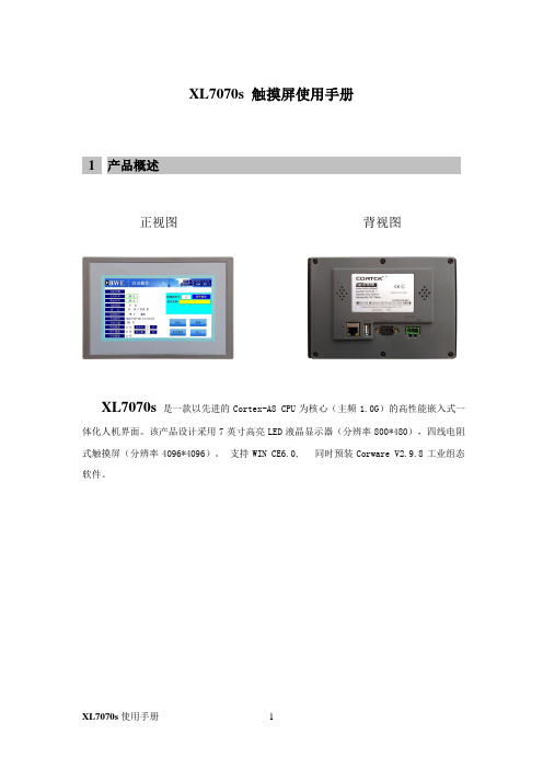
XL7070s 触摸屏使用手册1 产品概述正视图背视图XL7070s是一款以先进的Cortex-A8 CPU为核心(主频1.0G)的高性能嵌入式一体化人机界面。
该产品设计采用7英寸高亮LED液晶显示器(分辨率800*480),四线电阻式触摸屏(分辨率4096*4096)。
支持WIN CE6.0, 同时预装Corware V2.9.8工业组态软件。
·液晶屏: 7寸TFT液晶屏、LED背光、颜色65535·分辨率:800*480·显示亮度:350cd/m2· C P U:ARM Cortex A8,主频1.0G·内存:256M DDRII RAM·触摸屏:四线电阻式,点动100万次以上·存储设备:256M NAND FLASH·SD卡扩展:可选,最大可扩展32G·接口:1*RS232、1*RS485、1*USB 2.0、1*LAN ·实时时钟:有·蜂鸣器:有·重量: 1.04 Kg·防护等级: IP 65(前面板)·耐压测试: 500V AC 1分钟·抗干扰性:工频磁场干扰度5级,磁场强度100A/m 2 外观尺寸开孔图3 挂钩安装说明1.将TPC放置于安装槽内2.将挂钩勾脚放于TPC侧面安装孔内,用十字起拧紧螺丝,安装完成。
4 电源连接接线步骤:步骤1:将DC24V电源线剥线后插入电源插头接线端子中;步骤2:使用一字螺丝刀将电源插头螺丝锁紧;步骤3:将电源插头插入产品的电源插座。
电源插头示意图及引脚定义如下:5 外部接口5.1 接口说明LAN USB COM1/2 电源5.2 串口引脚定义5.3 TPC与PLC的连接TPC Siemens S7-200系列PPI 9针D形母头9针D形公头TPC Omron C/CV/CS/CJ/CP系列HostLink 9针D形母头9针D形公头PORT口接口PIN引脚定义COM COM12 RS232 RXD3 RS232 TXD5 GNDCOM27 RS485 +8 RS485 -7 RS485 +8 RS485 - 8 D -3 D +2 RX 2 TX2-5k 电阻,推荐3.3K 2-5k 电阻,推荐3.3KTPC 三菱电机FX 系列编程口 9针 D 形母头 8针 Din 圆形公头6 工程下载6.1 工程下载方法一:6.1.1 硬件连接连接方式:网线连接6.1.2 启动TPC使用24V 直流电源给TPC 供电,开机启动后屏幕出现“CORTEK ”logo ,此时不需要任何操作,系统将自动进入工程运行界面。


CUSTOMER APPROVAL SHEETCompany NameMODELA070FW03 VDCUSTOMERAPPROVEDTitle : Name :□ APPROVAL FOR SPECIFICATIONS ONLY (Spec. Ver. )□ APPROVAL FOR SPECIFICATIONS AND ES SAMPLE (Spec. Ver. ) □ APPROVAL FOR SPECIFICATIONS AND CS SAMPLE (Spec. Ver. ) □CUSTOMER REMARK :AUO PM : Orion PengP/N : 97.07A04.D00Comment :1 Li-Hsin Rd. 2. Science-Based Industrial ParkHsinchu 300, Taiwan, R.O.C.Tel: +886-3-500-8899 Fax: +886-3-577-2730Doc. version : 0.0 Total pages : 28A UOCo n fi de n ti a lF or Pr om a t eI nt er na l Us eOn l y / 2010/1/5Product Specification7.0" COLOR TFT-LCD MODULEModel Name :A070FW03 VDPlanned Lifetime: From 2009/Dec To2011/DecPhase-out Control:From 2011/Jul To 2011/DecEOL Schedule:2011/Jul< >Preliminary Specification < >Final SpecificationNote: The content of this specification is subject to change.© 2009 AU Optronics All Rights Reserved, Do Not Copy.A UOCo n fi de n ti a lF or Pr om a t eI nt er na l Us eOn l y / 2010/1/5Page:1/28Record of RevisionVersion Revise Date Page Content0.0 2009/03/10All First DraftA UOCo n fi de n ti a lF or Pr om a t eI nt er na l Us eOn l y / 2010/1/5Page:2/28ContentsA. General Information.....................................................................................................................................3B.Outline Dimension (4)1. TFT-LCD Module – Front View....................................................................................................................42. TFT-LCD Module – Rear View....................................................................................................................5 C.Electrical Specifications .............................................................................................................................6 1. TFT LCD Panel Pin Assignment .................................................................................................................6 2. Backlight Pin Assignment............................................................................................................................7 3. Absolute Maximum Ratings.........................................................................................................................7 3. Electrical DC Characteristics.......................................................................................................................8 4. Electrical AC Characteristics.....................................................................................................................10 6. Power On/Off Characteristics....................................................................................................................17 D. Optical Specification .................................................................................................................................18 E. Reliability Test Items .................................................................................................................................21 F.Packing and Marking.................................................................................................................................24 1. Packing Form............................................................................................................................................24 2. Module/Panel Label Information ...............................................................................................................25 3. Carton Label Information...........................................................................................................................25 G.Precautions (26)A UOCo n fi de n ti a lF or Pr om a t eI nt er na l Us eOn l y / 2010/1/5Page:3/28A. General InformationThis product is for portable DVD and digital photo frame application. NO. ItemUnit Specification Remark1 Screen Sizeinch 7.0(Diagonal)2 Display Resolution dot480RGB(W)×234(H)3 Overall Dimensionmm 164.9 (W)×100(H)×5.7(D) Note 1 4 Active Area mm154.08(W)×86.58(H) 5 Pixel Pitchmm 0.107(W)×0.370(H)6 Color Configuration --R. G. B. Stripe Note 2 7 NTSC Ratio% 48%8 Display Mode -- Normally White 9Panel surface Treatment -- Anti-Glare, 3H10 Weight g TBD 11 LCD Module Power ConsumptionW 2.212 Viewing direction6 o’clock (gray inversion)Note 1: Not include blacklight cable and FPC. Refer next page to get further information. Note 2: Below figure shows dot stripe arrangement.( 1………………………..234)A UOCo n fi de n ti a lF or Pr om aPage:4/28ALL RIGHTS STRICTLY RESERVED. ANY PORTION OF THIS PAPER SHALL NOT BE REPRODUCED, COPIED, OR TRANSFORMED TO ANY OTHER FORMSWITHOUT PERMISSION FROM AU OPTRONICS CORP.B. Outline Dimension (D00)1. TFT-LCD Module – Front ViewA UOPage:5/28ALL RIGHTS STRICTLY RESERVED. ANY PORTION OF THIS PAPER SHALL NOT BE REPRODUCED, COPIED, OR TRANSFORMED TO ANY OTHER FORMSWITHOUT PERMISSION FROM AU OPTRONICS CORP.2. TFT-LCD Module – Rear ViewA UPage:6/28C. Electrical Specifications1. TFT LCD Panel Pin AssignmentPin no Symbol I/O DescriptionRemark1 GND - Ground for logic circuit2 V CC I Supply voltage of logic control circuit for scan driver3 V GL I Negative power for scan driver4 V GH IPositive power for scan driver5 STVR I/O Vertical start pulse Note 16 STVL I/O Vertical start pulse Note 17 CKV I Shift clock input for scan driver 8 U/D I UP/DOWN scan control input Note 1,29 OEV I Output enable input for scan driver 10 VCOM I Common electrode driving signal 11 VCOM I Common electrode driving signal12 L/R I LEFT/RIGHT scan control input Note 1,213 MOD I Sequential sampling and simultaneous sampling setting14 OEH IOutput enable input for data driver15 STHL I/O Start pulse for horizontal scan lineNote 1 16 STHR I/O Start pulse for horizontal scan lineNote 1 17 CPH3 I Sampling and shifting clock pulse for data driver18 CPH2 I Sampling and shifting clock pulse for data driver19 CPH1 I Sampling and shifting clock pulse for data driver20 V CC I Supply voltage of logic control circuit for data driver21 GND - Ground for logic circuit22 VRIAlternated video signal input(Red) 23 VGI Alternated video signal input(Green) 24VBI Alternated video signal input(Blue)25 AV DD I Supply voltage for analog circuit 26AV SS-Ground for analog circuitA UOCo n fi de n ti a lF or Pr om a t eI nt er na l Us eOn l y / 2010/1/5Page:7/28I: Input pin; P: Power pin; G: Ground pin; C: capacitor pinRefer to figure as below:Pin26 Pin12. Backlight Pin AssignmentRecommended connector : E&T H201K-P020N-02BPin no Symbol I/O Description Remark1 VLEDPLED power supply2GNDLEDP LED ground3. Absolute Maximum RatingsItemSymbol Condition Min. Max. Unit RemarkV CCGND=0-0.3 7 V AV DD AGND=0-0.3 7VV GH -0.3 18 V V GL GND=0-15 0.3 V Power voltageV GH -V GL-33VV i-0.3 AV DD +0.3 VNote 3 V I-0.3 V CC +0.3 V Note 4 Input signal voltageVCOM-2.9 7.5 VNote 1: Functional operation should be restricted under ambient temperature (25℃).Note 2: Maximum ratings are those values beyond which damages to the device may occur. Functionaloperation should be restricted to the limits in the Electrical Characteristics chapter.Note 3: VR, VG, VB.Note 4: STHL, STHR, OEH, LRC, CPH1~CPH3, STVD, STVU, OEV, CKV, UDC, MODA UOCo n fi de n ti a lF or Pr om a t eI nt er na l Us eOn l y / 2010/1/5Page:8/283. Electrical DC Characteristicsa. Typical Operation Condition (AGND =GND = 0V)ItemSymbol Min. Typ. Max. Unit Remark V CC3 3.3 5.5 VDigital powerAV DD4.5 55.5 V Analog PowerV GH 14.3 15 15.7 V Positive power supply for gate driver Power VoltageVGL-10.5 -10 -9.5 V Negative power supply for gate driverV iA 0.4 - AV DD -0.4V Refer to Horizontal timing V iAC - 4- V AC component Video signal amplitude(VR,VG,VB) V iDC -AV DD /2 -VDC componentH LevelVIH 0.8xVCC - VCC VInputSignal Voltage L Level VIL GND - 0.2xVC VNote 1. V CAC 3.5 5.6 6.5 VAC component Gamma referencevoltageV CDC1.41.72.0VDC component Note 1: STHL, STHR, OEH, LRC, CPH1~CPH3, STVD, STVU, OEV, CKV, UDC, MOD.Note2: Must follow power On/Off Sequence.Note 3: If input signal amplitude is 3.3V, recommend value for Vcc is 3.3VIf input signal amplitude is 5V, recommend value for Vcc is 5Vb. Current Consumption (AGND=GND=0V)ParameterSymbol ConditionMin. Typ. Max. Unit RemarkInput current for V GH I GH V GH =15V- 0.12 1.0 m A Input current for V Gl I GL V Gl =-10V- 0.15 1.0 mA Input current for Vcc I CC DV CC =3.3- 2 6.0 mA Input current for Avdd I DDAV DD =5V-5.330mAA UOCo n fi de n ti a lF or Pr om a t eI nt er na l Us eOn l y / 2010/1/5Page:9/28c. Backlight Driving ConditionsThe backlight (LED module, Note 1) is suggested to drive by constant current with typical value.ParameterSymbol Min. Typ. Max. Unit Remark LED light bar CurrentI L-- 200 -- mABL Power ConsumptionP BL --2.1 --WNote 1 LED Life TimeL L 10,000 ---- Hr Note 2, 3Note 1: The LED driving condition is defined for LED module (24 LED). The voltage range will be 8.7 to 11.6V based on suggested driving current set as 200mA .Note 2: Define “LED Lifetime”: brightness is decreased to 50% of the initial value. LED Lifetime isrestricted under normal condition, ambient temperature = 25℃ and LED lightbar current =200mA .Note 3: If it uses larger LED lightbar voltage more than 200mA , it maybe decreases the LED lifetime.A UOCo n fi de n ti a lF or Pr om a t eI nt er na l Us eOn l y / 2Page:10/284. Electrical AC Characteristicsa. Signal AC CharacteristicsParameterSymbol Min. Typ. Max. Unit. Remark Clock cycle time t CPH100 103 107 ns CPH1 CPH pulse duty t CWH 405060%CPH1CPH pulse delay t C12 30 t CPH /3 t CPH /2 ns CPH1STH setup time t SUH 20 - - ns STHR,STHL STH hold time t HDH 20- - ns STHR,STHL STH pulse width t STH 1 t CPH STHR,STHL STH period t H 61.8 63.7 66.1 μs STHR,STHL OEH pulse width t OEH 1 - - t CPH OEH (Note 1)Sample and hold disable timet DIS1 1 - - t CPH Note 2 OEV pulse width t OEV 2.0 3.4 6.5 μs OEV CKV pulse width t CKV 1.0 3.1 4.68 μs CKV Clean enable timet DIS2 1.0- 1 t OEVμs Note 3 Horizontal display start t SH 1t CPH Horizontal display timing ranget DH 480t CPH STV setup time t SUV 400 -- ns STVU, STVD STV hold time t HDV 400 -- ns STVU, STVD STV pulse width t STV - -1t H STVU, STVDVertical display start t SV 3t H Vertical display timing ranget DV 234 t HVCOM rising time t rCOM - 5 μs VCOM falling time t fCOM- 5 μs VCOM delay time t DCOM 2 - - μs TFT charging time t ch 55 - - μs Output time delay t del 3 - - μs Setup time of analog VR/VG/VBt asu 60 - - ns Hold time of analog VR/VG/VBt ahd 40 - - ns Frame rate5060-HzNote 1: The maximum pulse width of OEH should refer to the minimum of tDIS1 and the hsyncback porch.Note 2: t DIS1 is time difference between OEH and STHL.Note 3: t DIS2 is time difference between OEV and CKVA UOCo n fi de n ti a lF or Pr om a t eI nt er na l Us eOn l y / 2010/1/5Sampling clock timingVersion:0.0Page: 15/28ALL RIGHTS STRICTLY RESERVED. ANY PORTION OF THIS PAPER SHALL NOT BE REPRODUCED, COPIED, OR TRANSFORMED TO ANY OTHER FORMS WITHOUT PERMISSION FROM AU OPTRONICS CORP.Vertical timing (From up to down)a lUs e On ly / 2010/1/5Version:0.0Page: 16/28ALL RIGHTS STRICTLY RESERVED. ANY PORTION OF THIS PAPER SHALL NOT BE REPRODUCED, COPIED, OR TRANSFORMED TO ANY OTHER FORMS WITHOUT PERMISSION FROM AU OPTRONICS CORP.Page: 17/28 6. Power On/Off CharacteristicsPower OnPage:18/28D. Optical SpecificationAll optical specification is measured under typical condition (Note 1, 2)Item Symbol Condition Min. Typ. Max. Unit Remark Response TimeRise FallTr Tfθ=0°-- --12 1824 36ms ms Note 3 Contrast ratioCRAt optimizedviewing angle 300 400 -- Note 4TopBottom LeftViewing AngleRight 30 50 50 5040 65 65 65 -- -- -- -- deg. Note 5Brightness Y Lθ=0° 320 400 -- cd/m 2 Note 6 X θ=0° 0.25 0.30 0.35 ChromaticityWhiteY θ=0° 0.27 0.32 0.37 UniformityΔY L%7075 -- %Note 7Note 1: Ambient temperature =25℃, and LED lightbar current I L = 200 mA . To be measured in the dark room.Note 2: To be measured on the center area of panel with a viewing cone of 1° by Topcon luminance meterBM-5A, after 15 minutes operation.Note 3: Definition of response time:The output signals of photo detector are measured when the input signals are changed from“black” to “white”(falling time) and from “white” to “black”(rising time), respectively.The response time is defined as the time interval between the 10% and 90% of amplitudes.Refer to figure as below.A UOCo n fi de n ti a lF or Pr om 1/5Note 4.Definition of contrast ratio:Contrast ratio is calculated with the following formula.statusBlack"" at is LCD when output detector Photo statusWhite"" at is LCD when output detector Photo (CR) ratio Contrast =Note 5. Definition of viewing angle, θ, Refer to figure as below.Note 6. Measured at the center area of the panel when all the input terminals of LCD panel areelectrically opened.Note 7: Luminance Uniformity of these 9 points is defined as below:A UOCo n fi de n ti a lF or Pr om a t eI nt er nA UOCo n fi de n ti a lF or Pr om a t eI nt er na l Us eOn l y / 2010/1/5Page:21/28E. Reliability Test ItemsNo. Test itemsConditions Remark1 High Temperature Storage240Hrs2 Low Temperature Storage Ta= -2240Hrs3 High Ttemperature Operation Tp240Hrs4 Low Temperature Operation Ta= -1 240Hrs5 High Temperature & High HumidityTp= 580% RH 240Hrs Operation6 Heat Shock -20d/1hr~70d/1hr judge 50cyclesNon-operation7 Electrostatic DischargeContact = ± 4 kV, class B Air = ± 8 kV, class BNote 4 8Image Sticking25, 4hrsNote 5Frequency range : 10~55HzStoke: 1.5mmSweep: 10 Hz ~55 Hz 2 hours for each direction of X,Y,Z9Vibration4 hours for Y directionNon-operationJIS C7021, A-10condition A : 15 minutes10 Mechanical Shock100G . 6ms, ±X,±Y,±Z3 times for each directionNon-operation JIS C7021,A-7condition C 11 Vibration (With Carton)Random vibration:0.015G 2/Hz from 5~200Hz–6dB/Octave from 200~500Hz IEC 68-3412 Drop (With Carton)Height: 60cm1 corner, 3 edges, 6 surfaces13 Pressure5kg, 5sec Note 6Note 1: Ta: Ambient Temperature. Tp: Panel Surface TemperatureNote 2: In the standard conditions, there is not display function NG issue occurred. All the cosmeticspecification is judged before the reliability stress.Note 3: All the cosmetic specification is judged before the reliability stress.Note 4 : All test techniques follow IEC6100-4-2 standard.A UOCo n fi de n ti a lF or Pr om a t eI nt er na l Us eOn l y / 2010/1/5Page:22/28Contact Discharge :330Ω, 150pF, 1sec, 8 point, 25times/pointgray pattern. After 20 minutes, the mura is less than JND 2.5Note 6: The panel is tested as figure. The jig is ψ10 mm made by Cu with rubber and the loadingspeed is 3mm/min on position 1~5. After the condition, no glass crack will be found and panelfunction check is OK.( no guarantee LC mura 、LC bubble)A UOCo n fi de n ti a lF or Pr om a t eI nt eUs eOn l y / 201Page:23/28A UOCo n fi de n ti a lF or Pr om a t eI nt er na l Us eOn l y / 2010/1/5Page:24/28F. Packing and Marking1. Packing FormA UOCo n fi de n ti a lF or Pn l y2. Module/Panel Label InformationThe module/panel (collectively called as the “Product”) will be attached with a label of Shipping Numberwhich represents the identification of the Product at a specific location. Refer to the Product outline drawing for detailed location and size of the label. The label is composed of a 22-digit serial number and printed with code128 with the following definition:Example:501M06ZL06123456781Z05: Product Manufacturing Week Code: WK50 Product Version: Version 1 Product Manufactuing Factory: M063. Carton Label InformationThe packing carton will be attached with a carton label where packing Q’ty, AUO Model Name, AUO PartNumber, Customer Part Number (Optional) and a series of Carton Number in 13 or 14 digits are printed. TheCarton Number is apparing in the following format:Refer to the drawing of packing format for the location and size of the carton label.A UOCo n fi de n ti a lF or Pr om a t eI nt er na l Us eOn l y / 2010/1/5G. Precautions1. Do not twist or bend the module and prevent the unsuitable external force for display module during assembly.2. Adopt measures for good heat radiation. Be sure to use the module with in the specified temperature.3. Avoid dust or oil mist during assembly.4. Follow the correct power sequence while operating. Do not apply the invalid signal, otherwise, it will cause improper shut down and damage the module.5. Less EMI: it will be more safety and less noise.6. Please operate module in suitable temperature. The response time & brightness will drift by different temperature.7. Avoid to display the fixed pattern (exclude the white pattern) in a long period, otherwise, it will cause image sticking.8. Be sure to turn off the power when connecting or disconnecting the circuit. 9. Polarizer scratches easily, please handle it carefully. 10. Display surface never likes dirt or stains.11. A dewdrop may lead to destruction. Please wipe off any moisture before using module.12. Sudden temperature changes cause condensation, and it will cause polarizer damaged.13. High temperature and humidity may degrade performance. Please do not expose the module to the direct sunlight and so on.14. Acetic acid or chlorine compounds are not friends with TFT display module.15. Static electricity will damage the module, please do not touch the module without any groundeddevice.16. Do not disassemble and reassemble the module by self.17. Be careful do not touch the rear side directly.18. No strong vibration or shock. It will cause module broken.19. Storage the modules in suitable environment with regular packing.20. Be careful of injury from a broken display module.21. Please avoid the pressure adding to the surface (front or rear side) of modules, because it will causethe display non-uniformity or other function issue.A UOCo n fi de n ti a lF or Pr om a t eI nt er na l Us eOn l y / 2010/1/5。
Document No. DC140-000581 Revision 1.4TO : SolomonDate : Mar, 20, 2009HannStar Product Specification(Formal)7” Color TFT-LCD ModuleModel: HSD070IDW1-D**Note: 1.Please contact HannStar Display Corp. before designing your product based on this module specification.2.The information contained herein is presented merely to indicate the characteristics andperformance of our products. No responsibility is assumed by HannStar for any intellectualproperty claims or other problems that may result from application based on the moduledescribed herein.3.The mark “ ** ” of Model means sub-model code.Document No. DC140-000581 Revision 1.4Record of RevisionsRev. Date Sub-Model Description of changeFormal Product Specification was first issued.1.4 Feb, 25, 2009 -----Document No. DC140-000581 Revision 1.4Contents1.0 General description ……………………………….… p.42.0 Absolute maximum ratings …………………………. p.53.0 Optical characteristics ………………………………. p.64.0 Block diagram ……………………………..……….. p.105.0 Interface pin connection ……………………………. p.116.0 Electrical characteristics ……………………………. p.137.0 Reliability test items…………………………………… p.218.0 Outline dimension …………………………….…… p.229.0 Lot mark ……………………………………………... p.2410.0 Package specification ………………………………. p.2511.0 General precaution ……………………………………. p.26Document No. DC140-000581Revision1.41.0 GENERAL DESCRIPTION1.1 IntroductionHannStar Display model HSD070IDW1-D is a color active matrix thin film transistor (TFT) liquid crystal display (LCD) that uses amorphous silicon TFT as a switching device. This model is composed of a TFT LCD panel, a driving circuit and a back- light system. This TFT LCD has a 7.0 (16:9) inch diagonally measured active display area with WVGA (800 horizontal by 480 vertical pixel) resolution. 1.2 Features■ 7 (16:9 diagonal) inch configuration■ 6 bits + FRC driver with 1channel TTL interface ■ LED Backlight■ Up/Down, Left/Right reversion selection ■ RoHS/ Halogen Free Compliance 1.3 Applications■ Automotive ■ Mobile NB■ Digital Photo frame■ Multimedia applications and Others AV system 1.4 General informationItem Specification UnitOutline Dimension 164.9 x 100.0 x 5.7 (Typ.) mm Display area 153.6(H) x 86.64(V) mm Number of Pixel 800 RGB(H) x 480(V) pixels Pixel pitch 0.192(H) x 0.1805(V) mm Pixel arrangement RGB Vertical stripe Display mode Normally whiteSurface treatment Antiglare, Hard-Coating(3H) with EWV film Weight 170 (Typ.)g Back-light Single LED (Side-Light type) PowerConsumptionB/L System1.68(Max.)W1.5 Mechanical InformationItemMin. Typ. Max. Unit Horizontal(H)164.6 164.9 165.2 mm Vertical(V)99.7 100.0 100.3 mm ModuleSizeDepth(D)5.4 5.76.0 mm Weight (Without inverter)-170-gDocument No. DC140-000581 Revision 1.4 2.0 ABSOLUTE MAXIMUM RATINGS2.1 Electrical Absolute Rating2.1.1 TFT LCD ModuleItem Symbol Min. Max. Unit NoteVcc -0.3 6.0 V GND=0V GH0.3 40 V GND=0 Power supply voltageV GL-20 0.3 V GND=0AV DD0.5 15 V AGND=0V COM0 6 VLogic Signal Input Level V I-0.3 Vcc +0.3 V2.1.2 Back-Light UnitItem Symbol Typ. Max. Unit Note LED current I L140 -mA (1) (2)(3)LED voltage V L10.5 -V (1) (2)(3)Note(1) Permanent damage may occur to the LCD module if beyond this specification.Functional operation should be restricted to the conditions described undernormal operating conditions.(2) Ta =25±2℃(3) Test Condition: LED current 140 mA. The LED lifetime could be decreased ifoperating IL is larger than 140mA.2.2 Environment Absolute RatingItem Symbol Min. Max. Unit Note Operating Temperature T opa-20 70 ℃Storage Temperature T stg-30 80 ℃Document No. DC140-000581 Revision 1.4 3.0 OPTICAL CHARACTERISTICS3.1 Optical specificationItem Symbol Condition Min. Typ. Max. Unit Note Contrast CR 400 500 -(1)(2) Rising T R- 5 7Responsetime Falling TF -20 28msec (1)(3)White luminance (Center) Y L280 350 -cd/m2(1)(4)(I L=140mA) W x0.260 0.310 0.360Colorchromaticity (CIE1931) WhiteW yΘ=0Normalviewingangle0.280 0.330 0.380ΘL60 75 -Hor.ΘR60 75 -ΘU40 60 -ViewingangleVer.ΘD CR>1050 70 -(1)(4)Brightness uniformity B UNIΘ=0 70 - -% (5)(7) Optima View Direction 6 O’clock(6)3.2 Measuring Condition■Measuring surrounding: dark room■LED current I L: 140mA■Ambient temperature: 25±2o C■15min. warm-up time.3.3 Measuring Equipment■FPM520 of Westar Display technologies, INC., which utilized SR-3 for Chromaticityand BM-5A for other optical characteristics.■Measuring spot size: 20 ~ 21 mmDocument No. DC140-000581 Revision 1.4Document No. DC140-000581 Revision 1.4Document No. DC140-000581 Revision 1.4Document No. DC140-000581Revision1.44.0 BLOCK DIAGRAM4.1 TFT LCD Module4.2 Pixel FormatDocument No. DC140-000581 Revision 1.4 5.0 INTERFACE PIN CONNECTION5.1 TFT LCD ModuleCN2 (Input signal): FPC Down Connector, (FH28-60S-0.5SH (HIROSE), 60pin,pitch = 0.5mm) Terminalno.Symbol I/O Function1 AGND P Analog Ground2 AVDD P Analog Power3 VCC P Digital Power4 R0 I Data Input(LSB)5 R1 I Data Input6 R2 I Data Input7 R3 I Data Input8 R4 I Data Input9 R5 I Data Input10 R6 I Data Input11 R7 I Data Input(MSB)12 G0 I Data Input(LSB)13 G1 I Data Input14 G2 I Data Input15 G3 I Data Input16 G4 I Data Input17 G5 I Data Input18 G6 I Data Input19 G7 I Data Input(MSB)20 B0 I Data Input(LSB)21 B1 I Data Input22 B2 I Data Input23 B3 I Data Input24 B4 I Data Input25 B5 I Data Input26 B6 I Data Input27 B7 I Data Input(MSB)28 DCLK I Clock input29 DE I Data Enable signal30 HSD I Horizontal sync input.Negative polarity31 VSD I Vertical sync input.Negative polarity32 MODE3 I DE/SYNC mode select .normally pull high H:DE mode.L:HSD/VSD mode33 RSTB Iglobal reset pin.Active low to enter reset state.suggest to connecting with an RC reset circuit for stability .normally pullhigh.34 STBYB Istandby mode,normally pull high STBYB="1",normal operation STBYB="0",timming control ,soruce driver will turn off,all output are high-Z35 SHLR I Source right or left sequence control.SHLR="L",shift left:last data=S1<-S2…S1200=first data SHLR="H",shift right:first data=S1->SS2…S1200=last dataDocument No. DC140-000581 Revision 1.4 Terminalno.Symbol I/O Function36 VCC P Digital Power37 UPDN I gate up or down scan control. UPDN="L" , DOWN shift : G1->G2…->G480 ; UPDN="H", up shift: G1<-G2…<-G48038 GND P Digital Ground39 AGND P Analog Ground40 AVDD P Analog Power41 VCOMin I For external VCOM DC input(Optional)42 DITH I Dithering setting: DITH="H" 6bit resolution (last 2 bits of input data truncated) (default setting) DITH="L" 8bitresolution43 NC - Not connect44 NC - Not connect45 V10 P Gamma correction voltage reference46 V9 P Gamma correction voltage reference47 V8 P Gamma correction voltage reference48 V7 P Gamma correction voltage reference49 V6 P Gamma correction voltage reference50 V5 P Gamma correction voltage reference51 V4 P Gamma correction voltage reference52 V3 P Gamma correction voltage reference53 V2 P Gamma correction voltage reference54 V1 P Gamma correction voltage reference55 NC - Not connect56 VGH P Positive Power for TFT57 VCC P Digital Power58 VGL P Negative Power for TFT59 GND P Digital Ground60 NC - Not connect5.2 Back-Light UnitCN1 LED Power Source (BHSR-02VS-1) or equivalentMating Connector: (SBHT-002T-P0.5) or equivalentTerminal no. Symbol Function1 VL LED power supply (high voltage)2 GL LED power supply (low voltage)Document No. DC140-000581Revision1.46.0 ELECTRICAL CHARACTERISTICS6.1 TFT LCD ModuleItem SymbolMin.Typ.Max.UnitNoteVcc2.73.0 3.5 V V GH 14.5 15 20 V V GL -10 -7 -6.5 V Supply VoltageAV DD9.85 10 10.15 V VCOM V COMin - 3.9 - V V iH 0.7 Vcc- Vcc V Note (1)Input signal voltageV iL 0 - 0.3 VccV I DD- 5.426 - mA Vcc =3.0V I ADD - 24.1 - mA AV DD =10 V (Black)I GH - 0.128 - mA V GH =15V Current of powersupplyI GL- 0.344 - mA V GL = -7VInput level ofV1~V5 Vx AVDD/2- AVDD-0.1-V Input level ofV6~V10Vx0.1-AVDD/2-VNote (1): HSYNC, VSYNC, DE, Digital DataNote (2): Be sure to apply the power voltage as the power sequence spec. Note (3): DGND=AGND=0V,)Document No. DC140-000581 Revision 1.4Document No. DC140-000581 Revision 1.4 Note (3) Suggested Schematic of LED Back-Light DriverSuggested Schematic of LED Back-Light DriverDocument No. DC140-000581 Revision 1.46.3 AC CharacteristicsItem Symbol Min. Typ. Max. Unit Note DCLK cycle time Tcph 25 nsDCLK frequency fclk 30 40 MHzDCLK pulse duty Tcwh 40 50 60 %VSD setup time Tvst 8 nsVSD hold time Tvhd 8 nsHSD setup time Thst 8 nsHSD hold time Thhd 8 nsData setup time Tdsu 8 nsData hold time Tdhd 8 nsDE setup time Tesu 8 nsDE hold time Tehd 8 nsHorizontal display area thd 800 TcphHSD period time th 928 TcphHSD pulse width thpw 1 48 TcphHSD back porch thb 40 TcphHSD front porch thfp 40 TcphVertical display area tvd 480 thVSD period time tv 525 thVSD pulse width tvpw 3 thVSD back porch tvb 29 thVSD front porch tvfp 13 thDocument No. DC140-000581 Revision 1.4Document No. DC140-000581 Revision 1.4Document No. DC140-000581 Revision 1.4Item Min. Typ. Max. UnitT0 0.5 -- 20 msecT1 16 msecT2 20 msecT3 10 msecDocument No. DC140-000581 Revision 1.46.6 Gamma circuit** Suggested Gamma Circuit. **Document No. DC140-000581 Revision 1.47.0 Reliability test itemsNo.Item Conditions Remark1 High Temperature Storage Ta=+80o C, 240hrs2 Low Temperature Storage Ta=-30o C, 240hrs3 High Temperature Operation Ta=+70o C, 240hrs4 Low Temperature Operation Ta=-20o C, 240hrs5 High Temperature and High Humidity(operation)Ta=+60o C, 90%RH, 240hrs6 Thermal Cycling Test (non operation) -30o C(30min) → +80o C(30min), 200cycles7 Electrostatic Discharge ±200V,200pF(0Ω) 1 time/each terminal8 Vibration 1.Random:1.04Grms, 5~500Hz, X/Y/Z,30min/each direction2. Sine:Freq. Range: 8~33.3HzStoke: 1.3mmSweep: 2.9G, 33.3~400HzX/Z: 2hr, Y: 4hr, cyc: 15min9 Shock 100G, 6ms, ±X, ±Y, ±Z3 time for each direction JIS C7021, A-10 (Condition A)10 Vibration (with carton) Random: 0.015G^2/Hz, 5~200Hz-6dB/Octave, 200~400HzXYZ each direction: 2hr11 Drop (with carton) Height: 60cm1 corner, 3 edges, 6 surfacesJIS Z0202Note: There is no display function NG issue occurred, all the cosmetic specification is judged before the reliability stress.Document No. DC140-000581 Revision1.48.0 OUTLINE DIMENSION8.1 Outline DimensionU Unit : mmDocument No. DC140-000581 Revision 1.4BM Assembly Tolerance0 ≦(A’-A) ≦2 (mm)│B’-B│≦1 (mm)Document No. DC140-000581 Revision 1.4Document No. DC140-000581 Revision 1.4 10.0 PACKAGE SPECIFICATION10.1 Packing form(1) Package quantity in one carton: 80 pieces.(2) Carton size: 451mm×375mm×284mm.10.2 Packing assembly drawingsMaterial NoticeBox Corrugated Paper Board (AB Flute) Partition/Pad Corrugated Paper Board (B Flute)Corner Pad Corrugated Paper Board (AB Flute)ESD bag PEDocument No. DC140-000581 Revision 1.4 11.0 GENERAL PRECAUTION11.1 Use RestrictionThis product is not authorized for use in life supporting systems, aircraft navigation control s ystems, military systems and any other application where performance failure could bel ife threatening or otherwise catastrophic.11.2 Disassembling or ModificationD o not disassemble or modify the module. It may damage sensitive parts inside LCDm odule, and may cause scratches or dust on the display. HannStar does not warrant the m odule, if customers disassemble or modify the module.11.3 Breakage of LCD Panel11.3.1.If LCD panel is broken and liquid crystal spills out, do not ingest or inhale liquidcrystal, and do not contact liquid crystal with skin.11.3.2. If liquid crystal contacts mouth or eyes, rinse out with water immediately.11.3.3. If liquid crystal contacts skin or cloths, wash it off immediately with alcohol andrinse thoroughly with water.11.3.4. Handle carefully with chips of glass that may cause injury, when the glass isbroken.11.4 Electric Shock11.4.1. Disconnect power supply before handling LCD module.11.4.2. Do not pull or fold the LED cable.11.4.3. Do not touch the parts inside LCD modules and the fluorescent LED’s connectoror cables in order to prevent electric shock.11.5 Absolute Maximum Ratings and Power Protection Circuit11.5.1. Do not exceed the absolute maximum rating values, such as the supply voltagevariation, input voltage variation, variation in parts’ parameters, environmentaltemperature, etc., otherwise LCD module may be damaged.11.5.2. Please do not leave LCD module in the environment of high humidity and hightemperature for a long time.11.5.3. It’s recommended to employ protection circuit for power supply.Document No. DC140-000581 Revision 1.411.6 Operation11.6.1 Do not touch, push or rub the polarizer with anything harder than HB pencil lead.11.6.2 Use fingerstalls of soft gloves in order to keep clean display quality, when personshandle the LCD module for incoming inspection or assembly.11.6.3 When the surface is dusty, please wipe gently with absorbent cotton or other softmaterial.11.6.4 Wipe off saliva or water drops as soon as possible. If saliva or water drops contactwith polarizer for a long time, they may causes deformation or color fading.11.6.5 When cleaning the adhesives, please use absorbent cotton wetted with a littlepetroleum benzine or other adequate solvent.11.7 MechanismPlease mount LCD module by using mouting holes arranged in four corners tightly.11.8 Static Electricity11.8.1 Protection film must remove very slowly from the surface of LCD module top revent from electrostatic occurrence.11.8.2. Because LCD module use CMOS-IC on circuit board and TFT-LCD panel, it is veryw eak to electrostatic discharge. Please be careful with electrostatic discharge.P ersons who handle the module should be grounded through adequate methods.11.9 Strong Light ExposureThe module shall not be exposed under strong light such as direct sunlight. Otherwise,display characteristics may be changed.11.10 DisposalWhen disposing LCD module, obey the local environmental regulations.。