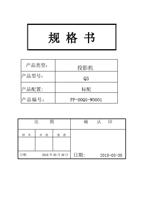
10寸显示屏规格书
- 格式:pdf
- 大小:12.64 MB
- 文档页数:24
一产品外观尺寸198x153x68.5mm二产品接口①②③④⑤⑥⑦Q5标配版①音频输出耳机座端口,连接外部音频信号放大设备或耳机。
②视频、音频信号输入端口,连接VCD、DVD视频信号输出端。
③ TF Card接口,插入U盘可以播放U盘里的音频、视频、图片文件。
④ HDMI高清视频信号端口,连接计算机、DVD的HDMI输出信号端。
⑤ USB接口,插入U盘可以播放U盘里的音频、视频、图片文件⑥计算机信号输入端口,连接计算机的输出信号端。
三:产品简介Q5投影机采用LED光源,具有低功耗、反应速度快、逼真的色彩还原处理色彩艳丽清晰、寿命长(三万小时超长寿命)、对比度高(达1000:1)、分辨率80 0*480封闭式的防尘及散热设计,工作噪音低;支持外置TF 卡(最大32G)及机器内存储的OFFICE 文件直接读取并投影,支持机器内存或TF 卡播放高清视频,图片等多媒体文件,全解码480p, 720P. 1080P 等高清片源,可选择简体中文、繁体中文、日语、英语、西班牙语、德语、意大利语、法语、俄语等20 多种国际语言显示。
MHL( Mobile High-Definition Link) 移动终端高清影音标准接口,是一种连接便携式消费电子装置的影音标准接口,MHL仅使用一条信号电缆,通过标准HDMI输入接口即可呈现于投影机屏幕上, 具有超低的工作电流和待机功耗,可节省电池寿命, 通过一条电缆,就可支持高达 1080p 分辨率的高质量数字高清晰视频,与今天大多数数字电视采用的 HDMI 输入接口兼容,包括了集成的 CEC 功能和逻辑控制。
支持大容量的移动硬盘(500G-2T,移动硬盘需外部供电)四.产品规格:设计标准按GB/T 28037-2011 信息技术投影机通用规范1.产品规格:制定审核批准。
Product SpecificationsCustomerDescription 3.45” TFT LCD ModuleModel Name SGC035COM—54PINDate 2008/6/13Doc. No.Revision BCustomer ApprovalDateThe above signature represents that the product specifications, testing regulation, and warranty in the specifications are acceptedEngineeringCheck Date Prepared DateDoris2008/6/13CONTENTSNo. ITEM PAGE0 RECORD OF REVISION 31 SUMMARY 42 FEATURES 43 GENERAL SPECIFICATIONS 44 ABSOLUTE MAXIMUM RATINGS 45 ELECTRICAL CHARACTERISTICS 56 DC CHARATERISTICS 67 AC CHARACTERISTICS 6~108 OPTICAL CHARATERISTIC 119 TOUCH PANEL 14~1510 INTERFACE 16~1911 BLOCK DIAGRAM 2012 QUALITY ASSURANCE 2113 OUTLINE DRAWING 2214 PACKAGE INFORMATION 2315 PRECAUTIONS 24~26RECORD OF REVISIONSRevision Date Page DescriptionA 2008/2/12 all New CreationB 2008/6/13 18 LCM PIN Definition1. SUMMARYThis technical specification applies to 3.45“color TFT-LCD panel. The 3.45“ color TFT-LCD panel is designed for GPS, camcorder, digital camera application and other electronic products which require high quality flat panel displays. This module follows RoHS.2. FEATURESHigh Resolution: 230,400 Dots (320 RGB x 240). SGC 035COM—54PIN is atransmissive type color active matrix liquid crystal display (LCD) which uses amorphous thin film transistor (TFT) asswitching devices. This product is composed of a TFT LCD panel, driver ICs, FPC, backlight unit and touch panel.,3. GENERAL SPECIFICATIONSParameter Specifications Unit Screen size 3.45(Diagonal) InchDisplay Format 320 RGB x 240 DotActive area 70.08(H) x 52.56(V) mmDot size 73x 219 umPixel Configuration RGB-Stripe Outline dimension 76.9(W) x 63.9(H) x 3.3(D) mm Display Mode Normally white/Transmissive Surface Treatment Haze 20% Display Garmut NTSC 60% Input Interface Digital 24-bit RGB/SERIALRGB/CCIR656/CCIR601Weight (31) g View Angle direction 6 o’clockOperation -20~70 ℃Temperature RangeStorage -30~80 ℃4. ABSOLUTE MAXIMUM RATINGSItem Symbol Condition Min. Max. Unit Remark Power Voltage DVDD,AVDD GND=0 -0.3 5.0 V Input SignalVoltage V in GND=0 -0.3 VDD+0.3 VNOTE Logic OutputVoltageV OUT GND=0 -0.3 VDD+0.3 V NOTENote: Device is subject to be damaged permanently if stresses beyond those absolute maximum ratings listed above1. Temp. ≤ 60℃, 90% RH MAX.Temp. > 60℃, Absolute humidity shall be less than 90% RH at 60℃2.5. ELECTRICAL CHARACTERISTICS 5.1. Operating conditions:Parameter SymbolRatingMin. Typ. Max.Unit ConditionPower Voltage VCC 3.0 3.3 3.6 V Digital Operation CurrentIcc 8.6 mA Gate On Power VGH 14 15 18 V Gate Off Power VGL -11-10 -8V Vcom High Voltage VcomH 3.7 V Note1 Vcom low VoltageVcomL-1.6VNote1Vcom level max VcomA 6 VNote1. VcomH& VcomL :Adjust the color with gamma data. Vp-p should be higher then4V.(Option 5V)Note: Please power on following the sequence VCC Æ VDD5.2 LED driving conditionsParameter Symbol Min. Typ. Max. Unit Remark LED current- 20 - m A Power Consumption - 400 420 mW LED voltage VBL+ 18.619.8 21 V Note 1 LED Life Time - (50,000)- - HrNote 2,3Note 1 : There are 1 Groups LEDILEDNote 2 : Ta = 25℃Note 3 : Brightess to be decreased to 50% of the initial value深圳宏辉成液晶显示有限公司/6. DC CHARATERISTICSParameter SymbolRatingUnit Condition Min. Typ. Max.Low level input voltage V IL 0-0.3VCCVHight level input voltage V IH0.7VCC-VCC V7. AC CHARATERISTICSDigital Parallal RGB interfaceSignal Item Symbol Min Typ Max UnitFrequency Tosc - 156 - ns Dclk High Time Tch - 78 - nsLow Time Tcl - 78 - nsDataSetup Time Tsu 12 - - nsHold Time Thd 12 - - nsPeriod TH - 408 - Tosc Pulse Width THS 5 30 - ToscHsyncBack-Porch Thb 38 ToscDisplay Period TEP - 320 - ToscHsync-den time THE 36 68 88 TsocFront-Porch Thf - 20 - ToscPeriod Tv - 262 - THPulse Width Tvs 1 3 5 TH Vsync Back-Porch Tvb - 15 - TH Display Period Tvd - 240 - THFront-Porch Tvf 2 4 - TH1. Thp + Thb = 68, the user is make up by yourself.2. Tv = Tvs + Tvb + Tvd + Tvf , the user is make up by yourself.3.When SYNC mode is used,1st data start from 68th Dclk after Hsync fallingDigital Serial RGB interfaceSignal Item Symbol Min Typ Max Unit Frequency Tosc - 52 - ns Dclk High Time Tch - 78 - ns Low Time Tcl - 78 - nsData Setup Time Tsu 12 - - nsHold Time Thd 12 - - nsPeriod TH - 1224 - Tosc Pulse Width THS 5 90 - ToscHsyncBack-Porch Thb 114 ToscDisplay Period TEP - 960 - Tosc Hsync-den time THE 108 204 264Front-Porch Thf - 60 - ToscPeriod Tv - 262 - THPulse Width Tvs 1 3 5 THVsync Back-Porch Tvb - 15 - THDisplay Period Tvd - 240 - THFront-Porch Tvf 2 4 - TH Note: 1. Thp + Thb = 204, the user is make up by yourself.2. Tv = Tvs + Tvb + Tvd + Tvf , the user is make up by yourself.3. When SYNC mode is used,1st data start from 204th Dclk after Hsync fallinCCIR601/656 InterfaceSignalData Setup Time Tsu 12 - - ns Hold Time Thd 12 - - ns深圳宏辉成液晶显示有限公司/[_//f+--------------------H " "'= 1560--------------------+jInvalid Data Inva l i d Da t a018,0"'=DOTCLK In va li d DataIn v a l i d Data]---...t--f------------H018, =1440-------------+jslrL//RR[7:0]In va lid DataIn va l i d Dataf---- t.<sP = HBP[6:0]'4+STH[1:0'1-- *. - ----------- IH0,se = 128--- --- ----.!Figure1 CCIR601 Horizontal Timing深圳宏辉成液晶显示有限公司 /手机 : 133 166 766 58 MSN: lcd.sales@ QQ:1378107648Doc. No.SEL[2:0] = 100- 111, NTSCVSYNC HSYNCRR[7:0]tveP = VBP[6:0]DL1DL2DL3IDL2391DL240I---ODD Field VSYNCEVEN FieldHSYNCRR[7:0]tvsP= VBP[6:0] + 1·IODD FieldI IDL1DL2DL3IDL2391DL240ISEL[2:0] = 100- 111, PAL, PALM=OEVEN VSYNCHSYNCRR[7:0]tvsP= VBP[6:0]DL1DL2DL3IDL2791DL280IODD Field VSYNCEVEN Fi l eHSYNCRR[7:0]tvsP= VBP[6:0] + 1·IODD FieldI IDL1DL2DL3IDL2791DL280ISEL[2:0] = 100 - 111, PAL, PALM=1EVEN VSYNCHSYNCRR[7:0]tveP= VBP[6:0]DL1DL2DL3IDL2871DL288 1ODD Field VSYNCEVEN Fi l eHSYNCI深圳宏辉成液晶显示有限公司 /手机 : 133 166 766 58 MSN: lcd.sales@ QQ:1378107648IRR[7:0]lvsP= VBP[6 0] + 1·IDL1DL2DL3IDL287 1DL288 1Figure1CCIR601 Vertical Timing深圳宏辉成液晶显示有限公司 /手机 : 133 166 766 58 MSN: lcd.sales@ QQ:1378107648Figure2 CCIR656 Horizontal Timing深圳宏辉成液晶显示有限公司 /手机 : 133 166 766 58 MSN: lcd.sales@ QQ:1378107648Figure2 CCIR656 Vertical Timing深圳宏辉成液晶显示有限公司 /手机 : 133 166 766 58 MSN: lcd.sales@ QQ:1378107648Figure 3Digital RGB NTSC mode Vertical Data Format for 262THH cycle = 1224tHBP = 204HDISP = 960t HFP = 60DOTCLKHSYNCPixel DataDumm yD0D1----------D 957 D 958 D 959Dum mya ) Horizontal Data Transaction Tim ing V cycle = 262 Lines t VBP = 18VSYNC VDISP = 240 Lines t VFP = 4HSYNC Line 0 b ) Vertical Data Transaction Tim ing Line 239深圳宏辉成液晶显示有限公司 /手机 : 133 166 766 58 MSN: lcd.sales@ QQ:1378107648Figure 3 Data Transaction Timing in Serial RGB (8 bit) Interface (SYNC Mode)深圳宏辉成液晶显示有限公司 /手机 : 133 166 766 58 MSN: lcd.sales@ QQ:1378107648Figure3 Data Transaction Timing in Serial RGB (8 bit) Interface (DE Mode)深圳宏辉成液晶显示有限公司 /手机 : 133 166 766 58 MSN: lcd.sales@ QQ:1378107648Figure3Data Transaction Timing in Parallel RGB (24 bit) Interface (SYNC Mode)深圳宏辉成液晶显示有限公司 /手机 : 133 166 766 58 MSN: lcd.sales@ QQ:1378107648Figure4 Data Transaction Timing in Parallel RGB (24 bit) Interface (DE Mode)7.1.1 Standby ON/OFF Control LQ35NC211 has a power ON/OFF sequence control function. When STB pin is pulled L,blank data is outputted for 5-frames first, form the falling edge of the following VSYNC signal. The blank data would be gray level 255 for normally white LC.Figure5 Standby ON/OFF Control 7.1.2 Clock and Sync waveforms深圳宏辉成液晶显示有限公司 /手机 : 133 166 766 58 MSN: lcd.sales@ QQ:1378107648Figure6 CLK and IHS timing waveformTV FTC LTH B7.2 Reset Timing ChartThe RESET input must be held at least 1ms after power is stable8. OPTICAL CHARATERISTICTa=25±2℃, ILED=20mA Item Symbol Condition Min. Typ. Max. Unit Remark Response timeTr θ=0°、Φ=0°Tf- 10 ms- 15 msNote 3,5 Contrast ratio CRAt optimizedviewing angle300 400 - - Note 4,5 Color ChromaticityWhiteRedGreenBlueWxθ=0°、Φ=0WyRxθ=0°、Φ=0RyGxθ=0°、Φ=0GyBxθ=0°、Φ=0By(0.26) (0.31) (0.36) Note 2,6,7(0.28) (0.33) (0.38)Hor.ΘR(50) (60)Viewing angleΘL CR≧10(50) (60)Deg. Note 1Ver.ΦT(40) (50)ΦB(45) (55)Brightness - - 180 200 - cd/m2Center ofdisplayTa=25±2℃, I L=20mANote 1: Definition of viewing angle rangeFig. 8-1 Definition of viewing angleNote 2: Test equipment setup:After stabilizing and leaving the panel alone at a driven temperature for 10 minutes, the measurement should be executed. Measurement should be executed in a stable, windless, and dark room. Optical specifications are measured by Topcon BM-7 luminance meter 1.0° field of view at a distance of 50cm and normal direction.Fig. 8-2 Optical measurement system setupNote 3: Definition of Response time:The response time is defined as the LCD optical switching time interval between “White” state and“Black” state. Rise time, Tr, is the time between photo detector output intensity changed from 90﹪to 10﹪. And fall time, Tf, is the time between photo detector output intensity changedfrom10﹪to 90﹪.Note 4: Definition of contrast ratio:The contrast ratio is defined as the following expression.Contrast ratio (CR)= Luminance measured when LCD on the “White” stateLuminance measured when LCD on the “Black” stateNote 5: White Vi = V i50 ± 1.5VBlack Vi = Vi50 ± 2.0V“±” means that the analog input signal swings in phase with VCOM signal. “±” means that the analog input signal swings out of phase with VCOM signal.The 100% transmission is defined as the transmission of LCD panel when all the input terminals of module are electrically opened.Note 6: Definition of color chromaticity (CIE 1931)Color coordinates measured at the center point of LCDNote 7: Measured at the center area of the panel when all the input terminals of LCD panel are electrically opened.Brightness (min)Note 8 : Uniformity (U) = x 100%Brightness (max)9. TOUCH PANELNA10. INTERFACE10.1. LCM PIN DefinitionPin Symbol I/O Function Remark1 LED- I Backlight LED Ground2 LED- I Backlight LED Ground3 LED+ I Backlight LED Power4 LED+ I Backlight LED Power5 Y1 I Top electrode ,6 X1 I Right electrode7 NC Not Use8 /RESET - Hardware Reset9 SPENA I SPI Interface Data Enable Signal Note 310 SPCLK I SPI Interface Data Clock Note 311 SPDAT I SPI Interface Data Note 312 B0 I Blue Data Bit 013 B1 I Blue Data Bit 114 B2 I Blue Data Bit 215 B3 I Blue Data Bit 316 B4 I Blue Data Bit 417 B5 I Blue Data Bit 518 B6 I Blue Data Bit 619 B7 I Blue Data Bit 720 G0 I Green Data Bit021 G1 I Green Data Bit122 G2 I Green Data Bit223 G3 I Green Data Bit324 G4 I Green Data Bit425 G5 I Green Data Bit526 G6 I Green Data Bit627 G7 I Green Data Bit728 R0 I Red Data Bit0 /DX0 Note 429 R1 I Red Data Bit1 /DX1 Note 430 R2 I Red Data Bit2 /DX2 Note 431 R3 I Red Data Bit3 /DX3 Note 432 R4 I Red Data Bit4 /DX4 Note 4Control the input data format /floatingControl the input data formatControl the input data formatNot UseData Enable Input54 AVSS INote:1. The mode control (SEL2) not use ,it can’t control CCIR601 interface , If not use CCIR601 ,itcan floating.2. For digital RGB input data format, both SYNC mode and DE+SYNC mode are supported. If DEsignal is fixed low, SYNC mode is used. Otherwise, DE+SYNC mode is used.Suggest used SYNC mode!!Suggest the DE signal usually pull low.3. usually pull high.4. IF select serial RGB or CCIR601/656 input mode is selected,only DX0-DX7 used,and the other short to GND, Onlyselected serial RGB、CCIR601/656 interface,DX BUS will enable,Digital input mode DX0 is LSB and DX7 is MSB.5. Control the input data formatDoc. No.10.2 SPI timing CharacteristicsFigure8 SPI read、write timingFigure9 SPI timingFigure10 SPI Reference program10.3 SPI Register DescriptionWill be showing on Application Note From Chihsin .10.4 Basic Display Color and Gray ScaleColorRedMSB LSBInput Color DataGreenMSB LSBBlueMSBLSBR7 R6 R5 R4 R3 R2 R1 R0 G7 G6 G5 G4 G3 G2 G1 G0 B7 B6 B5 B4 B3 B2 B1 B0BasicColorsBlack Red(255) Green(255) Blue(255)CyanMagenta Yellow White 0 0 0 1 1 1 0 0 0 0 0 0 0 0 0 1 1 1 1 1 1 1 1 1 0 0 0 0 0 0 0 1 1 1 1 1 0 0 0 0 0 0 0 1 1 0 0 0 0 0 0 0 0 0 0 0 0 1 1 1 1 1 1 1 0 0 1 1 1 1 1 1 1 1 1 1 1 1 1 1 0 0 0 0 0 0 1 1 1 0 0 0 1 1 1 0 0 0 1 1 1 1 1 1 0 0 0 0 0 0 1 1 1 0 0 0 1 1 1 0 0 0 1 1 1 1 1 1 0 0 0 0 0 0 0 0 0 1 1 1 1 1 1 1 1 1 0 0 0 1 1 1 0 0 0 0 0 0 0 0 0 0 0 0 0 0 0 1 1 1 1 1 1 1 1 1 1 1 1 1 1 1 0 0 0 0 0 1 1 1 1 1RedRed(0) Dark Red(1) Red(2) :Red(253) Red(254)Red(255) Bright0 0 0 0 0 0 0 0 0 : : : 1 1 1 1 1 1 1 1 10 0 0 0 0 0 0 0 0 0 0 1 0 0 0 0 0 1 0 0 0 : : : : : : : 1 1 1 0 1 0 0 1 1 1 1 0 0 0 1 1 1 1 1 0 0 0 0 0 0 0 0 0 0 0 : : : 0 0 0 0 0 0 0 0 0 0 0 0 0 0 0 0 0 0 : : : 0 0 0 0 0 0 0 0 0 0 0 0 0 0 0 0 0 0 : : : 0 0 0 0 0 0 0 0 0 0 0 0 0 00 0 0 0 0 0 0 0 0 0 : : : : : 0 0 0 0 0 0 0 0 0 0 0 0 0 0 0GreenGreen(0) Dark 0 0 0 Green(1) 0 0 0 Green(2) 0 0 0:: : : Green(253) 0 0 0 Green(254) 0 0 0 Green(255)Bright 0 0 0 0 0 0 0 0 0 0 0 0 0 0 0 0 0 0 0 0 0 0 0 0 : : : : : : : 0 0 0 0 0 1 1 0 0 0 0 0 1 1 0 0 0 0 0 1 1 0 0 0 0 0 0 0 0 0 : : : 1 1 1 1 1 1 1 1 1 0 0 0 0 0 1 0 1 0 : : : 1 0 1 1 1 0 1 1 1 0 0 0 0 0 0 0 0 0 : : : 0 0 0 0 0 0 0 0 0 0 0 0 0 0 0 0 0 0 0 0 0 0 0 0 : : : : : 0 0 0 0 0 0 0 0 0 0 0 0 0 0 0Blue Blue(0) Dark Blue(1) Blue(2): Blue(253)Blue(254)Blue(255) Bright0 0 0 0 0 0 0 0 0 : : : 0 0 0 0 0 0 0 0 00 0 0 0 0 0 0 0 0 0 0 0 0 0 0 0 0 0 0 0 0 : : : : : : : 0 0 0 0 0 0 0 0 0 0 0 0 0 0 0 0 0 0 0 00 0 0 0 0 0 0 0 0 : : : 0 0 0 0 0 0 00 0 0 0 0 0 0 0 0 : : : 0 0 0 0 0 0 00 0 0 0 0 0 0 0 0 : : : 1 1 1 1 1 1 10 0 0 0 0 0 0 0 0 1 0 0 0 1 0 : : : : : 1 1 1 0 1 1 1 1 1 0 1 1 1 1 111. BLOCK DIAGRAMCUSTOMER’S SYSTEMDigital24-bits,CCIR656, CCIR601,SERIAL SPCLK, SPDAT, Hsync, Vsync, DCLK12. QUALITY ASSURANCENo. Test Items Test Condition REMARK 1 High Temperature Storage Test Ta=80℃ Dry 240h 2 Low Temperature Storage Test Ta=-30℃ Dry 240h 3 High Temperature Operation Test Ta=70℃ Dry 240h 4 Low Temperature Operation Test Ta=-20℃ Dry 240h5High Temperature and High HumidityOperation TestTa=60℃ 90%RH 240h6 Electro Static Discharge Test7 Shock Test (non-operating)8 Vibration Test (non-operating) Panel surface / top case. Contact / Air :±6KV / ±8KV ,150pF ,330ΩShock Level : 100GWaveform : Half Sinusoidal WaveShock Time : 6msNumber of Shocks : 3 times for each ±X, ±Y, ±Z direction Frequency range: 10Hz ~ 550HzStoke :1.3mmSweep : 1.5G, 33.3~400HzVibration : Sinusoidal Wave, 1Hrsfor X,YZ direction.Non-operating9 Thermal Shock Test-20℃(0.5h) ~ 70℃(0.5h) / 100cycles***** T a = Ambient TemperatureNote:1. The test samples have recovery time for 2 hours at room temperature before the function check. In the standard conditions, there is no display function NG issue occurred.2. All the cosmetic specifications are judged before the reliability stress.Doc. No.13. OUTLINE DRAWING Rev: BPage: 27 of 30Date: 2008/6/13ITO Film:Sheet Resistance 200~900ΩITO Glass:Sheet Resistance 200~900ΩSurface hardness MIN. 3H此區顯示為 lable 的貼附範圍lable 的實際大小則依據B L specComponent H=1.5mmX2 Y1Y2 X1 +Kapton1DATEDATEDATE 2007-11-192007-11-19TITLE:8Doc. No.14.PACKAGE INFORMATION Rev: BPage: 28 of 30Date: 2008/6/132APPROVED DATEE奇信電子股份有限公司DWG. NO.: HS-P-03450915QH011CHECKED DATE REV.:UNIT: SCALE:SHEET:DESIGNER Lake Chao DATE 01/15"07SIEZ: A2PART NO.: 09150190-001:1 1/14 5DRAWER Lake Chao7DATE 01/15"078TITLE:包材圖15 RECAUTIONSPlease pay attention to the following when you use this TFT LCD module.15.1 MOUNTING PRECAUTIONS(1) You must mount a module using arranged in four corners or four sides.(2) You should consider the mounting structure so that uneven force (ex. Twisted stress) is notapplied to the module.And the case on which a module is mounted should have sufficient strength so that external force is not transmitted directly to the module.(3) Please attach a transparent protective plate to the surface in order to protect the polarizer.Transparent protective plate should have sufficient strength in order to the resist external force.(4) You should adopt radiation structure to satisfy the temperature specification.(5) Acetic acid type and chlorine type materials for the cover case are not describe becausethe former generates corrosive gas of attacking the polarizer at high temperature and the latter causes circuit break by electro-chemical reaction.(6) Do not touch, push or rub the exposed polarizers with glass, tweezers or anything harderthan HB pencil lead. And please do not rub with dust clothes with chemical treatment.Do not touch the surface of polarizer for bare hand or greasy cloth. (Some cosmetics are determined to the polarizer)(7) When the surface becomes dusty, please wipe gently with adsorbent cotton or other softmaterials like chamois soaks with petroleum benzene. Normal-hexane is recommended for cleaning the adhesives used to attach front / rear polarizers. Do not use acetone, toluene and alcohol because they cause chemical damage to the polarizer.(8) Wipe off saliva or water drops as soon as possible. Their long time contact with polarizercauses deformations and color fading.(9) Do not open the case because inside circuits do not have sufficient strength.15.2 OPERATING PRECAUTIONS(1) The spike noise causes the mis-operation of circuits. It should be lower than followingvoltage:V=±200mV(Over and under shoot voltage)(2) Response time depends on the temperature. (In lower temperature, it becomes longer.)(3) Brightness depends on the temperature. (In lower temperature, it becomes lower)And in lower temperature, response time (required time that brightness is stable after turned on) becomes longer.(4) Be careful for condensation at sudden temperature change. Condensation makes damageto polarizer or electrical contacted parts. And after fading condensation, smear or spot will occur.(5) When fixed patterns are displayed for a long time, remnant image is likely to occur.(6) Module has high frequency circuits. Sufficient suppression to the electromagneticinterference shall be done by system manufacturers. Grounding and shielding methods may be important to minimize the interference.15.3 ELECTROSTATIC DISCHARGE CONTROLSince a module is composed of electronic circuits, it is not strong to electrostatic discharge.Make certain that treatment persons are connected to ground through wristband etc. And don’t touch interface pin directly.15.4 PRECAUTIONS FOR STRONG LIGHT EXPOSUREStrong light exposure causes degradation of polarizer and color filter.15.5 STORAGE When storing modules as spares for a long time, the following precautions are necessary. (1) Store them in a dark place. Do not expose the module to sunlight or fluorescent light. Keep the temperature between 5℃ and 35℃ at normal humidity. (2) The polarizer surface should not come in contact with any other object. It is recommended that they be stored in the container in which they were shipped. 15.6 HANDLING PRECAUTIONS FOR PROTECTION FILM (1) When the protection film is peeled off, static electricity is generated between the film and polarizer. This should be peeled off slowly and carefully by people who are electrically grounded and with well ion-blown equipment or in such a condition, etc. (2) The protection film is attached to the polarizer with a small amount of glue. Is apt to remain on the polarizer.Please carefully peel off the protection film without rubbing it against the polarizer. (3) When the module with protection film attached is stored for a long time, sometimes there remains a very small amount of glue still on the polarizer after the protection film is peeled off. (4) You can remove the glue easily. When the glue remains on the polarizer surface or its vestige is recognized, please wipe them off with absorbent cotton waste or other soft material like chamois soaked with normal-hexane. 15.7 Cautions for installing and assembling Bezel edge must be positioned in the area between the Active area and View area. The bezel may press the touch screen and cause activation if the edge touches the active area. A gap of approximately 0.5mm is needed between the bezel and the top electrode. It may cause unexpected activation if the gap is too narrow. There is a tolerance of 0.2 to 0.3mm for the outside dimensions of the touch panel and tail. A gap must be made to absorb the tolerance in the case and connector.。
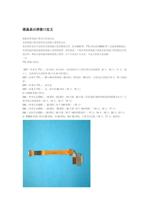
液晶显示屏接口定义液晶屏常见接口样式与区别方法从屏的接口样式简单区分屏接口类型的方法很多初学者对于如何区分屏的接口类型很是头疼,是LVDS屏,TTL屏还是RSDS屏?总是很难搞清出。
如何快速识别出液晶屏的接口类型则需要一些经验的,下面从屏的屏线接口的样式来对接口类型做出分类的介绍,帮助大家快速识别屏的接口类型。
以下方法是个人认识,不足之处请大家谅解。
(1)TTL屏接口样式:D6T(单6位TTL):31扣针,41扣针。
对应屏的尺寸主要为笔记本液晶屏(8寸,10寸,11寸,12寸),还有部分台式机屏15寸为41扣针接口。
S6T(双6位TTL):30+45针软排线,60扣针,70扣针,80扣针。
主要为台式机的14寸,15寸液晶屏。
D8T(单8位TTL):很少见S8T(双8位TTL):有,很少见80扣针(14寸,15寸)2)LVDS屏接口样式:D6L(单6位LVDS):14插针,20插针,14片插,30片插(屏显基板100欧姆电阻的数量为4个)主要为笔记本液晶屏(12寸,13寸,14寸,15寸)D8L(单8位LVDS):20插针(5个100欧姆)(15寸)S6L(双6位LVDS):20插针,30插针,30片插(8个100欧姆)(14寸,15寸,17寸)S8L(双8位LVDS):30插针,30片插(10个100欧姆电阻)(17寸,18寸,19寸,20寸,21寸)3)RSDS屏接口样式:50排线,双40排线,30+50排线。
主要为台式机(15寸,17寸)液晶屏。
这是笔记本用的20针lvds接口这是普通用的液晶显示器用点屏线:左边接驱动板,右边接液晶屏(20针与30针lvds接口相似)这里面都是lvds接口:有30针、20针的这些是41扣针接口(双排)这是60扣针接口(80扣针接口与这个相似)本贴来自天极网群乐社区--/group/review-9288206.html液晶屏接口定义(2008-01-18 18:09:43)孤影清风的BLOG20PIN单6定义:3.3V 3.3V1:电源2:电源3:地 4:地 5:R0- 6:R0+ 7:地 8:R1- 9:R1+ 10:地 11:R2- 12:R2+ 13:地 14:CLK- 15:CLK+ 16空 17空 18空 19 空 20空每组信号线之间电阻为(数字表100欧左右)指针表20 -100欧左右(4组相同阻值)20PIN双6定义:1:电源2:电源3:地 4:地 5:R0- 6:R0+ 7:R1- 8:R1+ 9:R2- 10:R2+ 11:CLK- 12:CLK+ 13:RO1- 14:RO1+ 15:RO2- 16:RO2+ 17:RO3- 18:RO3+19:CLK1- 20:CLK1+每组信号线之间电阻为(数字表100欧左右)指针表20 -100欧左右(8组相同阻值)20PIN单8定义:1:电源2:电源3:地 4:地 5:R0- 6:R0+ 7:地 8:R1- 9:R1+ 10:地 11:R2- 12:R2+ 13:地 14:CLK- 15:CLK+ 16:R3- 17:R3+每组信号线之间电阻为(数字表100欧左右)指针表20 -100欧左右(5组相同阻值)30PIN单6定义:1:空2:电源3:电源 4:空 5:空 6:空 7:空 8:R0- 9:R0+ 10:地 11:R1- 12:R1+ 13:地 14:R2- 15:R2+ 16:地 17:CLK- 18:CLK+ 19:地 20:空- 21:空 22:空 23:空 24:空 25:空 26:空 27:空 28空 29空 30空每组信号线之间电阻为(数字表100欧左右)指针表20 -100欧左右(4组相同阻值)30PIN单8定义:1:空2:电源3:电源 4:空 5:空 6:空 7:空 8:R0- 9:R0+ 10:地 11:R1- 12:R1+ 13:地 14:R2- 15:R2+ 16:地 17:CLK- 18:CLK+ 19:地 20:R3- 21:R3+ 22:地 23:空 24:空 25:空 26:空 27:空 28空 29空 30空每组信号线之间电阻为(数字表100欧左右)指针表20 -100欧左右(5组相同阻值)30PIN双6定义:1:电源2:电源3:地 4:地 5:R0- 6:R0+ 7:地 8:R1- 9:R1+ 10:地 11:R2- 12:R2+ 13:地 14:CLK- 15:CLK+ 16:地 17:RS0- 18:RS0+ 19:地 20:RS1- 21:RS1+ 22:地 23:RS2- 24:RS2+ 25:地 26:CLK2- 27:CLK2+30PIN双8定义:1:电源2:电源3:电源 4:空 5:空 6:空 7:地 8:R0- 9:R0+ 10:R1- 11:R1+ 12:R2- 13:R2+ 14:地 15:CLK- 16:CLK+ 17:地 18:R3- 19:R3+ 20:RB0- 21:RB0+ 22:RB1- 23:RB1+ 24:地 25:RB2- 26:RB2+ 27:CLK2-28:CLK2+ 29:RB3- 30:RB3+每组信号线之间电阻为(数字表100欧左右)指针表20 -100欧左右(10组相同阻值)一般14PIN、20PIN、30PIN为LVDS接口,25、31、40、41、60、70、75、80、100PIN接口为TTL接口,其中41PIN以下为单6位,60PIN以上为双六位屏50、80(50+30)PIN接口的为RSDS接口。
触摸显示器用户手册TOUCH MONITOR USER’S MANUAL(适用型号:WTM系列)(Applicable models: WTM Series)版本:2014修订版A重要请仔细阅读用户手册,掌握如何安全、有效地使用本产品。
尽管本公司已经尽最大努力使本手册提供最新信息,但是请注意本公司显示器规格仍会未经通知即进行变更,恕不另目录第1章 介绍 2 第2章 安装 3 第3章 装配 6 第4章 操作7 第5章 技术支持10 第6章 安全与维护11 第7章 联系我们13产品说明新的触摸显示器集anytouch触摸产品的可靠性能和触摸技术与显示屏设计领域的最新进展于一身。
这种性能组合可在用户与触摸显示屏之间提供自然的信息流动。
此触摸显示器带有一个 16.7M 彩色有源矩阵薄膜晶体管 LCD 面板,提供了优异的显示性能。
其它旨在增强此 LCD 显示器性能的功能包括:即插即用兼容性、屏幕显示 (OSD) 控件。
预防措施为了最大限度延长设备的使用寿命、确保用户安全以及预防风险,请采纳本用户手册中的所有警告、预防措施和维护建议。
有关更多信息,请参见“安全与维护”一章。
本手册包含正确设置和保养该设备的重要信息。
设置和开启新触摸显示器电源之前,请务必先通读本手册,特别是“安装”、“装配”和“操作”这几章。
产品特点1.即插即用触摸显示器,连接使用100~240V,50/60赫兹的通用的交流电源2.提供高清晰度分辨率3.全金属结构, 典雅大方且低调的外观设计,使内容更加脱颖而出4.提供背面VESA壁挂安装,四周侧孔安装,可调节支架安装,及定制支架安装等多种方式5.Windows XP /7 /8, Android , Linux, Mac OS X操作系统的完美支持技术参数型号WTM120 WTM150 WTM170 WTM190 WTM215 WTM270 VGA显示分1024 x 768 1024 x 768 1280 x 1024 1280 x 1024 1920 x 1080 1920 x 1080 辨率DVI显示分1024 x 768 1024 x 768 1280 x 1024 1280 x 1024 1920 x 1080 1920 x 1080 辨率VESA FDMI VESA,MIS-D,75,C VESA,MIS-D,100,C VESA,MIS-D,100,C VESA,MIS-D,100,C VESA,MIS-D,100,C VESA,MIS-E,C工作电压AC100V -240V (50/60Hz)输入电压DC12V*注:具体参数见相应的规格书打开触摸显示器的包装验证是否有以下项目VGA线*1、DVI线*1、电源适配器(12V)*1、电源线*1、USB连接线*1、安装支架*4、螺丝包*2、相应的驱动光盘、合格证、桌面支架(选配件)连接器面板与接口触摸显示器的连接1.用VGA视频电缆分别连接显示器的VGA输入连接器与VGA视频源;或用DVI视频电缆分别连接显示器的DVI输入连接器与DVI视频源。
REV.SPEC. NUMBER ISSUE DATEPAGETFT- LCDPRODUCT GROUPOF 28HEFEI BOE OPTOELECTRONICS TECHNOLOGYS8-*P0PROPRIETARY NOTETHIS SPECIFICATION IS THE PROPERTY OF BOE HF AND SHALL NOT BEREPRODUCED OR COPIED WITHOUT THE WRITTEN PERMISSION OF BOE HF AND MUST BE RETURNED TO BOE HF UPON ITS REQUESTITEM SUPPLIER SIGNATURE DATEPreparedReviewedApproved1 BUYER SUPPLIER HEFEI BOE Optoelectronics Technology CO., LTD FG-CodeBA104S01-300(ET104S0M-N10-3850)ITEM BUYER SIGNATURE DATES8- 2018-4-8BA104S01-300Product Specification Rev.P0BA104S01-300 Product SpecificationOF 28REVISION HISTORYS8-*2 REV.ECN No. DESCRIPTION OF CHANGESDATEPREPAREDP0Initial Release2018-4-8王兵P1 2018-6-12 王兵OF 28 S8-* 3BA104S01-300 Product SpecificationContentsNo. Items Page1.0 General Description *2.0 Absolute Maximum Ratings3.0 Electrical Specifications4.0 Optical Specifications5.0 Reliability Test6.0 Packing Information7.0 Product Label8.0 Handling & Cautions9.0 AppendixOF 28BA104S01-300 Product Specification S8-*4 1.0 GENERAL DESCRIPTION1.1 IntroductionBA104S01-300 is a color active matrix TFT LCD module using amorphous silicon TFT‘s (Thin Film Transistors) as an active switching devices. This module has a 10.4 inch diagonally measured active area with SVGAresolutions (800 horizontal by 600 vertical pixel array). Each pixel is divided into RED, GREEN, BLUE dots which are arranged in vertical stripe and this module can display 16.7M colors .1.2 Features● 0.5T Glass (Single ); ● Module Design● 6/ 8bits LVDS data input selection ● Thin and light weight● High luminance and contrast ratio, low reflection and wide viewing angle ● RoHS compliantSignal Input ConnectorBLU Input ConnectorDC/DC ConverterTFT LCD 800*600ICLED driverLED Light BarLVDS SignalLCD PowerVLEDTiming ControllerOF 28BA104S01-300 Product Specification S8-*5 ParameterSpecificationUnit RemarksActive Area 211.2(H)*158.4(V) mm Number Of Pixels 800(H)×600(V)pixels Pixel Pitch 0.264(H)×RGB ×0.264(V) mmPixel Arrangement Pixels RGB stripe arrangement Display Mode Normally White Display Colors 16.2M(8bits) colors 6+2Display Mode Transmissive modeSurface Treatment AG25(CF ),Clear (TFT ) Contrast Ratio 800:1(typ.) Viewing Angle(CR>10) 80/80/65/75(typ.) deg. Response Time 30(typ.) ms Color Gamut 55%Brightness300(min)/350(typ) cd/m2Brightness Uniformity 9 point: min 70% 9 point: typ 80%Power Consumption LCD: 0.58(Max.)(Black Pattern) BLU: 1.98W(Max.)watt Outline Dimension 236(H)*176.9(V)*5.6(typ)(LCM) mm Weight300(Max.)gram1.3 ApplicationMedical & Industrial application1.4 General SpecificationThe followings are general specifications at the ** ********<Table 1. LCD Module Specifications>OF 28BA104S01-300 Product Specification S8-*6 2.0 ABSOLUTE MAXIMUM RATINGSThe followings are maximum values which, if exceed, may cause faulty operation ordamage to the unit. The operational and non-operational maximum voltage and current values are listed in Table 2.< Table 3. Absolute Maximum Ratings>Note : 1) Temperature and relative humidity range are shown in the figure below.Wet bulb temperature should be 39 ℃ max. and no condensation of water.ParameterSymbol Min. Max. Unit RemarksPower SupplyLCD Module VDDVSS-0.33.9VTa = 25 ℃VLED VSS-0.343 V BLUILED - 25 mA Operating Temperature T OP -20 +70 ℃ Note 1Storage TemperatureT ST-30+80℃OF 28BA104S01-300 Product Specification S8-*7 3.0 ELECTRICAL SPECIFICATIONS3.1 TFT LCD Module< Table 4. LCD Module Electrical specifications > [Ta =25±2 ℃]Notes : 1. The supply voltage is measured and specified at the interface connector of LCM.The current draw and power consumption specified is for VBAT=3.8V, Frame rate f V =60Hz and Clock frequency = 156.8MHz. Test Pattern of power supply current a) Typ : Mosaic 8 x 6 Pattern(L0/L255) b) Max : Black2. The duration of rush current is about 2ms and rising time of Power Input is 1ms(min)ParameterSymbol ValuesUnit NotesMin. Typ. Max.Power Supply Voltage VDD 3.0 3.3 3.6 V Power Supply Current IDD 120 150 180 mA BLU Supply Voltage VLED 11.5 12 12.5 V BLU Supply Current ILED - 120 - mA Power Consumption PLCD 0.4 0.495 0.59 W BLU Power ConsumptionPBLU- -1.98WOF 28BA104S01-300 Product Specification S8-*8 3.2 Back-Light UnitTable 5. LED Driver Electrical Specifications >[Ta =25±2 ℃]Notes: 1. ILED=4*25mA=100mA ,4Parallel*6StringPLED = VLED ×ILED (Without LED converter transfer efficiency)2. The life time of LED, 30,000Hrs, is determined as the time at which luminance of the LED is 50% compared to that of initial value at the typical LED current on condition of continuous operating at 25 2°C.Parameter Symbol ValuesUnit NotesMin. Typ. Max. LED Supply Voltage VLED - 19.2 19.8 V VRP 300 mV Ripple LED Forward Current ILED - 25 - mA Note 1Power Consumption PLED - 1.921.98 W BLU on/off LevelBLU on 3 3.6 V BLU off 0 0..5 V PWMINLevelHigh Level 3 3.6 V Low Level 0 0.5 V Frequency F PWM 200 - 20K Hz Duty RatioD PWM 1 - 100 % LED Quantity QLED - 24 - EA LED Life TimeTLED30000- -HrsNote 2OF 28 S8-* 9BA104S01-300 Product Specification3.4 INPUT TERMINAL PIN ASSIGNMENTThis LCD employs two interface connections, a 20 pin ZIF connector is used for the LCD module electronics interface and a 5 pin ZIF connector is used for the internal backlight system.3.4.1 Pin assignment for LCD moduleConnector : MSB24013P20 _HA(STM) or equivalent< Table7. Pin Assignment for LCD Module Connector > Pin No. Symbol Description I/O1 VCC Power supply P2 VCC Power supply P3 GND Ground -4 SEL VCC:8Bits; GND/NC:6Bits I5 RIN0- LVDS signal input I6 RIN0+ LVDS signal input I7 GND Ground -8 RIN1- LVDS signal input I9 RIN1+ LVDS signal input I10 GND Ground -11 RIN2- LVDS signal input I12 RIN2+ LVDS signal input I13 GND Ground -14 CLKIN- LVDS clock input I15 CLKIN+ LVDS clock input I16 GND Ground -17 RIN3- LVDS signal input I18 RIN3+ LVDS signal input I19 NC No connection I20 NC/GND Test function -OF 28BA104S01-300 Product Specification S8-*10 Pin No Symbol Description Remarks1 NC No connection 2PWMLuminance control3 EN 3.3V-on / 0V-off4 GND Ground 5VLEDPower supply12V3.4.2 Pin assignment for LED BarConnector : MSB24038P5 (STM) or equivalent< Table8. Pin assignment for LED Bar >OF 28BA104S01-300 Product Specification S8-*11 ParameterSymbolMinTypMaxUnitConditionSupply currentI DD - 75 - mA LVDS DC specifications Differential input high threshold V TH - - +100 mV V IC =1.2VDifferential input low threshold V TL -100 - - mV LVDS common mode voltage V IC 0.7 - 1.6 V LVDS swing voltageV ID±100-±600mV3.5.2 DC Specification< Table11. DC Specification >LVCLKNLVCLKPLVCLKP-LVCLKN0VGNDV IDV ICV ID< LVDS V ID and V IC definition>OF 28 12OF 28BA104S01-300 Product SpecificationS8-* 13Item Symbol min typ max UNITLCD Frame Rate - - 60 - Hz Pixels Rate - 37.69 37.879 38.068 MHzTiming HorizontalHorizontal total time tHP - 1056 - t CLKHorizontal Active time tHadr800 t CLK Horizontal Back Porch tHBP88 t CLKHorizontal Front Porch tHFP 40 t CLK VerticalVertical total time tvp 628 t HVertical Active time tVadr 600 t HVertical Back Porch tVBP 23 t HVertical Front Porch tVFP 1 t HLane - 1 - Lane3.6 Interface timing Parameter< Table13. Timing Parameter >OF 28BA104S01-300 Product SpecificationS8-*14 ParameterValueUnits Min. Typ. Max. T1 0.1 - 5 (ms) T2 10 - 30 (ms) T3 5 - 100 (ms) T4 200 - - (ms) T5 200 - - (ms) T6 0 - 50 (ms) T7 0 - 10 (ms) T8500--(ms)[Ta =25±2 ℃]T7Interface Signal (LVDS/MIPI/eDP)Power for LEDPower Supply VDD90% 10%10%0V 90%T 1 T 2T 6 Valid video0VOFFOFFLED ONT 8T 3T 5Tcon Reset T 43.7 Power Sequence< Table15. Sequence Table >OF 28BA104S01-300 Product SpecificationS8-*4.2 Optical Specifications < Table16. Optical Table >15 4.0 OPTICAL SPECIFICATIONS4.1 OverviewThe test of optical specifications shall be measured in a dark room (ambient luminance ≤1lux and temperature = 25±2℃) with the equipment of Luminance meter system (Gonio meter system and TOPCON BM-5) and test unit shall be located at an approximate dista nce 50cm from the LCD surface at a viewing angle of θ and Φ equal to 0︒. We refer to θØ=0 (=θ3 ) as the 3 o’clock direction (the “right”), θØ=90 (= θ12 ) as the 12 O’clock direction (“upward”), θØ=180 (= θ9 ) as the 9 O’clock direction (“left”) and θØ=270(= θ6 ) as the 6 O’clock direction (“bottom”). While scanning θ and/or Ø, the center of the measuring spot on the Display surface shall stay fixed.Item Symbol Condition Min Typ. Max Unit Note luminance Bp θ=0°300 350 -- cd/m2 Note 1 Brightness Uniformity△Bp 70 80 -- %Note 2Viewing AngleθLCr≥10 70 80 -- degNote 3θR 70 80 -- ψT 55 65 -- ψB65 75 --Contrast Ratio Cr θ=0° FF=0° 600 800 - Note 4 Response TimeTr+Tf - 30 35 msNote 5Color Coordinate ofCIE1931Rx θ=0° 0.574 0.604 0.634 -Note 6Ry 0.296 0.326 0.356 Gx0.279 0.309 0.339 Gy 0.548 0.578 0.608 Bx 0.119 0.149 0.179 By 0.070 0.100 0.130 Wx 0.254 0.284 0.314 Wy0.290 0.320 0.350 NTSC Ratio NTSC CIE1931 5055 --% Note 7Polarization Direction of Front Polarizer PdF 45° degNote 8Polarization Direction of Rear Polarizer PdR45° DegGray inversion angle6点钟Note 9OF 28 S8-* 16BA104S01-300 Product SpecificationNote1:Luminance measurementThe test condition is at ILED=100mA and measured on the surface of LCD module at 25℃.●The data are measured after LEDs are lighted on for more than 5 minutes and LCM displays are fully white. The brightness is the center of the LCD. Measurement equipment CS2000 or similar equipments (Field of view:1deg,Distance:50cm)●Measuring surroundings: Dark room.●Measuring temperature: Ta=25℃.●Adjust operating voltage to get optimum contrast at the center of the display.●Measured value at the center point of LCD panel must be after more than 5 minutes while backlight turning on.Note2:Uniformity●The test condition is at ILED=100mA and measured on the surface of LCD module at 25℃.●Measurement equipment:CS2000 or similar equipments●The luminance uniformity is calculated by using following formula:●△Bp = Bp (Min.) / Bp (Max.)×100 (%)●Bp (Max.) = Maximum brightness in 9 measured spots●Bp (Min.) = Minimum brightness in 9 measured spots.OF 28BA104S01-300 Product SpecificationS8-*17 Note 3:The definition of Viewing AngleRefer to the graph below marked by θ and Ф.Note4:ThedefinitionofContrastRatio (Test LCM using CS2000 or similar equipments):Luminance When LCD is at “White” stateContrast Ratio(CR)=Luminance When LCD is at “Black” state(Contrast Ratio is measured in optimum common electrode voltage)Note5:DefinitionofResponse time.(Test LCD using DMS501 or similar equipments):The output sign also photo detector are measured when the input sign also are changed from “black ” to “white”(Voltage falling time)and from “white” to “black” (Voltage rising time), respectively .The response time is defined as the time interval between the 10% and 90% of amplitudes . Refer to fi gures below.Response time of gray to gray:Measurement equipment: DMS501 or similar equipments.Test method: we define 8 grays L0-L7,the grays of L0-L7 were defined as:0,36,73, 109, 146, 182, 219, 255. Theoutputsignalsofphotodetectoraremeasuredwhentheinputsignalsarechanged from “Lx” to “Ly”, x, y= [0, 7]. The response time is defined as the time interval between the 10% and 90% of amplitudes. The result of the test can be noted as below:L0 L1 L2 L3 L4 L5 L6 L7 L0 L1 L2 L3 L4 L5 L6 L7OF 28 S8-* 18BA104S01-300 Product SpecificationNote 6: Color Coordinates of CIE 1931The test condition is at ILED=100mA and measured on the surface of LCD module at 25℃. Measurement equipment:CS2000 or similar equipmentsThe Color Coordinate (CIE 1931) is the measurement of the center of the display shown in below figure. Note 7: Definition of Color of CIE Coordinate and NTSC Ratio.Note 8: Polarization Direction Definition●Viewing direction is normal user viewing direction which is vertical to the display surface●The polarizer which is closer to viewer is defined as Front Polarizer●The polarizer which is on the rear side of viewer is defined as Rear Polarizer●The X axis is defined as parallel line to top & bottom sidelines of the Active Area●PdF which is marked in blue arrow is polarization degree of Front polarizer●PdB which is marked in red arrow is polarization degree of Back polarizer●The polarization degree parameter must be indicated in range of 0deg to 180deg according to above definitionOF 28BA104S01-300 Product SpecificationS8-*19 Note 9: Definition of gray inversion angle ●Refer to the graph of note 9. ●Using luminance test method. ●Test pattern : 128 gray●If the viewing direction is 12 o’clock ,then test the luminance while θ=-60°,θ=-50°, θ=-40°, θ=-30°, θ=-20°, θ=-10°, θ=0°, θ=10°, θ=20°, θ=30°, θ=40°, θ=-50°, θ=60°. The luminance test as figure below:50100150200-100-5050100-60-50-40-30-20-10010OF 28 S8-* 20BA104S01-300 Product Specification5.0 RELIABLITY TESTThe Reliability test items and its conditions are shown in below.<Table 17. Reliability Test Parameters >No Test Items Conditions1 High temperature storage test 80℃,240hr2 Low temperature storage test -30℃,240hr3 High temperature & high humidity(operation test) 60℃,90%RH,240hr4 Low temperature operation test -20℃,240hr5 High temperature operation test 70℃,240hr6 Thermal Shock Test -40℃~85℃,1hr/cycle,100cycle7 ALT -10℃~65℃,0%~93%,24hr/cycle,10 cycle8 PCT 121℃,100%RH,2atm,12hr9 ESD 150pF,330Ω,±6kV(Contact),±8kV(Air)10 Packing VIB 1.47G,1-200hz,X,Y,±Z,30min/AxisOF 28BA104S01-300 Product Specification S8-*21 6.1 Packing Note(产品形态:LCM)• Box Dimension: 500mm(W) x 400mm(D) x 300mm(H) • Package Quantity in one Box: 28pcsPacking procedure:6.0 PACKING INFORMATION(产品形态: )-.Put 1pcs Panel into PE Bag Crimp PE Bag opening-. Insert 1pcs panel horizontally into the slot -. 28pcs Panel /EPE Box-. Put 1pcs EPE cover upon EPE box -.Put EPE Box& EPE cover into Inner Box -. 28pcs Panel /Inner Box-. 4 layers/ Pallet -. 4 boxes/ Layer-. 448pcs Panel / PalletOF 28BA104S01-300 Product SpecificationS8-* 226.2 Box label (产品形态: )• Label Size :115mm*55mm• ContentsModel : LCMQ`ty : 28pcs/BoxSerial No. : Box Serial No. as shown below.Date : Packing DateFG Code : FG Code of ProductXXXXXXXXXXXXX 2820XX / XX/ XX xxxx1 23 45No. 1 2 3 4 5 6 7 8 9 10 11 12 13 Code X X S 3 1 8 B 0 0 0 1 H D GBN Grade B3 Year Month Rev Serial number BA104S01-300OF 28BA104S01-300 Product SpecificationS8-*7.0 Product LabelBOE MDL ID rule123 4Label Size: 48mmx12mmx0.08mm, 44-92310071. Customer Code2. MDL ID bar code3. MDL ID4. FG-CODE First 12 digitsNo. 1 2 3 4 5 6 7 8 9 10 11 121314151617Code X X S 3 8 3 2 D 8 5 0 0 0 0 0 2 1 GBN Grade B3 Year Month Day FG Code last four digits Serial number23OF 28 S8-* 24BA104S01-300 Product Specification8.0 Handling & Cautions8.1 Mounting Method● The panel of the LCD consists of two thin glasses with polarizers which easily getdamaged. So extreme care should be taken when handling the LCD.● Excessive stress or pressure on the glass of the LCD should be avoided. Care must betaken to insure that no torsional or compressive forces are applied to the LCD unitwhen it is mounted.● If the customer's set presses the main parts of the LCD, the LCD may show the abnormaldisplay. But this phenomenon does not mean the malfunction of the LCD and should bepressed by the way of mutual agreement.● To determine the optimum mounting angle, refer to the viewing angle range in thespecification for each model.● Mount a LCD module with the specified mounting parts.8.2 Caution of LCD Handling and Cleaning●Since the LCD is made of glass, do not apply strong mechanical impact or static loadonto it. Handling with care since shock, vibration,and careless handling may seriouslyaffect the product. If it falls from a high place or receives a strong shock, the glass maybe broken.● The polarizers on the surface of panel are made from organic substances. Be verycareful for chemicals not to touch the polarizers or it leads the polarizers to be deteriorated.● If the use of a chemical is unavoidable, use soft cloth with solvent(recommended below)to clean the LCD‘s surface with wipe lightly.-IPA(Isopropyl Alcohol), Ethyl Alcohol, Trichlorotriflorothane● Do not wipe the LCD's surface with dry or hard materials that will damage the polarizersand others. Do not use the following solvent.-Water, Ketone, Aromatics● It is recommended that the LCD be handled with soft gloves during assembly, etc. Thepolarizers on the LCD's surface are vulnerable to scratch and thus to be damaged bysharp particles.● Do not drop water or any chemicals onto the LCD's surface.● A protective film is supplied on the LCD and should be left in place until the LCD isrequired for operation.● The ITO pad area needs special careful caution because it could be easily corroded.Do not contact the ITO pad area with HCFC,Soldering flux,Chlorine,Sulfur,saliva orfingerprint. To prevent the ITO corrosion, customers are recommended that the ITOarea would be covered by UV or silicon.OF 28 S8-*BA104S01-300 Product Specification258.3 Caution Against Static Charge● The LCD modules use C-MOS LSI drivers, so customers are recommended that any unused input terminal would be connected to Vdd or Vss, do not input any signals beforepower is turn on, and ground you body, work/assembly area, assembly equipments toprotect against static electricity.● Remove the protective film slowly, keeping the removing direction approximate30-degree not vertical from panel surface, If possible, under ESD control device likeion blower, and the humidity of working room should be kept over 50%RH to reduce therisk of static charge.● Avoid the use work clothing made of synthetic fibers. We recommend cotton clothing orother conductivity-treated fibers.● In handling the LCD, wear non-charged material gloves. And the conducting wrist to theearth and the conducting shoes to the earth are necessary.8.4 Caution For operation● It is indispensable to drive the LCD within the specified voltage limit since the higherVoltage than the limit causes the shorter LCD's life. An electro-chemical reaction due toDC causes undesirable deterioration of the LCD so that the use of DC drive should avoid.● Do not connect or disconnect the LCD to or from the system when power is on.● Never use the LCD under abnormal conditions of high temperature and high humidity.● When expose to drastic fluctuation of temperature (hot to cold or cold to hot),theLCD may be affected; Specifically, drastic temperature fluctuation from cold to hot ,produces dew on the LCD's surface which may affect the operation of the polarizer and the LCD.● Response time will be extremely delayed at lower temperature than the operatingtemperature range and on the other hand at higher temperature LCD may turn black attemperature above its operational range. However those phenomena do not meanmalfunction or out of order with the LCD. The LCD will revert to normal operation oncethe temperature returns to the recommended temperature range for normal operation.● Do not display the fixed pattern for a long time because it may develop image stickingdue to the LCD structure. If the screen is displayed with fixed pattern, use a screen saver.OF 28S8-*BA104S01-300 Product Specification268.5 Packaging●Modules use LCD element, and must be treated as such.-Avoid intense shock and falls from a height.-To prevent modules from degradation, do not operate or store them exposed directly to sunshine or high temperature/humidity for long periods.8.6 Storage● A slight dew depositing on terminals is a cause for electro-chemical reaction resultingin terminal open circuit. Relative humidity of the environment should therefore be keptbelow 60%RH.●Original protective film should be used on LCD’s surface (polarizer). Adhesive typeprotective film should be avoided, because it may change color and/or properties ofthe polarizers.● Do not store the LCD near organic solvents or corrosive gasses.● Keep the LCD safe from vibration, shock and pressure.● Black or white air-bubbles may be produced if the LCD is stored for long time in thelower temperature or mechanical shocks are applied onto the LCD.● In the case of storing for a long period of time for the purpose or replacement use,the following ways are recommended.-Store in a polyethylene bag with sealed so as not to enter fresh air outside in it.-Store in a dark place where neither exposure to direct sunlight nor light is.-Keep temperature in the specified storage temperature range.-Store with no touch on polarizer surface by the anything else. If possible, store the LCDin the packaging situation LCD when it was delivered.8.7 Safety● For the crash damaged or unnecessary LCD, it is recommended to wash off liquid crystalby either of solvents such as acetone and ethanol an should be burned up later.● In the case the LCD is broken, watch out whether liquid crystal leaks out or not. If yourhands touch the liquid crystal, wash your hands cleanly with water an soap as soonas possible.● If you should swallow the liquid crystal, first, wash your mouth thoroughly with water,then drink a lot of water and induce vomiting, and then, consult a physician.● If the liquid crystal should get in your eyes, flush your eyes with running water for atleast fifteen minutes.● If the liquid crystal touches your skin or clothes, remove it and wash the affected partof your skin or clothes with soap and running water.27OF 28 S8-*BA104S01-300 Product Specification9.0 APPENDIXMechanical DrawingDrawing Attachment: FrontBA104S01-300 Product SpecificationMechanical DrawingDrawing Attachment: Back。
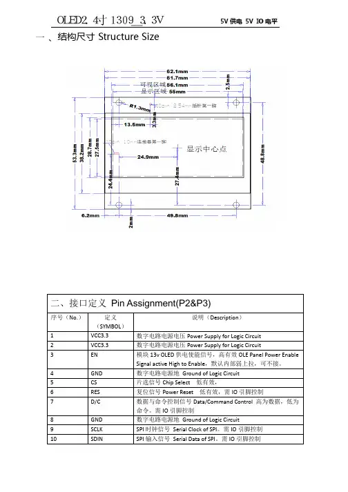
、结构尺寸StructureSize 一5V 供电5V IO 电平二、接口定义Pin Assignment(P2&P3)序号(No.)定义(SYMBOL )说明(Description )1VCC3.3数字电路电源电压Power Supply for Logic Circuit 2VCC3.3数字电路电源电压Power Supply for Logic Circuit 3EN 模块13v OLED 供电使能信号,高有效OLE Panel Power Enable Signal active High to Enable ,默认内部弱上拉,可不接。
4GND 数字电路电源地Ground of Logic Circuit 5CS 片选信号Chip Select 低有效,6RES 复位信号Power Reset 低有效,需IO 引脚控制7D/C 数据与命令控制信号Data/Command Control 高为数据,低为命令。
需IO 引脚控制8GND 数字电路电源地Ground of Logic Circuit 9SCLK SPI 时钟信号Serial Clock of SPI 。
需IO 引脚控制10SDIN SPI 输入信号Serial Data of SPI 。
需IO 引脚控制OLED2.4寸1309_3.3V一、产品介绍General SpecificationsDiagonal Size尺寸 2.4”Color颜色Yellow、Green、Blue、WhiteType类型MonochromePixel Number分辨率128x64Module Size(mm)模组尺寸62.1×53.3×9Active Size(mm)显示区域55.01×27.49Driver IC驱动IC SSD1309Interface接口4_Wire SPISupply Voltage供电电压 3.3VVoltage Range建议电压范围 1.65V~3.3VMax Voltage最大极限电压4VMin Voltage最小极限电压 1.65VView Angle视角>160degree全视角Contrast对比度>10000:1Brightness(cd/m2)亮度(绿色)120(Typ)@13V(20000Hours)Power功耗由点亮的像素决定30%像素点亮<260mw50%像素点亮<345mw100%像素点亮(实际使用中用不到)<515mwBrightness(cd/m2)(黄色)80(Typ)@13V(15000Hours)Power功耗由点亮的像素决定30%像素点亮<260mw50%像素点亮<380mw100%像素点亮(实际使用中用不到)<590mwBrightness(cd/m2)(白色)80(Typ)@13V(30000Hours)Power功耗由点亮的像素决定30%像素点亮<300mw50%像素点亮<440mw100%像素点亮(实际使用中用不到)<690mwBrightness(cd/m2)(蓝色)80(Typ)@13V(15000Hours)Power功耗由点亮的像素决定30%像素点亮<325mw50%像素点亮<470mw100%像素点亮(实际使用中用不到)<720mwWeight(g)重量8.6Assembly连接方式10Pin1.0mm FPC Connector and2.54mm Metal pins四、SPI接口特性SPI Timing Characteristics。
( V ) Preliminary Specifications( ) Final SpecificationsModule 10.4 Inch Color TFT-LCD Model Name G104STN01.0Customer Date Checked &Approved by Approved by DateGrace Hung 2013/08/16 Prepared byJohnson Lin 2013/08/16 General Display Business Division / AU Optronics corporationContents1. Operating Precautions (4)2. General Description (5)2.1 Display Characteristics (5)2.2 Optical Characteristics (6)3. Functional Block Diagram (9)4. Absolute Maximum Ratings (10)4.1 Absolute Ratings of TFT LCD Module (10)4.2 Absolute Ratings of Environment (10)5. Electrical Characteristics (11)5.1 TFT LCD Module (11)5.2 Backlight Unit (13)6. Signal Characteristics (14)6.1 Pixel Format Image (14)6.2 Scanning Direction (14)6.3 TFT-LCD Interface Signal Description (15)6.4 The Input Data Format (16)6.5 TFT-LCD Interface Timing (17)6.6 Power ON/OFF Sequence (18)7. Connector & Pin Assignment (19)7.1 TFT-LCD Signal (CN1): LVDS Connector (19)7.2 LED Backlight Unit (CN2): Driver Connector (19)7.3 LED Backlight Unit (CN4): Light bar Connector (19)8. Reliability Test Criteria (20)9. Mechanical Characteristics (21)9.1 LCM Outline Dimension (Front View) (21)9.2 LCM Outline Dimension (Rear View) (22)10. Label and Packaging (23)10.1 Shipping Label (on the rear side of TFT-LCD display) (23)10.2 Carton Package (23)11 Safety (25)11.1 Sharp Edge Requirements (25)11.2 Materials (25)11.3 Capacitors (25)11.4 National Test Lab Requirement (25)Record of RevisionVersion and Date Page Old description New Description1. Operating Precautions1) Since front polarizer is easily damaged, please be cautious and not to scratch it.2) Be sure to turn off power supply when inserting or disconnecting from input connector.3) Wipe off water drop immediately. Long contact with water may cause discoloration orspots.4) When the panel surface is soiled, wipe it with absorbent cotton or soft cloth.5) Since the panel is made of glass, it may be broken or cracked if dropped or bumped onhard surface.6) To avoid ESD (Electro Static Discharde) damage, be sure to ground yourself before handlingTFT-LCD Module.7) Do not open nor modify the module assembly.8) Do not press the reflector sheet at the back of the module to any direction.9) In case if a module has to be put back into the packing container slot after it was takenout from the container, do not press the center of the LED light bar edge. Instead, press at the far ends of the LED light bar edge softly. Otherwise the TFT Module may be damaged.10) At the insertion or removal of the Signal Interface Connector, be sure not to rotate nortilt the Interface Connector of the TFT Module.11) TFT-LCD Module is not allowed to be twisted & bent even force is added on module in a veryshort time. Please design your display product well to avoid external force applying to module by end-user directly.12) Small amount of materials without flammability grade are used in the TFT-LCD module. TheTFT-LCD module should be supplied by power complied with requirements of Limited Power Source (IEC60950 or UL1950), or be applied exemption.13) Severe temperature condition may result in different luminance, response time and lampignition voltage.14) Continuous operating TFT-LCD display under low temperature environment may acceleratelamp exhaustion and reduce luminance dramatically.15) The data on this specification sheet is applicable when LCD module is placed in landscapeposition.16) Continuous displaying fixed pattern may induce image sticking. It’s recommended to usescreen saver or shuffle content periodically if fixed pattern is displayed on the screen.2. General DescriptionThis specification applies to the Color Active Matrix Liquid Crystal Display G104STN01.0composed of a TFT-LCD display, a driver and power supply circuit, and a LED backlight system. The screen format is intended to support SVGA (800(H) x 600(V)) screen and 16.2M (RGB 8-bits) or 262k colors (RGB 6-bits).LED driving board for backlight unit is included in G104STN01.0 and the LED unit is replaceable. All input signals are LVDS interface and compatible with G104SN02 V2.G104STN01.0 designed with wide viewing angle; wide temperature and long life LED backlight is well suited for industial applications. G104STN01.0 is a RoHS product.2.1 Display CharacteristicsThe following items are characteristics summary on the table under 25 ℃ condition: ItemsUnitSpecifications Screen Diagonal [inch] 10.4Active Area [mm] 211.2 (H) x 158.4 (V) Pixels H x V 800 x 3(RGB) x 600 Pixel Pitch [mm] 0.264 x 0.264 Pixel Arrangement R.G.B. Vertical Stripe Display ModeTN, Normally White Nominal Input Voltage VDD [Volt] 3.3 (typ.) Typical Power Consumption [Watt] 2.88WAll black pattern Weight [Grams] 365(Typ.)Physical Size [mm] 243.0(H) x 184.0(V) x 6.5(D)(Typ.) Electrical Interface 1 channel LVDS Surface Treatment Anti-glare, Hardness 3H Support Color16.2M / 262K colors Temperature Range OperatingStorage (Non-Operating) [o C] [o C]-20 to +80 -20 to +80 RoHS ComplianceRoHS Compliance2.2 Optical CharacteristicsThe optical characteristics are measured under stable conditions at 25 (Room Temperature):℃Item Unit Conditions Min. Typ. Max. RemarkWhite Luminance[cd/m2] I F = 50mA/1 LED Line (center point) 300 400 -1 Uniformity % 5 Points 65 75 -2,3 Contrast Ratio500 700 - 4[msec]Rising - 10 20 [msec] Falling- 5 15 Response Time[msec] Raising + Falling - 15 35 5 [degree] [degree] Horizontal (Right) CR = 10 (Left) 70 70 80 80 - - Viewing Angle[degree] [degree]Vertical (Upper) CR = 10 (Lower) 50 60 60 70 - - 6 Red x - TBD - Red y - TBD - Green x- TBD - Green y - TBD - Blue x - TBD - Blue y - TBD - White x 0.28 0.31 0.34 Color / ChromaticityCoordinates (CIE 1931)White y0.30 0.33 0.36 Color Gamut%50-Note 1: Measurement method Equipment Pattern Generator, Power Supply, Digital Voltmeter, Luminance meter (SR_3 or equivalent) Aperture1with 50cm viewing distance ∘Test Point CenterEnvironment < 1 luxModule Driving EquipmentNote 2: Definition of 5 points position (Display active area: 211.2mm (H) x 158.4mm (V))Note 3: The luminance uniformity of 5 points is defined by dividing the minimum luminance values by the maximum test point luminanceNote 4: Definition of contrast ratio (CR):Note 5: Definition of response time:The output signals of photo detector are measured when the input signals are changed from “White” to “Black” (falling time) and from “Black” to “White” (rising time), respectively. The response time interval isNote 6: Definition of viewing angleViewing angle is the measurement of contrast ratio 10, at the screen center, over a 180° horizontal and ≧180° vertical range (off-normal viewing angles). The 180° viewing angle range is broken down as below: 90° (θ) horizontal left and right, and 90° (Φ) vertical high (up) and low (down). The measurement direction is typically perpendicular to the display surface with the screen rotated to its center to develop the desiredMinimum Brightness of five pointsδW9 = Maximum Brightness of five points Contrast ratio (CR)=Brightness on the “White” stateBrightness on the “Black” statemeasurement viewing angle.3. Functional Block DiagramThe following diagram shows the functional block of the 10.4 inch color TFT/LCD module:4. Absolute Maximum Ratings4.1 Absolute Ratings of TFT LCD ModuleItem Symbol Min Max Unit Logic/LCD Drive Voltage Vin -0.3 +4.0 [Volt]4.2 Absolute Ratings of EnvironmentItem Symbol Min Max Unit Operating Temperature TOP -20 +80 [o C] Operation Humidity HOP 5 95 [%RH] Storage Temperature TST -20 +80 [o C] Storage Humidity HST 5 95 [%RH] Note: Maximum Wet-Bulb should be 39℃ and no condensation.5. Electrical Characteristics 5.1 TFT LCD Module5.1.1 Power SpecificationSymbol Parameter Min Typ Max Units RemarkVDD Logic/LCD Input Voltage 3.0 3.3 3.6 [Volt]I VDD LCD Input Current - 320 - [mA]VDD=3.3V at 60 HZ, all Black PatternP VDD LCD Power comsumption - - 1.5 [Watt] VDD=3.3V at 60 HZ, all Black Pattern I rush LCDLCD Inrush Current-1.06-[A] Note 1; VDD=3.3VBlack Pattern, Rising time=470usVDD rpAllowable Logic/LCDDrive Ripple Voltage- -100 [mV] p-pVDD=3.3V at 60 HZ, all Black PatternNote 1: Measurement condition:VDD rising time0V3.3V5.1.2 Signal Electrical CharacteristicsInput signals shall be low or Hi-Z state when VDD is off.Note: LVDS Signal Waveform.Symbol ItemMin. Typ.Max. Unit RemarkVTH Differential Input High Threshold - - 100 [mV] VCM=1.2V VTL Differential Input Low Threshold 100 - - [mV] VCM=1.2V |VID |Input Differential Voltage100 400 600 [mV] VICMDifferential Input Common Mode Voltage1.1251.251.375[V]VTH/VTL=+-100mV5.2 Backlight Unit5.2.1 Parameter guideline for LED backlightFollowing characteristics are measured under a stable condition using a inverter at 25℃. (Room Temperature): Symbol Parameter Min.Typ.Max.Unit RemarkVCC Input Voltage 10.8 12 12.6 [Volt]I VCC Input Current - 0.32 - [A] 100% PWM DutyP VCC Power Consumption - 2.88 - [Watt] 100% PWM DutyF PWM Dimming Frequency 200 - 20K [Hz]Swing Voltage 3 3.3 5.5 [Volt]Dimming duty cycle 5 - 100 %I F LED Forward Current-50 -[mA] Ta = 25o C- 27.2 - [Volt]I F = 50mA, Ta = -30o C V F LED Forward Voltage- 26.4 28.8 [Volt]I F = 50mA, Ta = 25o C- 25.6 - [Volt]I F = 50mA, Ta = 85o C P LED LED Power Consumption- 2.72 - [Watt]Operation Life 50,000 - - Hrs I F=50mA, Ta= 25o CNote 1: Ta means ambient temperature of TFT-LCD module.Note 2: VCC, I VCC, I rush LED, P VCC are defined for LED backlight.(100% duty of PWM dimming)Note 3: I F, V F are defined for one channel LED. There are two LED channel in back light unit.Note 4: If G104STN01.0 module is driven by high current or at high ambient temperature & humidity condition. The operating life will be reduced.Note 5: Operating life means brightness goes down to 50% initial brightness. Minimum operating life time is estimated data.6. Signal Characteristics6.1 Pixel Format ImageFollowing figure shows the relationship between input signal and LCD pixel format.1st2nd799th800th1stLine600thLin6.2 Scanning DirectionThe following figures show the image seen from the front view. The arrow indicates the direction of scan.Fig. 1 Normal scan (Pin4, DPS = Low or NC) Fig. 2 Reverse scan (Pin4, DPS = High)6.3 TFT-LCD Interface Signal DescriptionThe module using a LVDS receiver embaded in AUO’s ASIC. LVDS is a differential signal technology for LCD interface and a high-speed data transfer device.Input Signal Interface Pin No. SymbolDescription 1 VDD Power Supply, 3.3V (typical) 2 VDD Power Supply, 3.3V (typical) 3 GND Ground4 DPS Reverse Scan Function [H: Enable; L/NC: Disable]5 RxIN0-6 RxIN0+ LVDS receiver signal channel 0LVDS Differential Data Input (R0, R1, R2, R3, R4, R5, G0)7 GND Ground8 RxIN1- 9 RxIN1+ LVDS receiver signal channel 1LVDS Differential Data Input (G1, G2, G3, G4, G5, B0, B1) 10 GND Ground11 RxIN2- 12 RxIN2+ LVDS receiver signal channel 2LVDS Differential Data Input (B2, B3, B4, B5, DE)13 GNDGround14 RxCLKIN- 15 RxCLKIN+ LVDS receiver signal clock 16 GND Ground17 RxIN3- 18 RxIN3+ LVDS receiver signal channel 3, pin17=3.3V&pin 18=GND for 6bit LVDS InputLVDS Differential Data Input (R6, R7, G6, G7, B6, B7, RSV)19 RSVReserved for AUO internal test. Please treat it as NC.20SEL68 6/8bits LVDS data input selection [H: 8bits L/NC: 6bit]Note 1: Input Signals shall be in low status when VDD is off.Note 2: High stands for “3.3V”, Low stands for “0V”, NC stands for “No Connection”. Note 3: RSV stands for “Reserved”.6.4 The Input Data Format6.4.1 SEL68SEL68 =“Low” or “NC” for 6 bits LVDS InputSEL68 = “High” for 8 bits LVDS InputNote1: Please follow PSWG.Note2: R/G/B data 7:MSB, R/G/B data 0:LSBSignal Name DescriptionRemarkR7R6R5R4R3R2R1R0Red Data 7 Red Data 6 Red Data 5 Red Data 4 Red Data 3 Red Data 2 Red Data 1 Red Data 0 Red-pixel DataFor 8Bits LVDS input MSB: R7 ; LSB: R0For 6Bits LVDS input MSB: R5 ; LSB: R0G7G6G5G4 G3G2G1 G0Green Data 7 Green Data 6 Green Data 5 Green Data 4Green Data 3 Green Data 2 Green Data 1Green Data 0 Green-pixel DataFor 8Bits LVDS input MSB: G7 ; LSB: G0For 6Bits LVDS input MSB: G5 ; LSB: G0B7 B6 B5 B4 B3 B2 B1 B0 Blue Data 7 Blue Data 6 Blue Data 5 Blue Data 4 Blue Data 3 Blue Data 2 Blue Data 1 Blue Data 0 Blue-pixel DataFor 8Bits LVDS input MSB: B7 ; LSB: B0For 6Bits LVDS input MSB: B5 ; LSB: B0 RxCLKIN LVDS Data ClockDE Data Enable SignalWhen the signal is high, the pixel data shall be valid to be displayed.Note: Output signals from any system shall be low or Hi-Z state when VDD is off.NS-like format6.5 TFT-LCD Interface Timing6.5.1 Timing CharacteristicsSignal Symbol Min. Typ. Max. Unit Clock Frequency 1/ T Clock 30 40 50 MHzPeriod T V 608 628 1024 Active T VD -- 600-- Vertical SectionBlankingT VB 8 28 424 T Line Period T H 960 1056 1060Active T HD -- 800 -- Horizontal SectionBlankingT HB 160 256 260 T ClockFrame RateF 506075Hz Note : DE mode.6.5.2 Input Timing DiagramDOTCLKDEHT HBDET VDInput Timing Definition ( DE Mode)Input Data Invaild Data Invaild Data6.6 Power ON/OFF SequenceVDD power and lamp on/off sequence is as below. Interface signals are also shown in the chart. Signals from any system shall be Hi-Z state or low level when VDD is off.Power ON/OFF sequence timingValue UnitsParameterMin. Typ. Max.T10.5 - 10 [ms]T2 30 40 50 [ms]T3 200 -- -- [ms]T4 0.5 -- 10 [ms]T5 10 - - [ms]T6 10 - - [ms]T7 0 - - [ms]T8 10 - - [ms]T9 -- -- 10 [ms]T10 110 -- -- [ms]T11 0 16 50 [ms]T12 - - 10 [ms]T13 1000 - - [ms]The above on/off sequence should be applied to avoid abnormal function in the display. Please make sure to turn off the power when you plug the cable into the input connector or pull the cable out of the connector.7. Connector & Pin AssignmentPhysical interface is described as for the connector on module. These connectors are capable of accommodating the following signals and will be following components.7.1 TFT-LCD Signal (CN1): LVDS ConnectorConnector Name / Designation Signal ConnectorManufacturer STM or compatibleConnector Model Number MSB24013P20HA or compatibleAdaptable Plug P24013P20 or compatiblePin No. Symbol Pin No. Symbol1 VDD2 VDD3 GND4 DPS5 RxIN0-6 RxIN0+7 GND 8 RxIN1-9 RxIN1+ 10 GND11 RxIN2- 12 RxIN2+13 GND 14 RxCKIN-15 RxCKIN+ 16 GND17 RxIN3- 18 RxIN3+19 RSV 20 SEL687.2 LED Backlight Unit (CN2): Driver ConnectorConnector Name / Designation Lamp ConnectorManufacturer ENTERY or compatibleConnector Model Number 3808K-F05N-12R or compatibleMating Model Number H208K–P05N-02B or compatiblePin No. symbol descriptionPin1 VCC 12V inputPin2 GND GNDPin3 On/OFF 5V-ON,0V-OFFPin4 Dimming PWMPin5 NA7.3 LED Backlight Unit (CN4): Light bar ConnectorConnector Name / Designation Lamp ConnectorManufacturer ENTERY or compatibleConnector Model Number H208K–P03N-02B or compatibleMating Model Number(CN3) 3808K-F03N-12R or compatiblePin No. symbol description ColorPin1 H LED anode RedPin2 L LED cathode WhitePin3 L LED cathode Black8. Reliability Test CriteriaItems Required Condition Note Temperature Humidity Bias 40℃, 90%RH, 300 hoursHigh Temperature Operation 80℃, 300 hoursLow Temperature Operation -20℃, 300 hoursHot Storage 80,℃ 300 hoursCold Storage -20,℃ 300 hoursThermal Shock Test -20/℃ 30 min, 60/℃ 30 min, 100cycles, 40℃minimun ramp rateHot Start Test 80℃/ 1Hr min. power on/off per 5 minutes, 5 timesCold Start Test -20℃/ 1Hr min. power on/off per 5 minutes, 5 timesShock Test (Non-Operating) 50G, 20ms, Half-sine wave, ( ±X, ±Y, ±Z)Vibration Test (Non-Operating) 1.5G, (10~200Hz, Sine wave)30 mins/axis, 3 direction (X, Y, Z)On/off test On/10 sec, Off/10 sec, 30,000 cyclesESD Contact Discharge: ± 8KV, 150pF(330Ω ) 1sec, 8 points, 25 times/ pointAir Discharge: ± 15KV, 150pF(330Ω ) 1sec, 8 points, 25 times/ pointNote 1EMI 30-230 MHz, limit 40 dBu V/m, 230-1000 MHz, limit 47 dBu V/mNote1: According to EN61000-4-2, ESD class B: Some performance degradation allowed. No data lost Self-recoverable. No hardware failures.Note2:Water condensation is not allowed for each test items.Each test is done by new TFT-LCD module. Don’t use the same TFT-LCD module repeatedly for reliability test. The reliability test is performed only to examine the TFT-LCD module capability.To inspect TFT-LCD module after reliability test, please store it at room temperature and room humidity for 24 hours at least in advance.G104STN01.09. Mechanical Characteristics工业液晶屏:www.hzxuhong.com杭州旭虹科技有限公司G104STN01.09.2 LCM Outline Dimension (Rear View)工业液晶屏:www.hzxuhong.com杭州旭虹科技有限公司G104STN01.010. Label and Packaging10.1 Shipping Label (on the rear side of TFT-LCD display)10.2 Carton PackageNote:Max capacity :20 TFT-LCD module per cartonMax weight: 11.5 kg per cartonOutside dimension of carton: 477mm(L)* 290mm(W)*360mm(H)Pallet size : 1180 mm * 980 mm * 135mmBox stackedModule by air :(2 *4) *4 layers ,one pallet put 32 boxes ,total 640pcs module Module by sea :(2 *4) *4 layers + (2 *4) *1 layers , two pallet put 40 boxes ,total 800pcs module Module by sea_HQ :(2 *4) *4 layers+(2 *4) *2 layers, two pallet put 48 boxes, total 960pcs module工业液晶屏:www.hzxuhong.com杭州旭虹科技有限公司杭州旭虹科技有限公司11 Safety11.1 Sharp Edge RequirementsThere will be no sharp edges or comers on the display assembly that could cause injury.11.2 Materials11.2.1 ToxicityThere will be no carcinogenic materials used anywhere in the display module. If toxic materials are used, they will be reviewed and approved by the responsible AUO toxicologist.11.2.2 FlammabilityAll components including electrical components that do not meet the flammability grade UL94-V1 in the module will complete the flammability rating exception approval process.The printed circuit board will be made from material rated 94-V1 or better. The actual UL flammability rating will be printed on the printed circuit board.11.3 CapacitorsIf any polarized capacitors are used in the display assembly, provisions will be made to keep them from being inserted backwards.11.4 National Test Lab RequirementThe display module will satisfy all requirements for compliance to:UL 1950, First EditionU.S.A. Information Technology Equipment杭州旭虹科技有限公司。
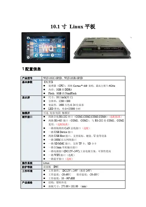
10.1寸Linux平板1配置信息产品型号WLT-101C-SP2D、WLT-101R-SP2D基本参数【配置】:●处理器(CPU):四核Cortex®-A9 架构,最高主频1.4GHz●内存:1GB的DDR3●Flash:8GB的NandFlash显示屏●尺寸:10.1 inch(英寸)●分辨率:1280×800●宽温型,1600万色或24位真彩●LED背光:寿命>25000小时触摸屏可选电容/电阻触摸屏硬件接口●四路3线RS-232串口(COM1,COM2,COM3,COM4)(选配隔离)●两路RS-485接口(COM1、COM2),与RS-232的COM1、COM2复用。
(选配隔离)●一路带隔离的CAN总线接口(选配)●一路USB Device接口●两路USB Host接口,支持鼠标、键盘、U盘等设备●一路100M以太网络接口●一路SD/MMC接口,支持TF卡,SD小卡●一路3.5mm耳机输出接口●一路电源接口(DC12V~24V),工业电源方案,可靠性更高●一路WIFI接口(选配)●一路蓝牙接口(选配)操作系统Linux防护等级前面板IP65工作环境●工作条件:DC12V ~ 24V(推荐24V)●工作温度:-20~60℃保存温度:-20~80℃●工作湿度:10~90%RH产品规格●结构:塑料外壳●面板尺寸:275.00×181.00 (mm)●机柜开孔:266.00×171 .00 (mm)应用领域●工业控制,检测设备,仪器仪表,安全监控,医疗器械,智能终端等产品嵌入式高端应用●支持CAN方便客户构建现场总线网络软件支持●推荐使用QT Creator(QT C++)开发,可灵活使用其他软件●用户可方便设定开机界面●支持屏幕旋转(0°、90°、180°、270°)2接口定义1 (12)1 CANL接口2 CANH接口3 GND4 RS-232接口COM3-RX5 RS-232接口COM3-TX6 RS-232接口COM4-RX7 RS-232接口COM4-TX 8 RS-485接口COM2-485B9 RS-485接口COM2-485A 10 GND11 RS-485接口COM1-485B 12 RS-485接口COM1-485A1 2 3 4 5 6 1USB 从机接口(USB Device) 2 USB 主机接口(USB host)3 立体音频接口4 DB9 RS-232 COM1接口5 DB9 RS-232COM2接口6 100M 以太网接口2.1RS-232接口10.1寸Linux单板电脑有四路串口,支持最高波特率115200bps。
显示器用户指南©2010Hewlett-Packard Development Company,L.P.Microsoft、Windows 和 Windows Vista 是Microsoft Corporation 在美国和/或其他国家的商标或注册商标。
HP 产品和服务的所有保修限于这些产品与服务所附带的明确保修声明。
本文的任何条款都不应视作构成保修声明的附加条款。
HP 不对本文的技术性错误、编印错误或疏漏承担任何责任。
本文档包含的所有权信息受版权保护。
未经Hewlett-Packard Company 事先书面许可,不得将本文档的任何部分影印、复制或翻译成其他语言。
第二版(2010 年 1 月)文档部件号:594300-AA2关于本指南本指南提供与安装显示器、安装驱动程序、使用屏幕显示菜单、故障排除和技术规范有关的信息。
警告!此格式的文字表示:如果不按照指示操作可能导致人身伤害,甚至死亡。
注意:此格式的文字表示:如果不按照指示操作可能致使设备损坏或信息丢失。
注:此格式的文字提供重要的附加信息。
iiiiv 关于本指南目录1 产品特性 (1)HP LCD 显示器 (1)2 安全和维护准则 (3)重要安全信息 (3)安全预防措施 (4)维护准则 (5)清洁显示器 (5)装运显示器 (5)3 安装显示器 (6)打开显示器包装 (6)安装显示器 (6)连接显示器电缆 (10)高带宽数字内容保护 (HDCP) (11)连接音频电缆 (12)连接电源线 (13)调整显示器的倾斜角度 (13)调整扭转角度 (14)键盘存放 (15)4 操作显示器 (16)CD 软件和实用程序 (16)安装驱动程序 (16)使用自动调整功能 (17)前面板控制按钮 (18)使用屏幕显示 (OSD) (19)选择视频输入接口 (23)识别显示器状况 (23)调整屏幕质量 (24)省电功能 (24)v附录 A 故障排除 (26)解决常见问题 (26)从 获取支持 (27)准备致电技术支持 (27)查找额定值标签 (28)附录 B 技术规格 (29)HP LCD 显示器 (29)预设视频模式 (33)LCD 显示器质量和像素策略 (35)附录 C 机构规定注意事项 (36)(美国)联邦通信委员会注意事项 (36)修改 (36)电缆 (36)标有 FCC 徽标的产品的一致性声明(仅适用于美国) (36)适用于加拿大的注意事项 (37)Avis Canadien (37)欧盟规程通告 (37)德国人机工程学通告 (38)适用于日本的注意事项 (38)适用于韩国的注意事项 (38)电源线配件要求 (38)适用于日本的电源线要求 (38)产品环境注意事项 (39)废弃物品的处理 (39)日常处理废旧器件的注意事项(适用于欧盟) (39)化学物质 (39)HP 回收办法 (39)有害物质的限制 (RoHS) (39)土耳其 EEE 法规 (40)vi1产品特性HP LCD 显示器HP LCD(液晶显示)显示器采用具备有源矩阵和下列特性的薄膜晶体管 (TFT) 屏幕:●大尺寸屏幕●最大图像分辨率:◦1910m:1366x768@60 赫兹◦2010f:1600x900@60 赫兹◦2010i:1600x900@60 赫兹◦2010m1600x900@60 赫兹◦2210i:1920x1080@60 赫兹◦2210m:1920x1080@60 赫兹◦2310i:1920x1080@60 赫兹◦2310m:1920x1080@60 赫兹◦2510i:1920x1080@60 赫兹◦2710m:1920x1080@60 赫兹◦且支持较低分辨率的全屏显示●VGA 模拟信号●DVI 数字信号●高清晰度多媒体接口 (HDMI)(适用于部分型号)●反应迅捷,玩核心游戏和图形制作时可获得更佳效果●视角宽广,无论是坐着、站着还是从显示器的两侧,均易于观看●动态对比度,提供更深的黑度和更亮的白度以实现出众的色差效果,令玩游戏和观看电影更具特色●倾斜度调整●扭转角度调整HP LCD 显示器1●可拆卸式的底座和符合视频电子标准协会 (Video Electronics Standards Association,VESA) 标准的安装孔,便于进行灵活的安装(包括墙上安装)●安全锁定插槽,用于连接安全锁定电缆(需要单独购买安全电缆)●即插即用功能(如果您的计算机系统支持此功能)●屏幕显示 (OSD) 可调,便于设置和优化屏幕(可选择英文、简体中文、繁体中文、法文、德文、意大利文、西班牙文、荷兰文、日文或巴西葡萄牙文)●内置立体声低音炮扬声器●键盘存放装置●节能装置,有助于减少能源消耗●“快速查看”设置显示●DVI 和 HDMI 输入具有 HDCP(高带宽数字内容保护)(适用于部分型号)●软件和实用程序 CD,其中包含以下内容:◦驱动程序◦自动调整软件◦相关文档2第 1 章 产品特性2安全和维护准则重要安全信息本显示器已附带电源线。
jw85006规格书1. 引言本规格书旨在详细描述jw85006产品的技术规格和功能要求。
该产品是一种先进的电子设备,具有广泛的应用领域。
本规格书旨在为设计师、制造商和用户提供清晰的产品说明,并确保产品在设计、制造和使用过程中能够满足各种技术要求和性能指标。
2. 产品描述jw85006是一款基于先进技术开发的电子设备,具有以下主要特点和功能:2.1 技术特点•高性能处理器:采用先进的处理器芯片,具有强大的计算能力和高效的数据处理能力。
•多功能操作系统:支持多种操作系统,如Windows、Linux等,提供灵活的软件运行环境。
•大容量存储器:内置大容量存储器,可存储大量数据和应用程序。
•高清显示屏:配备高分辨率的显示屏,显示效果清晰逼真。
•多种接口:支持多种接口,如USB、HDMI等,方便与外部设备进行连接和数据传输。
2.2 功能要求•数据处理:能够高效地进行数据处理和计算,满足各种复杂的数据处理需求。
•多媒体功能:支持多媒体数据的播放和编辑,具有良好的音视频效果。
•网络通信:具备网络通信功能,支持有线和无线网络连接,能够实现远程数据传输和远程控制。
•安全性能:具备良好的安全性能,能够保护用户数据的安全和隐私。
•系统稳定性:具有稳定可靠的系统运行,能够长时间稳定工作而不出现系统崩溃和死机等问题。
3. 技术规格3.1 外观设计•尺寸:长 x 宽 x 高,约为X cm x Y cm x Z cm•材质:采用高强度塑料外壳,具有良好的抗冲击性和防尘防水性能。
•颜色:可供选择的颜色有黑色、白色、银色等,也可根据客户需求定制。
•按键布局:合理布局的按键,易于操作和控制。
3.2 硬件配置•处理器:型号X,主频Y GHz,核心数Z•内存:容量X GB,类型Y•存储器:容量X GB,类型Y•显示屏:尺寸X 英寸,分辨率Y 像素•电池:容量X mAh,工作时间约为Y 小时3.3 软件功能•操作系统:支持的操作系统有A、B、C等,提供丰富的软件资源和应用程序。
10寸产品规格书1. 产品概述本文档为10寸产品规格书,旨在详细介绍该产品的规格和特点。
该产品是一款10寸尺寸的设备,具有多种功能和特性,适用于各种应用场景。
2. 外观和尺寸•尺寸: 10寸 x 7寸 x 0.5寸•材料: 高质量塑料外壳•颜色: 亮黑色•按钮: 电源按钮,音量控制按钮,功能键3. 显示屏•类型: TFT液晶显示屏•尺寸: 10寸•分辨率: 1920 x 1200像素•背光: LED背光•触控: 支持多点触控•显示比例: 16:104. 硬件规格•处理器: 四核 Cortex A53 1.5GHz•内存: 4GB DDR3•存储: 64GB 闪存•扩展存储: microSD卡插槽,最大支持128GB •电池容量: 5000mAh•无线连接: Wi-Fi 802.11ac,蓝牙4.25. 操作系统•操作系统: Android 10•支持多语言界面•支持应用商店下载和安装6. 摄像头•后置摄像头: 800万像素•前置摄像头: 500万像素•支持拍照和录像功能7. 输入输出接口•USB接口: Micro USB•音频接口: 3.5mm耳机插孔•扩展接口: microSD卡插槽8. 通信功能•蜂窝网络: 支持2G/3G/4G网络•GPS导航: 支持全球定位系统导航•蓝牙: 支持蓝牙4.2•无线网络: Wi-Fi 802.11ac 9. 其他特性•加速传感器•重力传感器•音频支持: 支持常见音频格式•视频支持: 支持常见视频格式10. 包装清单•10寸产品•充电器•USB数据线•用户手册以上是10寸产品规格书的详细内容,希望能对您了解该产品提供帮助。
如有其他问题,请随时与我们联系。
手机显示屏技术规范1.目的:规范本公司手机显示屏设计及检测。
2.适用范围:适用于研发设计开发、样品认证测试及品质来料检验。
3.技术要求使用环境:工作温度:-20℃~55℃储存稳定:-30℃~65℃相对湿度:≤93%大气压力:70~106kpa技术参数显示类型:TFT、CSTN、OLED等显示模式:透射、半透半反射等TFT:视角:一般3:00 6:00 12:00 全视角点阵:QQVGA,QCIF,QVGA,WQVGA,HVGA,VGA等尺寸规格(英寸):1.0,1.1,1.5,1.8,2.0,2.2,2.4,2.6,2.8,3.0 ,3.2等工作电压:一般2.8VI/O电压:1.8V或2.8V,需和工作电压分开响应时间:响应时间的定义::上升时间,透过率从90%(白色)变化到10%(黑色)的时间;TRT:下降时间,透过率从10%(黑色)变化到90%(白色)的时间;FSTN 响应时间一般在300-400ms;(低温下的相应时间及显示效果,需给出一个标准)CSTN响应时间一般在200-300ms;(低温下的相应时间及显示效果,需给出一个标准)手机小尺寸TFT 响应时间一般在30-50ms.主要影响因素是三者由上到下盒厚递减,液晶分子扭转力递减;且液晶电压递增,加电电场递增。
数据接口:CPU或RGB显示效果判断目测颜色较鲜艳1、GAMMA测试测试方法:(测试设备)⑴将64阶灰度图片拷入手机,并显示图片、使用仪器测试结果、记录数据。
GAMMA曲线比较平滑,且DIFF-GAMMA曲线的差异在0-20灰阶小于5,在20—63灰阶小于13;⑵在20-50灰阶之间不可以有交点;⑶ CSTN暂不做要求。
判定标准:DIFF-GAMMA曲线的量化,用测的曲线减去2.2标准曲线的差值绘成曲线图,将GAMMA 曲线改为:0为黑色,63为白色。
2、RGB GAMMA测试测试方法:⑴ RGB GAMMA曲线变化平缓且蓝色曲线在曲定书线上方,RGB差异曲线的差异小于20;⑵ CSTN暂不做要求。
CUSTOMER APPROVAL SHEETCompany NameMODEL A104SN03 V1CUSTOMER APPROVED Title : Name :□ APPROVAL FOR SPECIFICATIONS ONLY (Spec. Ver. )□ APPROVAL FOR SPECIFICATIONS AND ES SAMPLE (Spec. Ver. )□ APPROVAL FOR SPECIFICATIONS AND CS SAMPLE (Spec. Ver. )□ CUSTOMER REMARK :AUO PM :P/N :Comment :1 Li-Hsin Rd. 2. Science-Based Industrial ParkHsinchu 300, Taiwan, R.O.C.Tel: +886-3-500-8899Doc. version : 0.7Total pages : 34Date : 2009/04/27Product Specification10.4" COLOR TFT-LCD MODULE Model Name:A104SN03 V1Planned Lifetime: From 2008/Dec To 2010/Dec Phase-out Control:From 2010/Jul To 2010/Dec EOL Schedule: 2010/Decary Specification< >Final SpecificationNote: The content of this specification is subject to change.© 2009 AU Optronics All Rights Reserved, Do Not Copy.Page: 1/34Record of RevisionVersion Revise Date Page Content0.0 2008/10/29All First Draft0.1 2008/11/1224 Update Response time29 Update drawing0.2 2009/01/07 4 Update drawing17 Update Register Table18 Delete R1 setting0.3 2009/1/16 4 Update drawing10 Delete extra Electrical DC Characteristics32 Add Application Circuit0.4 2009/02/048 Delete extra note0.5 2009/03/1512 Add VCOMin22 Delete Power on R133 Update Application Circuit0.6 2009/03/3125 Update Contrast ratio0.7 2009/4/27 19 Update Register Table & Register DescriptionPage: 2/34ContentsA.General Information (3)B.Outline Dimension (4)1.TFT-LCD Module (4)C.Electrical Specifications (6)1. TFT LCD Panel Pin Assignment (6)2. Backlight Pin Assignment (9)3. Absolute Maximum Ratings (9)3. Electrical DC Characteristics (10)4. Electrical AC Characteristics (14)5. Serial Interface Characteristics (17)6. Power On/Off Characteristics (22)D.Optical Specification (25)E.Reliability Test Items (28)F.Packing and Marking (31)1. Packing Form (31)2. Module/Panel Label Information (32)3. Carton Label Information (32)G.Application Note (33)Application Circuit (33)H.Precautions (34)Page:3/34A. General InformationThis product is for portable DVD and digital photo frame application.NO. ItemUnit SpecificationRemark1 Screen Sizeinch 10.4(Diagonal)2 Display Resolutiondot800RGB(W)x600(H)3 Overall Dimensionmm 228.4(W)x175.4(H)x6.2(D)Note 1 4 Active Area mm211.2(W)x158.4(H)5 Pixel Pitchmm 0.264(W)x0.264(H) 6 Color Configuration-- R. G. B. Stripe Note 27 Color Depth -- 16.7M ColorsNote 3 8 NTSC Ratio% 509Display Mode-- Normally White 10 Panel surface Treatment --Anti-Glare, 3H11 Weightg400±2012 Panel Power ConsumptionW 0.43Note 4 13 Backlight Power Consumption W 2.97 14 Viewing direction6 o’clock (gray inversion)Note 1: Not include blacklight cable and FPC. Refer next page to get further information. Note 2: Below figure shows dot stripe arrangement.Note 3: The full color display depends on 24-bit data signal (pin 4~27). Note 4: Please refer to Electrical Characteristics chapter.( 1…………...……………..600 )V e r s i o n :0.7P a g e : 4/34I G H T S S T R I C T L Y R E S E R V E D . A N Y P O R T I O N O F T H I S P A P E R S H A L L N O T B E R E P R O D U C E D , C O P I E D , O R T R A N S F O R M E D T O A N Y O T H E R F O W I T H O U T P E R M I S S I O N F R O M A U O P T R O N I C S C O R P .O u t l i n e D i m e n s i o n1. T F T -L C D M o d u l eV e r s i o n :0.7P a g e : 5/34I G H T S S T R I C T L Y R E S E R V E D . A N Y P O R T I O N O F T H I S P A P E R S H A L L N O T B E R E P R O D U C E D , C O P I E D , O R T R A N S F O R M E D T O A N Y O T H E R F O W I T H O U T P E R M I S S I O N F R O M A U O P T R O N I C S C O R P .Page: 6/34 C. Electrical Specifications1. TFT LCD Panel Pin AssignmentRecommended connector : HRS FH28-60S-0.5SHPin no Symbol I/O Description Remark1 AGND P Ground for analog circuit2 AVDD P Analog power supply voltage3 VDDIO P Digital interface supply voltage4 R0 I Red data input (LSB)5 R1 I Red data input6 R2 I Red data input7 R3 I Red data input8 R4 I Red data input9 R5 I Red data input10 R6 I Red data input11 R7 I Red data input (MSB)12 G0 I Green data input (LSB)13 G1 I Green data input14 G2 I Green data input15 G3 I Green data input16 G4 I Green data input17 G5 I Green data input18 G6 I Green data input19 G7 I Green data input (MSB)20 B0 I Blue data input (LSB)21 B1 I Blue data input22 B2 I Blue data input23 B3 I Blue data input24 B4 I Blue data input25 B5 I Blue data input26 B6 I Blue data input27 B7 I Blue data input (MSB)28 DCLK I Data clock input29 DE I Data enable signal30 HSYNC I Horizontal sync input. (Negative polarity)31 VSYNC I Vertical sync input. (Negative polarity)32 SCL I Serial communication clock input33 SDA I Serial communication data input34 CSB I Serial communication chip selectPage:7/3435NC-For test, do not connect (Please leave it open)36 VDDIO P Digital interface supply voltage 37 NC - For test, do not connect (Please leave it open)38 GND P Ground for digital circuit 39 AGND P Ground for analog circuit 40 AVDDP Analog power supply voltage41VCOMin IFor external VCOM DC input 42 DITH IDithering setting DITH = "L" 6bit resolution(LSB last 2 bits of input data turncated)DITH = "H" 8bit resolution(Default setting)43 NC- For test, do not connect (Please leave it open) 44 VCOM O connect a capacitor 45 V10 I Gamma correction voltage reference 46 V9 I Gamma correction voltage reference 47 V8 I Gamma correction voltage reference 48 V7 I Gamma correction voltage reference 49 V6 I Gamma correction voltage reference 50 V5 I Gamma correction voltage reference 51 V4 I Gamma correction voltage reference 52 V3 I Gamma correction voltage reference 53 V2 I Gamma correction voltage reference 54 V1IGamma correction voltage reference55 NC - For test, do not connect (Please leave it open)56 VGH P Positive power for TFT57 VDDIO P Digital interface supply voltage 58 VGL P Negative power supply for Gate driver.59 GND P Ground for digital circuit 60 NC-For test, do not connect (Please leave it open)I: Input; P: PowerPage: 8/34.Page:9/342. Backlight Pin AssignmentRecommended connector : JOIN TEK JT1025-1021Pin no Symbol I/O Description Remark1 VLED+ P Backlight LED anode2VLED-PBacklight LED cathode3. Absolute Maximum RatingsItemSymbol Conditio Min. Max. Unit Remark VDDIO GND=0 -0.5 5 V Digital Power Supply AVDDAGND=0 -0.5 15 VAnalog power supplyVGH -0.3 42 V Gate driver supply voltage VGL GND=0-20 0.3 V Gate driver supply voltage Power voltageVGH -VGL- 40V Gate driver supply voltageV I -0.3 VDDIO+0.3 VNote 1 Input signal voltageVCOMin 0 5 VVCOM DC VoltageOperating Topa -10 60 StorageTstg-2070Note 1: Functional operation should be restricted under ambient temperature.Note 2: Maximum ratings are those values beyond which damages to the device may occur. Functional operation should be restricted to the limits in the Electrical Characteristics chapter.Page: 10/343. Electrical DC Characteristicsa. Typical Operation Condition (AGND =GND = 0V)Item Symbol Min. Typ.Max. Unit RemarkVDDIO 3.0 3.3 3.6 V Digital Power SupplyAVDD 10.5 11 11.5 V Analog Power Supply Power VoltageVGH 14 15 16 V Positive power supply for gatedriverVGL -7.5 -7 -6.5 V Negative power supply forgate driver InputH Level VIH 0.7xVDDIO-- VDDIO VSignal Voltage L Level VIL GND -- 0.3xVDDIO VGamma referenceV1 ~ V5AVDD/2 - AVDD – 1V Note 1 voltage V6 ~ V10 1 - AVDD/2 VVCOMin V CDC 3.75 3.95 4.15 V Note 2 Note 1: Gamma suggested circuit is as followsPage: 11/34 Pin Voltage(V)AVDD 11V1 10V2 8.5V3 8V4 7.57V5 6.7V6 4.3V7 3.43V8 3V9 2.5V10 1Page: 12/34 Note2: Based on recommended Gamma 2.2 voltage.Page: 13/34b. Current Consumption (AGND=GND=0V)Parameter Symbol Condition Min. Typ. Max. Unit Remark Input current for VDDIO IVDDIO VDDIO = 3.3V 10 20 m A Note 1, 2 Input current for AVDD IAVDD AVDD = 11V 24 30 mA Note 1, 2 Input current for VGH IVGH VGH = 15V -- 0.4 0.6 mA Note 1, 2 Input current for VGL IVGL VGL = -7V -0.6 -0.4 -- mA Note 1, 2 Note 1:Test Condition is under typical Eletrical DC and AC characteristics.Note 2: Test pattern is the following picture.c. Backlight Driving ConditionsThe backlight (LED module, Note 1) is suggested to drive by constant current with typical value.Parameter Symbol Min. Typ. Max. Unit Remark LED light bar Current I L-- 300 -- mAPower Consumption P -- 3 3.21 W Note 1 LED Life Time L L10,000 -- -- Hr Note 2, 3 Note 1: The LED driving condition is defined for LED module (36 LED). The Voltage range will be 8.8V to 10.7V based on suggested driving current set as 300mA.Note 2: Define “LED Lifetime”: brightness is decreased to 50% of the initial value. LED Lifetime is restricted under normal condition, ambient temperature = 25℃and LED lightbar current =300mA.Note 3: If it uses larger LED lightbar current more than 300mA, it maybe decreases the LED lifetime.Page: 14/344. Electrical AC Characteristicsa. Signal AC CharacteristicsParameter Symbol Min. Typ. Max. Unit Remark DCLK duty cycle -- 40 50 60 % t cw / t DCLK x100% VSYNC setup time t vst0 -- -- nsVSYNC hold time t vhd 2 -- -- nsHSYNC setup time t hst 5 -- -- nsHSYNC hold time t hhd10 -- -- nsData setup time t dst 5 -- -- nsData hold time t dhd10 -- -- nsData enable set-up time t est 4 -- -- nsData enable hold time t ehd 2 -- -- nsPage:15/34b. Input TimingHS R[7:0]G[7:0]B[7:0]DCLKHorizontal input timing. (HV mode)DCLK DER[7:0]G[7:0]B[7:0]Horizontal TimingParameter Symbol Min. Typ. Max. Unit. RemarkDCLK frequency F DCLK 25 40 45 MHz DCLK periodT DCLK 22 25 40 ns Hsync period (= T HD + T HBL )T H 1026 1056 1183 DCLK Active AreaT HD - 800 - DCLK Horizontal blanking (= T HF + T HE )T HBL 226 256 383 DCLK Hsync front porchT HF 10 40 167 DCLK Delay from Hsync to 1st data input(= T HW + T HB )T HE216DCLKPage: 16/34 Hsync pulse width T HW 1 128 136 DCLKHsync back porch T HB80 88 215 DCLKHorizontal input timing (HV mode)Horizontal input timing (DE mode)Vertical TimingParameter Symbol Min. Typ. Max. Unit. Remark Vsync period (= T VD + T VBL) T V- 628 635 ThActive lines T VD- 600 - Th Vertical blanking (= T VF + T VE) T VBL- 28 35 ThVsync front porch T VF- 1 8 ThGD start pulse delay T VE- 27 - ThVsync pulse width T VW 1 3 16 ThHsync/Vsync phase shift T VPD 2 320 - DCLKPage: 17/34Vertical timing (HV mode)Vertical timing (DE mode)5. Serial Interface Characteristicsa. Serial Control Interface AC CharacteristicParameter Symbol Min. Typ. Max. Unit. Remark Serial data setup time T IST120 - - nsSerial data hold time T IHD120 - - nsCSB setup time T CST120 - - nsCSB hold time T CHD120 - - nsSerial clock high/low T SSW120 - - nsSerial clock T SCK320 - - nsDelay from CSB to VSYNC T CV 1 - - usChip select distinguish T CD 1 - - usSerial data output delay T ID- - 60 ns CL=20pFPage: 18/34b Serial Interface TimingThere is a total of 6 registers each containing several parameters. For a detailed description of the parameters refer to register table. The serial register has read/write function. D[15:12] are the register address, D[11] defines the read or write mode and D[10:0] are the data.Serial Interface Write sequence1. At power-on, the default values specified for each parameter are taken.2. If less than 16-bit data are read during the CS low time period, the data is cancelled.a. The write operation is cancelled.3. All items are set at the falling edge of the vertical sync, except R0[1:0].4. When GRB is activated through the serial interface, all registers are cleared, except the GRB value.5. The register setting values are valid when VCC already goes to high and after VSYNC starts.6. It is suggested that VSYNC, HSYNC, DCLK always exists in the same time. But if HSYNC, DCLK stops,only VSYNC operating, the register setting is still valid.7. If the chip goes to standby mode, the register value will still keep. MCU can wake up the chip only bychanging standby mode value from low to high.8. The register setting values are rewritten by the influence of static electricity, a noise, etc. to unsuitable value,incorrect operating may occur. It is suggested that the SPI interface will setup as frequently as possible.Page:19/34c. Register Table (Default Value)RegADDRESSR/WDATA No. D15 D14 D13 D12 D11 D10 D9D8D7D6 D5 D4 D3 D2 D1D0R0 0 0 0 0 0 (01)(01) (1)(0)(1) (1)(0)GRB (1)STB (1)R2 0 0 1 0 0 × × × HDL(80h)R3 0 0 1 1 0 × × (0) (0) (0) (0) (0) VDL(1000)R4 0 1 0 0 0 × × (1)(0) (0)(0) (1) (1111)R6 011×(0)EnGB12 (1)EnGB11 (1)EnGB10 (1)(0)(0)EnGB5 (1)EnGB4 (1)EnGB3 (1)(0)X: Reserved. Please set to “0”.<Note>:Sending serial commands periodically is recommended to improve ESD protection ability.d. Register Descriptiona. R0 setting AddressBitDescriptionDefault 0000 [10..0] Bits 10-9 AUO Internal Use 01 Bits7-8AUO Internal Use 01 Bit6 (DITH) Dithering function. 1 Bit5 AUO Internal Use 0 Bit4 AUO Internal Use 1 Bit3 AUO Internal Use. 1 Bit2 AUO Internal Use 0 Bit1 (GRB) Global reset.1Bit0 (STB) Standby mode setting.1Bit6 DITH function0 DITH off.1DITH on. (default)Bit1GRB function0 The controller is reset. Reset all registers to default value. 1Normal operation. (default)Bit0STB function0 T-CON and source driver are off. All outputs are set to GND.1Normal operation. (default)Address Bit Description Default 0010 [7..0] Bit7-0(HDL) Horizontal start pulse adjustment function80H Bit7-0 HDL function00h T HE = T HEtyp - 128 CLK period.80h T HE = T HEtyp. (default)FFh T HE = T HEtyp + 127 CLK period.c. R3 settingAddress Bit Description Default 0011[8..0]Bit8 AUO Internal Use0Bit7 AUO Internal Use0Bit6 AUO Internal Use 0Bit5 AUO Internal Use 0Bit4 AUO Internal Use 0Bit3-0(VDL) Vertical start pulse adjustment function 1000Bit3-0 VDL function0000 T VE = T VEtyp – 8 Hs period.0001 T VE = T VEtyp – 7 Hs period.0010 T VE = T VEtyp – 6 Hs period.0011 T VE = T VEtyp – 5 Hs period.0100 T VE = T VEtyp – 4 Hs period.0101 T VE = T VEtyp – 3 Hs period.0110 T VE = T VEtyp – 2 Hs period.0111 T VE = T VEtyp – 1 Hs period.1000 T VE = T VEtyp. (default)1001 T VE = T VEtyp – 1 Hs period.1010 T VE = T VEtyp – 2 Hs period.1011 T VE = T VEtyp – 3 Hs period.1100 T VE = T VEtyp – 4 Hs period.1101 T VE = T VEtyp – 5 Hs period.1110 T VE = T VEtyp – 6 Hs period.1111 T VE = T VEtyp – 7 Hs period.Address Bit Description Default 0110 [9..0] Bits9 AUO Internal Use 0Bits8(EnGB12)Gamma buffer Enable for V9 1Bits7(EnGB11)Gamma buffer Enable for V8 1Bits6(EnGB10)Gamma buffer Enable for V7 1Bits5 AUO Internal Use 0Bits4 AUO Internal Use 0Bits3(EnGB5) Gamma buffer Enable for V4 1Bits2(EnGB4) Gamma buffer Enable for V3 1Bits1(EnGB3) Gamma buffer Enable for V2 1Bits0 AUO Internal Use 0 Bitx EnGBx function0 Gamma buffer for VX is disabled (High Z).1 Gamma buffer is enabled. VX must be connected externally.Page: 22/346. Power On/Off Characteristicsa. Recommended Power On Register SettingADDRESS R/W DATARegNo.D15D14D13D12D11D10 D9 D8 D7 D6 D5 D4 D3 D2 D1 D0 R00000010 01 1 0 1 0 0 1 1 R2001000 0 0 80hR3001100 0 0 0 0 0 0 1000R4010000 0 1 1 00 1 1111R6011000 0 1 1 1 0 0 1 1 1 0Note : Start to provide SPI commend at least after 2 frame.1. Send R15 : 000h(Normal register bank) at first.2. Wait at least after more than one frame, send R0 : 4D1h(Global Reset)3. After send Global Reset, start to send R0 to R6 recommend register value.V e r s i o n :0.7P a g e : 23/34G H T S S T R I C T L Y R E S E R V E D . A N Y P O R T I O N O F T H I S P A P E R S H A L L N O T B E R E P R O D U C E D , C O P I E D , O R T R A N S F O R M E D T O A N Y O T H E R F O R M S W I T H O U T P E R M I S S I O N F R O M A U O P T R O N I C S C O R P .R e c o m m e n d e d P o w e r O n S e q u e n c eV e r s i o n :0.7P a g e : 24/34G H T S S T R I C T L Y R E S E R V E D . A N Y P O R T I O N O F T H I S P A P E R S H A L L N O T B E R E P R O D U C E D , C O P I E D , O R T R A N S F O R M E D T O A N Y O T H E R F O R M S W I T H O U T P E R M I S S I O N F R O M A U O P T R O N I C S C O R P .P o w e r O f f S e q u e n c ePage:25/34D. Optical SpecificationAll optical specification is measured under typical condition (Note 1, 2)Item Symbol Condition Min. Typ. Max. Unit Remark Response TimeRise FallTr Tfθ=0°-- --307 33ms ms Note 3 Contrast ratioCR At optimizedviewing angle 400 500 -- Note 4TopBottom Left Viewing AngleRight4050 65 6550 60 75 75 -- -- -- -- deg. Note 5BrightnessY Lθ=0° 250300 --cd/m 2 Note 6X θ=0° 0.28 0.33 0.38 White Y θ=0° 0.30 0.35 0.40 X θ=0° 0.550 0.600 0.650 RedY θ=0° 0.324 0.374 0.424 X θ=0° 0.306 0.356 0.406 Green Y θ=0° 0.531 0.581 0.631 X θ=0° 0.094 0.144 0.194 ChromaticityBlueY θ=0° 0.043 0.093 0.143 UniformityΔY L%7580--Note 7Note 1: Ambient temperature =25℃, and LED lightbar current I L = 300mA. To be measured in the dark room.Note 2: To be measured on the center area of panel with a viewing cone of 1° by Topcon luminance meterBM-5A, after 15 minutes operation.Page:26/34The output signals of photo detector are measured when the input signals are changed from “black” to “white”(falling time) and from “white” to “black”(rising time), respectively.The response time is defined as the time interval between the 10% and 90% of amplitudes. Refer to figure as below.Note 4.Definition of contrast ratio:Contrast ratio is calculated with the following formula.statusBlack"" at is LCD when output detector Photo statusWhite"" at is LCD when output detector Photo (CR) ratio Contrast =Note 5. Definition of viewing angle, θ, Refer to figure as below.Note 6. Measured at the center area of the panel when all the input terminals of LCD panel are electrically opened.Note 7: Luminance Uniformity of these 9 points is defined as below:Page: 27/34Page: 28/34 E. Reliability Test ItemsNo.Test items Conditions Remark1 High Temperature Storage 240Hrs2 Low Temperature Storage Ta= -2240Hrs3 High Ttemperature Operation Tp= 240Hrs4 Low Temperature Operation Ta=-1240Hrs5 High Temperature & High Humidity Tp240Hrs Operation6 Heat Shock -Non-operation7 Electrostatic Discharge Contact = ± 4 kV, class BAir = ± 8 kV, class B Note 58 Image Sticking 254hrs Note 6Frequency range : 10~55HzStoke : 1.5mmSweep : 10 ~ 55 ~ 10Hz2 hours for each direction of X,Y,Z 9 Vibration(6 hours for total)Non-operation JIS C7021, A-10 condition A : 15 minutes10Mechanical Shock 100G . 6ms, ±X,±Y,±Z3 times for each direction Non-operation JIS C7021,A-7 condition C11Vibration (With Carton)Random vibration:0.015G2/Hz from 5~200Hz–6dB/Octave from 200~500HzIEC 68-3412Drop (With Carton) Height: 60cm1 corner, 3 edges, 6 surfaces13Pressure 5kg, 5sec Note 7 Note 1: Ta: Ambient Temperature. Tp: Panel Surface TemperatureNote 2: In the standard conditions, there is not display function NG issue occurred. All the cosmetic specification is judged before the reliability stress.Note 3: All the cosmetic specification is judged before the reliability stress.Note5 : All test techniques follow IEC6100-4-2 standard.Page:29/34Contact Discharge :330Ω, 150pF, 1sec, 8 point, 10times/pointAir Discharge :330Ω, 150pF, 1sec, 8 point, 10times/point Then judge with 50% gray level, the mura is less than JND 2.5Note 7: The panel is tested as figure. The jig isψ10 mm made by Cu with rubber and the loadingspeed is 3mm/min on position A~E. After the condition, no glass crack will be found and panelfunction check is OK.( no guarantee LC mura 、LC bubble)Page: 30/34Page: 31/34 F. Packing and Marking1. Packing FormPage: 32/342. Module/Panel Label InformationThe module/panel (collectively called as the “Product”) will be attached with a label of Shipping Number which represents the identification of the Product at a specific location. Refer to the Product outline drawing for detailed location and size of the label. The label is composed of a 22-digit serial number and printed with code 39/128 with the following definition:Example:501M06ZL06123456781Z05:Product Manufacturing Week Code: WK50Product Version: Version 1Product Manufactuing Factory: M063. Carton Label InformationThe packing carton will be attached with a carton label where packing Q’ty, AUO Model Name, AUO Part Number, Customer Part Number (Optional) and a series of Carton Number in 13 or 14 digits are printed. The Carton Number is apparing in the following format:Refer to the drawing of packing format for the location and size of the carton label.V e r s i o n :0.7P a g e : 33/34R I G H T S S T R I C T L Y R E S E R V E D . A N Y P O R T I O N O F T H I S P A P E R S H A L L N O T B E R E P R O D U C E D , C O P I E D , O R T R A N S F O R M E D T O A N Y O T H E R F O R M S W I T H O U T P E R M I S S I O N F R O M A U O P T R O N I C S C O R P .A p p l i c a t i o n N o t ep p l i c a t i o n C i r c u i tVersion: 0.7Page: 34/34H. Precautions1. Do not twist or bend the module and prevent the unsuitable external force for display module duringassembly.2. Adopt measures for good heat radiation. Be sure to use the module with in the specified temperature.3. Avoid dust or oil mist during assembly.4. Follow the correct power sequence while operating. Do not apply the invalid signal, otherwise, it willcause improper shut down and damage the module.5. Less EMI: it will be more safety and less noise.6. Please operate module in suitable temperature. The response time & brightness will drift by differenttemperature.7. Avoid to display the fixed pattern (exclude the white pattern) in a long period, otherwise, it will causeimage sticking.8. Be sure to turn off the power when connecting or disconnecting the circuit.9. Polarizer scratches easily, please handle it carefully.10. Display surface never likes dirt or stains.11. A dewdrop may lead to destruction. Please wipe off any moisture before using module.12. Sudden temperature changes cause condensation, and it will cause polarizer damaged.13. High temperature and humidity may degrade performance. Please do not expose the module to thedirect sunlight and so on.14. Acetic acid or chlorine compounds are not friends with TFT display module.15. Static electricity will damage the module, please do not touch the module without any groundeddevice.16. Do not disassemble and reassemble the module by self.17. Be careful do not touch the rear side directly.18. No strong vibration or shock. It will cause module broken.19. Storage the modules in suitable environment with regular packing.20. Be careful of injury from a broken display module.21. Please avoid the pressure adding to the surface (front or rear side) of modules, because it will causethe display non-uniformity or other function issue.22. Please use SSCG(Spread Spectrum Clock Generator) at system for EMI reduction.。
DP10L、S系列电梯液晶显示器说明书一、产品规格:1、型号说明:代码说明L:大显示板 190.95(mm)X 109.50(mm)X43(mm)aS:小显示板 164.70(mm)X 109.50(mm)(mm)bA:大显示屏(可视区域:132.0(W)mm X 76.0(H)mm)B:小显示屏(可视区域:114.0(W)mm X 64.0 (H)mm )1:蓝膜,蓝底白字2:红紫膜,红紫色底米黄色字c3:黑白膜,白底黑字(半透)4:黑白膜,黑底白字5:黑白膜,白底黑字(全透)2、显示信息:时钟显示,方向、检测、直驶、超载、满载、停止、独立运行;标准作业时显示楼层为-9~99。
3、显示屏显示信息字体大小(宽X高):⑴、楼层显示字体:大显示屏(横显示):24.00(mm)X 46.00(mm)(竖显示):24.00(mm)X 44.00(mm)小显示屏(横显示):21.12(mm)X 40.48(mm)(竖显示):21.12(mm)X 38.72(mm)⑵、箭头大小:大显示屏(横显示):36.00(mm)X 30.00(mm)(竖显示):32.00(mm)X 35.00(mm)小显示屏(横显示):31.68(mm)X 26.40(mm)(竖显示):28.16(mm)X 30.80(mm)⑶、电梯信息的字体:大显示屏(横显示):24.00(mm)X 10.00(mm)(竖显示):12.00(mm)X 20.00(mm)小显示屏(横显示):21.12(mm)X 8.8(mm)(竖显示):10.56(mm)X 17.6(mm)⑷、检测显示大小:大显示屏(横显示):48.00(mm)X 52.5(mm)(竖显示):48.00(mm)X 48.00(mm)小显示屏(横显示):42.24(mm)X 46.20(mm)(竖显示):42.24(mm)X 42.24(mm)⑸、时间显示大小:大显示屏:3.00(mm)X 4.00(mm)二、基本参数:1、工作电压:DC12V~24V2、工作电流:<300mA(DC24V)3、工作环境温度:0~50摄氏度4、工作环境温度:10%~90%5、信号触发:信号电压:DC24V,电平触发。
液晶显示屏接口定义液晶屏常见接口样式与区别方法从屏的接口样式简单区分屏接口类型的方法很多初学者对于如何区分屏的接口类型很是头疼,是LVDS屏,TTL屏还是RSDS屏?总是很难搞清出。
如何快速识别出液晶屏的接口类型则需要一些经验的,下面从屏的屏线接口的样式来对接口类型做出分类的介绍,帮助大家快速识别屏的接口类型。
以下方法是个人认识,不足之处请大家谅解。
(1)TTL屏接口样式:D6T(单6位TTL):31扣针,41扣针。
对应屏的尺寸主要为笔记本液晶屏(8寸,10寸,11寸,12寸),还有部分台式机屏15寸为41扣针接口。
S6T(双6位TTL):30+45针软排线,60扣针,70扣针,80扣针。
主要为台式机的14寸,15寸液晶屏。
D8T(单8位TTL):很少见S8T(双8位TTL):有,很少见80扣针(14寸,15寸)2)LVDS屏接口样式:D6L(单6位LVDS):14插针,20插针,14片插,30片插(屏显基板100欧姆电阻的数量为4个)主要为笔记本液晶屏(12寸,13寸,14寸,15寸)D8L(单8位LVDS):20插针(5个100欧姆)(15寸)S6L(双6位LVDS):20插针,30插针,30片插(8个100欧姆)(14寸,15寸,17寸)S8L(双8位LVDS):30插针,30片插(10个100欧姆电阻)(17寸,18寸,19寸,20寸,21寸)3)RSDS屏接口样式:50排线,双40排线,30+50排线。
主要为台式机(15寸,17寸)液晶屏。
这是笔记本用的20针lvds接口这是普通用的液晶显示器用点屏线:左边接驱动板,右边接液晶屏(20针与30针lvds接口相似)这里面都是lvds接口:有30针、20针的这些是41扣针接口(双排)这是60扣针接口(80扣针接口与这个相似)本贴来自天极网群乐社区--/group/review-9288206.html液晶屏接口定义(2008-01-18 18:09:43)孤影清风的BLOG20PIN单6定义:3.3V 3.3V1:电源2:电源3:地 4:地 5:R0- 6:R0+ 7:地 8:R1- 9:R1+ 10:地 11:R2- 12:R2+ 13:地 14:CLK- 15:CLK+ 16空 17空 18空 19 空 20空每组信号线之间电阻为(数字表100欧左右)指针表20 -100欧左右(4组相同阻值)20PIN双6定义:1:电源2:电源3:地 4:地 5:R0- 6:R0+ 7:R1- 8:R1+ 9:R2- 10:R2+ 11:CLK- 12:CLK+ 13:RO1- 14:RO1+ 15:RO2- 16:RO2+ 17:RO3- 18:RO3+19:CLK1- 20:CLK1+每组信号线之间电阻为(数字表100欧左右)指针表20 -100欧左右(8组相同阻值)20PIN单8定义:1:电源2:电源3:地 4:地 5:R0- 6:R0+ 7:地 8:R1- 9:R1+ 10:地 11:R2- 12:R2+ 13:地 14:CLK- 15:CLK+ 16:R3- 17:R3+每组信号线之间电阻为(数字表100欧左右)指针表20 -100欧左右(5组相同阻值)30PIN单6定义:1:空2:电源3:电源 4:空 5:空 6:空 7:空 8:R0- 9:R0+ 10:地 11:R1- 12:R1+ 13:地 14:R2- 15:R2+ 16:地 17:CLK- 18:CLK+ 19:地 20:空- 21:空 22:空 23:空 24:空 25:空 26:空 27:空 28空 29空 30空每组信号线之间电阻为(数字表100欧左右)指针表20 -100欧左右(4组相同阻值)30PIN单8定义:1:空2:电源3:电源 4:空 5:空 6:空 7:空 8:R0- 9:R0+ 10:地 11:R1- 12:R1+ 13:地 14:R2- 15:R2+ 16:地 17:CLK- 18:CLK+ 19:地 20:R3- 21:R3+ 22:地 23:空 24:空 25:空 26:空 27:空 28空 29空 30空每组信号线之间电阻为(数字表100欧左右)指针表20 -100欧左右(5组相同阻值)30PIN双6定义:1:电源2:电源3:地 4:地 5:R0- 6:R0+ 7:地 8:R1- 9:R1+ 10:地 11:R2- 12:R2+ 13:地 14:CLK- 15:CLK+ 16:地 17:RS0- 18:RS0+ 19:地 20:RS1- 21:RS1+ 22:地 23:RS2- 24:RS2+ 25:地 26:CLK2- 27:CLK2+30PIN双8定义:1:电源2:电源3:电源 4:空 5:空 6:空 7:地 8:R0- 9:R0+ 10:R1- 11:R1+ 12:R2- 13:R2+ 14:地 15:CLK- 16:CLK+ 17:地 18:R3- 19:R3+ 20:RB0- 21:RB0+ 22:RB1- 23:RB1+ 24:地 25:RB2- 26:RB2+ 27:CLK2-28:CLK2+ 29:RB3- 30:RB3+每组信号线之间电阻为(数字表100欧左右)指针表20 -100欧左右(10组相同阻值)一般14PIN、20PIN、30PIN为LVDS接口,25、31、40、41、60、70、75、80、100PIN接口为TTL接口,其中41PIN以下为单6位,60PIN以上为双六位屏50、80(50+30)PIN接口的为RSDS接口。