天二插件金属氧化膜电阻MO系列选型规格书
- 格式:pdf
- 大小:1.45 MB
- 文档页数:3
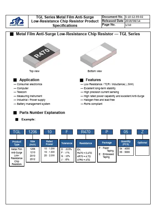
■Metal Film Anti-Surge Low-Resistance Chip Resistor — TGL SeriesTop view Bottom view■Application█Features— Consumer electronics — Low Resistance / TCR / Inductance(≦5nH)— Computer — Excellent long-term stability— Telecom — High precision current sensing— Measuring instrument — High rated power capability and excellent Anti-Surge — Industrial / Power supply — Halogen free and lead free— Battery management system — RoHs compliant■Parts Number Explanation■Example:Final Milestone DateCheckpointTGL1206F R470P05Size (Inch) 1206 1210 2010 2512ToleranceD:±0.5%F:±1%G:±2%J:±5%PackageP:PaperT apingE:EmbossedT apingQuantity(PCS)04:400005:5000ZOptionalProductTypeMetal Film Anti-SurgeLow-ResistanceChip ResistorsResistanceEX.R470=0.47Ω4R70=4.7Ω47R0=47Ω10RatedPower10:1.0W15:1.5W20:2.0W■Standard Electrical SpecificationsType RatedPowerat 70℃Max.RatedCurrentMax.OverloadCurrentT.C.R.(ppm/℃)Resistance RangeD(0.5%), F(1.0%), G(2.0%), J(5.0%)TGL1206 1W 3.16A 7.07A±50 100 mΩ ≦R ≦50 ΩTGL1210 1W 3.16A 7.07ATGL2010 1.5W 3.87A 8.66A±50 100 mΩ ≦R ≦50 ΩTGL2512 2W 4.47A 10.00A● For non-standard parts, please contact our sales dept.● Operating Temperature Range :−55℃〜+155℃.■Anti-Surge Ability:■Type Dimension■Construction Unit:mmTYPE L W H I1I2 TGL1206 3.10±0.10 1.60±0.10 0.55±0.10 0.40±0.20 0.45±0.20 TGL1210 3.10±0.10 2.50±0.15 0.55±0.10 0.50±0.20 0.50±0.20 TGL2010 5.00±0.20 2.50±0.15 0.55±0.10 0.60±0.25 0.60±0.25 TGL2512 6.30±0.20 3.20±0.20 0.55±0.10 0.65±0.25 0.65±0.25①Alumina Substrate ⑥Top Protective Overcoat②Resistive Layer ⑦Marking③Bottom Inner Electrode (Cu) ⑧Side Inner Electrode④Top Inner Electrode ⑨Barrier Layer (Ni)⑤Bottom Protective OvercoatWhite⑩Solder coating (Sn)■ Perfo r mance CharacteristicsPower Derating Curve ■The Operating Temperature Range: -55°C ~+155°C.Power rating or current rating is in the case based on continuous full-load at ambient temperature of 70℃. For operation at ambient temperature in excess of 70℃, the load should be derated in accordance with figure of derating Curve.■ Rated CurrentResistance Range: ≦ 1ΩRated Current: The resistor shall have a DC continuous working current or a AC (rms) continuous working current at commercial-line frequency and wave form corresponding to the power rating, as determined formula as following:I = Rated current (A) P= Rated Power (W) R= Resistance(Ω)■ Rated VoltageResistance Range: > 1ΩRated Voltage: The resistor shall have a DC continuous working voltage or a RMS AC continuous working voltage at commercial-line frequency and wave form corresponding to the power rating, as determined formula as following:V = Rated voltage (V)V = √P ×R P = Rated power (W)R = Nominal resistance (Ω)-5520406080100020406080100120140155℃Ambient Temperature (℃)Power Ratio(%)DERATING CURVE70160■Reliability Test and RequirementTest Item Test Method Procedure Requirements TemperatureCoefficient of Resistance(T.C.R) JIS C 5201-1clause 4.8TCR +125 ℃, 25 ℃is the reference temperatureRefer to StandardElectrical SpecificationsShort Time Overload JIS C 5201-1clause 4.135 times rated power for 5 seconds. ±(1.0%+0.001Ω)Insulation Resistance JIS C 5201-1clause 4.6100V for 1 minute. ≧10GΩDielectric Withstanding Voltage JIS-C5201-1clause 4.71206、1210、2010、2512 for 500 VAC 1minNo short or burned on theappearance.Core Body Strength JIS-C5201-1clause 4.15Central part pressurizing force:10N , 10 seconds No brokenSolderability JIS C 5201-1clause 4.17245±5°C for 3±0.5secs.>95% CoverageNo Visual damageResistance to Soldering Heat JIS-C5201-1clause 4.181. Molten solder, 260±5 °C,10±1 seconds immersion time2. IR reflow, refer to solder reflow temperature condition±(1.0%+0.001Ω)No Visual damageLeaching JIS-C5201-1clause 4.18260±5℃for 30 seconds.>95% CoverageNo Visual damageTemperature Cycling JIS C 5201-1clause 4.19-55℃to +155℃, 300 cycles±(1.0%+0.001Ω)No Visual damageLoad Life in Humidity JIS C 5201-1clause 4.2440±2℃, 90~95% R.H. , Rated power or Max. workingcurrent whichever is less for 1000 hrs with 1.5 hrs〝ON〞and 0.5 hr〝OFF〞.±(1.0%+0.001Ω)Load Life (Endurance) JIS C 5201-1clause 4.2570±2℃, Rated power, or Max. working current whichever isless for 1000 hrs with 1.5 hrs〝ON〞and 0.5 hr〝OFF〞.±(1.0%+0.001Ω)High Temperature Exposure JIS C 5201-1clause 4.25155±5℃for 1000 +48/-0 hours. ±(1.0%+0.001Ω)Resistance to Solvent JIS C 5201-1clause 4.29The tested resistor be immersed into isopropyl alcohol of20~25℃for 60 secs.Then the resistor is left in the room for 48 hrs.±(1.0%+0.001Ω)No Visual damageTerminal Strength JIS-C5201-1clause 4.32Pressurizing force for 10 seconds1206 and above:17.7NNo brokenTerminal Bending Strength JIS C 5201-1clause 4.33Bending once for 5 secondsD:1206、1210 = 3mm2010、2512 = 2mm±(1.0%+0.001Ω)No Visual damage● Temperature Coefficient of Resistance test to - 55 ℃is available on request■MarkingSolder reflow Temperature condition■Appendix For SMD Chip ResistorSIZE A ΦB ΦC■Packaging Information■Tapping SpecificationUnit: mm Packaging Type A B W E F G H T ΦD PPaper Type1206 1.90±0.2 3.05±0.28.0±0.2 1.75±0.1 3.5±0.05 4.0±0.1 2.0±0.050.75±0.1 4.0±0.11210 2.85±0.2 3.05±0.28.0±0.2 1.75±0.1 3.5±0.05 4.0±0.1 2.0±0.050.75±0.1 4.0±0.1■Embossed DimensionUnit: mm Packaging Type A B W E F G H T ΦDΦD1T1 PEmbossedType 2010 2.80±0.25.60±0.212±0.1 1.75±0.15.5±0.05 4.0±0.1 2.0±0.050.23±0.1 1.50±0.10.85±0.15 4.0±0.1 2512 3.40±0.2 6.70±0.212±0.1 1.75±0.15.5±0.05 4.0±0.1 2.0±0.050.23±0.1 1.50±0.10.85±0.15 4.0±0.1PaperCarrier■ Packing Material Data / Storage Data■ Front & Back Lead Dimension■ Top Adhesive Peel Off Strength :10~70g■ PackageInner Box Size Reel Size H(mm) 1 13 2 24 3 36 5 60 10113■ Storage Data :Storage time at the environment temp: 25±5℃& humidity: 60±20% is valid for one year from the date of delivery. External Box SizeContain (Kpcs) Length (mm)Width (mm)Width (mm)25K 180 180 60 50K 180 180 110 150K 430 200 200 300K400400200。
金属膜电阻
详细信息:
详细信息:
详细信息:
详细信息:
金属膜电阻器就是以特种金属或合金作电阻材料,用真空蒸发或溅射的方法,在陶瓷或玻璃基本上形成电阻膜层的电阻器。
这类电阻器一般采用真空蒸发工艺制得,即在真空中加热合金,合金蒸发,使瓷棒表面形成一层导电金属膜。
刻槽和改变金属膜厚度可以控制阻值。
它的耐热性、噪声电势、温度系数、电压系数等电性能比碳膜电阻器优良。
金属膜电阻器的制造工艺比较灵活,不仅可以调整它的材料成分和膜层厚度,也可通过刻槽调整阻值,因而可以制成性能良好,阻值范围较宽的电阻器。
这种电阻和碳膜电阻相比,体积小、噪声低、稳定性好,但成本较高,常常作为精密和高稳定性的电阻器而广泛应用,同时也通用于各种无线电电子设备中。
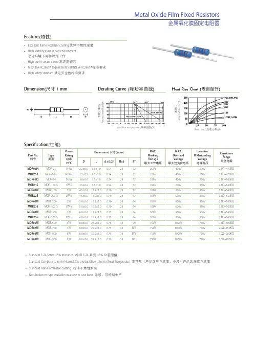
Feature (特性)•Excellent flame retardant coating 优异不燃性涂装 •High stability even in bad environment 恶劣环境下同样稳定工作•High purity ceramic core 高纯度瓷芯•Meet EIA-RC2655A requirements 满足EIA-RC2655A 标准要求•High safety standard 满足安全性标准要求Dimension(尺寸)mm Derating Curve (降功率曲线)Metal Oxide Film Fixed Resistors金属氧化膜固定电阻器Heat Rise Chart (表面温升)P e r c e n t r a t e d l o a d (%)Rated load (负载比率) (%)T e m p e r a t u r e r i s e (°C )Ambient temperature (环境温度)(°C)负载比率(%)温升(°C )Specification(性能)Part No.料号Type 类型Power Rating 功率70°C Dimension (尺寸)(mm)MAX.Working Voltage 最大工作电压MAX.Overlaod Voltage 最大过负荷电压Dielectric Withstanding Voltage 绝缘耐压Resistance Range 阻值范围D L d ±0.05H±3PT MOR0W4MOR-251/4W 2.2±0.5 6.5±1.00.542852250V 400V 250V 0.1Ω~470KΩMOR0S2MOR-50-S 1/2W-S 2.2±0.5 6.5±1.00.542852250V 400V 250V 0.1Ω~470KΩMOR0W2MOR-501/2W 3.0±0.69.5±1.00.542852250V 400V 250V 0.1Ω~560KΩMOR01S MOR-100-S 1W-S 3.5±0.69.5±1.00.542852350V 600V 350V 0.1Ω~560KΩMOR01W MOR-1001W 4.5±0.611.5±1.00.702852350V 600V 350V 0.1Ω~560KΩMOR02S MOR-200-S 2W-S 4.5±0.611.5±1.00.702852350V 600V 350V 0.1Ω~560KΩMOR02W MOR-2002W 5.0±0.615.5±1.00.702864350V 600V 350V 0.1Ω~560KΩMOR03S MOR-300-S 3W-S 5.0±0.615.5±1.00.702864350V 600V 350V 0.1Ω~560KΩMOR03W MOR-3003W 6.0±0.617.5±1.00.752864500V 800V 500V 0.1Ω~560KΩMOR05S MOR-500-S 5W-S 6.0±0.617.5±1.00.752864500V 800V 500V 0.1Ω~560KΩMOR05W MOR-5005W 8.0±0.624.5±1.00.753890750V 1000V 750V 0.1Ω~680KΩMOR07W MOR-7007W 8.0±0.629.5±1.00.7538B/B 750V 1000V 750V 20Ω~150KΩMOR08W MOR-8008W 8.0±0.639.5±1.00.7538B/B 750V 1000V 750V 30Ω~200KΩMOR09WMOR-9009W8.0±0.652.5±1.00.7538B/B750V1000V750V50Ω~200KΩ•Standard E-24 Series ±5% tolerance 标准E-24系列±5% 公差阻值•Standard Gray base color for Normal Size product,Blue color for Small Size product 正常尺寸产品涂灰色底漆,小尺寸产品涂海蓝色底漆•Standard Non-Flammable coating 标准不燃性涂装•Non-Inductive type available on a case to case basis 无感,可特别生产Performance Specification(性能)Metal Oxide Film Fixed Resistors金属氧化膜固定电阻器Temperature coefficient 温度系数1/4W,1/2WS: ≤ 100K Ω:±350PPM/°C ; 100KΩ<R≤470KΩ:0~-700PPM/°C 1/2W,1WS: ≤ 120K Ω:±350PPM/°C ; 120KΩ<R≤560KΩ:0~-700PPM/°C1W,2W,2WS,3W,3WS,5WS: ≤ 150K Ω:±350PPM/°C ; 150KΩ<R≤560KΩ:0~-700PPM/°C 5W,: ≤ 180K Ω:±350PPM/°C ; 180KΩ<R≤680KΩ:0~-700PPM/°C 7W,8W ,9W: ±350PPM/°CShort-time Overload短时间过负荷Normal size(正常尺寸),ΔR/R ≤ ±(1%+0.05 Ω), with no evidence of mechanical damage (无可见机械损伤) Small size(小尺寸),ΔR/R ≤ ±(2%+0.05 Ω), with no evidence of mechanical damage (无可见机械损伤)Dielectric withstanding voltage绝缘耐压No evidence of flashover,mechanical damage,arcing or insulation breakdown ( 无击穿、飞弧及可见机械损伤)Pulse Overload 脉冲过负荷Normal size(正常尺寸),ΔR/R ≤ ±(2%+0.05 Ω), with no evidence of mechanical damage (无可见机械损伤) Small size(小尺寸),ΔR/R ≤ ±(5%+0.05 Ω), with no evidence of mechanical damage (无可见机械损伤)Terminal strength 端子强度No evidence of mechanical damage ( 无可见机械损伤)Soldering heat 耐焊接热ΔR/R ≤ ±(1%+0.05 Ω), with no evidence of mechanical damage (无可见机械损伤)Solderability 可焊性Min.95% coverage (最少95%覆盖率)Resistance to solvent 耐熔剂No deterioration of protective coating and markings (包封层,色码完整)Temperature cycling 温度循环ΔR/R ≤ ±(2%+0.05 Ω)with no evidence of mechanical damage (无可见机械损伤)Humidity ( Steady State )恒定湿热ΔR/R ≤ ±(2%+0.05 Ω)with no evidence of mechanical damage (无可见机械损伤)Load life in humidity湿度寿命< 100kΩ : ±(5%+0.05Ω)MAX ,≥100kΩ :±(10%+0.05Ω) MAX;Load life负载寿命< 100kΩ : ±(5%+0.05Ω)MAX ,≥100kΩ :±(10%+0.05Ω) MAX;Flame retardant阻燃Resistor insulation is self-extinguishing within 10 seconds after externally applied flame is removed (火焰移开后10秒内,电阻自动绝燃,无可见火焰)。
插件电阻规格表1. 引言插件电阻是电子电路中常见的被动元件之一,用于调节电路中的电阻值。
在电子产品的设计和制造中,插件电阻规格表是非常重要的参考文档。
本文将介绍插件电阻规格表的内容和使用方法。
2. 插件电阻规格表的结构插件电阻规格表通常包含以下几个方面的信息:2.1 电阻值范围插件电阻的电阻值通常以欧姆(Ω)为单位表示,规格表中会列出电阻值的范围。
这个范围可以从几个欧姆到几百万欧姆不等,根据实际需要选择合适的电阻值。
2.2 容差插件电阻的容差是指实际电阻值与标称电阻值之间的允许误差范围。
容差通常以百分比表示,规格表中会列出容差的最大值。
较常见的容差包括1%、5%和10%等。
2.3 功率插件电阻的功率是指电阻器能够承受的最大功率。
功率通常以瓦特(W)为单位表示,规格表中会列出功率的数值。
常见的功率有1/8W、1/4W和1/2W等。
2.4 封装尺寸插件电阻的封装尺寸是指电阻器的外形尺寸,包括长度、宽度和高度等。
规格表中会列出电阻器的尺寸,以便在设计电路时能够合理安排元件的布局。
2.5 温度系数插件电阻的温度系数是指电阻值随温度变化的程度。
温度系数通常以每摄氏度(ppm/°C)表示,规格表中会列出温度系数的数值。
常见的温度系数有50ppm/°C和100ppm/°C等。
3. 使用插件电阻规格表使用插件电阻规格表需要注意以下几个方面:3.1 选择合适的电阻值根据电路设计的需要,选择合适的电阻值范围。
如果需要精确的电阻值,可以选择容差较小的电阻器。
3.2 确定合适的容差根据电路设计的要求,确定合适的容差范围。
容差较小的电阻器价格较高,容差较大的电阻器价格较低。
3.3 考虑功率要求根据电路中电阻器的功率消耗,选择合适的功率。
功率较大的电阻器可以承受较高的功率,但体积较大。
3.4 确认封装尺寸根据电路中的布局需求,确认插件电阻的封装尺寸。
尺寸较小的电阻器可以节省空间,但功率承受能力较低。
插件电阻规格表摘要:1.插件电阻简介2.插件电阻规格表的组成3.插件电阻参数及其意义4.插件电阻的选择与应用5.总结正文:插件电阻,作为一种常见的电子元器件,广泛应用于各种电子产品和电子设备中。
为了帮助大家更好地了解和选择插件电阻,本文将为您详细解析插件电阻规格表及其相关参数。
一、插件电阻简介插件电阻,又称可调电阻、可调电位器,是一种具有固定电阻值或可调电阻值的电子元器件。
插件电阻主要用于调整电路中的电阻值,以满足不同电路需求。
它具有体积小、性能稳定、安装方便等特点。
二、插件电阻规格表的组成插件电阻规格表通常包括以下几个部分:电阻值、电阻误差、功率、额定电压、工作温度等。
这些参数可以帮助用户了解插件电阻的性能和特点,为电路设计提供参考依据。
三、插件电阻参数及其意义1.电阻值:插件电阻的基本参数,表示电阻器对电流的阻碍程度。
电阻值越小,电流通过越容易。
2.电阻误差:表示电阻值与标准值之间的差异。
电阻误差越小,电阻值的稳定性越高。
3.功率:插件电阻所能承受的最大功率。
功率越大,表示插件电阻在电路中能承受的电流越大。
4.额定电压:插件电阻所能承受的最大电压。
额定电压越高,表示插件电阻在高压电路中的稳定性越高。
5.工作温度:插件电阻正常工作的环境温度范围。
工作温度范围越宽,表示插件电阻在不同环境温度下的稳定性越高。
四、插件电阻的选择与应用在选择插件电阻时,需要根据实际电路需求,综合考虑电阻值、电阻误差、功率、额定电压、工作温度等因素。
选择合适的插件电阻,能够提高电路的性能和稳定性。
插件电阻广泛应用于各种电子产品和电子设备中,如音响、电视、计算机、通信设备等。
通过调整插件电阻的电阻值,可以实现音量调节、亮度调节、信号处理等功能。
总之,插件电阻规格表是了解插件电阻性能和特点的重要依据。
在选择插件电阻时,需要综合考虑电阻值、电阻误差、功率、额定电压、工作温度等因素,确保插件电阻满足实际电路需求。
2016/12/15viking 金属氧化膜电阻MOF 系列2485封装功率高达7W 【捷比信科技】/info/20141481.html 1/1毫欧电阻主要特性参数电阻器的工艺问题探索电子元器件与电商的大时代电动汽车电池管理系统的工作原理台湾viking 光颉耐高压贴片电阻HVR 系列最大工作电压可达3000V 行业利好:致使扭扭车下架的相关专利存在专利无效可能机械行业:无人机 渐行渐近的蓝海市场TCL 乐视宣布战略合作 推动产业升级 共谋全球电视市场小型可穿戴健康设备的兴起将成就大数据viking 抗冲击电阻SWR 系列首页 > 行业资讯 > viking金属氧化膜电阻MOF系列2485封装功率高达7Wviking金属氧化膜电阻MOF系列2485封装功率高达7W捷比信 MOF 系列金属氧化膜插件电阻具有优良的长期稳定性 ,高浪涌/过载能力,电气和机械稳定性和高可靠性。
阻值范围宽:0.1Ω~ 22MΩ,电阻标准公差±5%、±2%、±1% ,封装可选0623/0932/1145 1550/1765/2485,工作温度范围55 ~ +155°C ,功率最大可达7W 应用领域 -汽车 -电信 -医疗设备 查货,索样请来电洽询深圳市捷比信科技有限公司。
C: BY:陆 TIME:20161214随机推荐:知识版权所有 © 深圳市捷比信科技有限公司服务热线:+8675529796190 传真:+8675529796149 地址:深圳市龙华新区东环一路皇嘉中心A 座820822 Email :sales@电阻产品: 低温漂电阻 大毅电阻 Viking 光颉电阻 高精密低温漂电阻 采样电阻 大功率无感电阻 插件精密电阻 高频电感 汽车专用电阻 贴片保险丝 低温漂精密电阻 毫欧电阻 排阻泰艺晶振产品: 有源晶振 晶振封装 晶振频率 晶振精度 32.768K 晶振 恒温晶振 高温晶振 可编程晶振 温补晶振 压控晶振 无源晶振 贴片晶振 插件晶振 钟振 石英振荡器 晶振波形输出 SCcut 切晶振ALPS 代理产品: ALPS 编码器 ALPS 电位器 ALPS 开关按键 ALPS 卡座连接器 ALPS TACT Switch网站统计走进捷比信大毅(TA-I)光颉(Viking)阿尔卑斯(ALPS)公司简介资讯信息联系我们。
MO 金属氧化膜电阻器Ⅰ:尺 寸额定功率: 1 W 负载负荷曲线:如FIG .1、FIG .2阻 值: 0.68 Ω 色环标示:A: 蓝 B: 灰 C: 银 D: 金精度等级: J 级 ±5%Ⅱ:规格尺寸尺 寸 ( 毫米 )阻 值 范 围功 率最高使用电压 最高过负荷电压耐电压型 号 E F GMO-100 1W 、2WS 500V 1000V 700V P 、T/B 11.00 0.5±0.02 3.8±0.5MO-200 2W 、3WS 500V 1000V 1000V P 、T/B 15.00 0.7±0.02 5.0±0.5MO-300 3W 、5WS 500V 1000V 1000V P 、T/B 17.00 0.8±0.02 6.0±0.5ST ANDARD1Ω-10MEGⅢ:电气特性测 试 项 目测试方法T estCondition规格Spec 使用温度范围 -30℃~+155℃ ±350PPM/℃ 短 时 间 过 负荷 2.5倍额定电压、测试5秒±(2%+0.05Ω)耐 久 性 温度70℃,加额定电压开1.5小时,关0.5小时循环1000小时 ±(5%+0.05Ω)耐 电 压 最大耐电压测试1分钟 ±(0.5%+0.05Ω)温 度 循 环 温度-25℃~+85℃ 5次循环±(2%+0.05Ω)绝 缘 阻 抗 将待测试物置V 型槽施加500V 直流电压 1000 M Ω 耐 湿 负 荷 温度40℃,温度95%加额定电压1.5小时,关0.5小时,循环1000小时 ±(5%+0.05Ω)耐 热 性 温度350℃时间3.5秒 ±(2%+0.05Ω)焊 锡 性 温度235℃时间5秒 >95% 继 续 过 负 荷4倍额定电压加1秒,停25秒循环10000次±(5%+0.05Ω)Ⅳ:包装标准注:1、最小采购量为1000PCS=1K规格 1W 2WS 2W 3WS最小包装(PCS)2000 2000 1000 1000 盒装(包)2000 2000 1000 1000 编带包装(PCS)无无无无Ⅴ:色环电阻对照表第一色环第二色环第三色环第四色环色环颜色第一位数字第二位数字倍乘误差范围100=1 ×1Ω±1% 黑— 0棕 1 1101=10×10Ω±2%102=100×100Ω±3% 红 2 2103=1000×1KΩ±4% 橙 3 3黄 4 4104=10000×10KΩ—105=100000×100KΩ±0.5% 绿 5 5蓝 6 6106=1000000×1MΩ±0.2%107=10000000×10MΩ±0.1% 紫 7 7108=100000000×100MΩ—灰 8 8白 9 9109=1000000000×1000MΩ—金—— 10-1=0.1 ×0.1Ω±5%银—— 10-2=0.01 ×0.01Ω±10% 无色————±20%Ⅵ:外包装盒规格如图:功率包装数量 Wmm Lmm Hmm1W 2000PCS 85.00 260.00 105.002WS 2000PCS 85.00 260.00 105.002W 1000PCS 85.00 260.00 105.003WS 1000PCS 85.00 260.00 105.00。
mo金属膜电阻【原创实用版】目录1.mo 金属膜电阻的概述2.mo 金属膜电阻的特点3.mo 金属膜电阻的性能4.mo 金属膜电阻的应用领域5.mo 金属膜电阻的发展前景正文一、mo 金属膜电阻的概述mo 金属膜电阻,全称为金属膜电阻,是一种以金属膜为电阻材料的电阻器。
金属膜电阻具有精度高、稳定性好、体积小、噪音低等优点,广泛应用于电子设备、仪器仪表、通讯设备等领域。
二、mo 金属膜电阻的特点1.高精度:金属膜电阻采用金属膜作为电阻材料,具有较高的电阻精度,可以满足各种精度要求。
2.稳定性好:金属膜电阻的材料稳定性好,使得其电阻值在一定温度范围内变化较小,从而保证了电阻值的稳定性。
3.体积小:金属膜电阻采用薄膜技术制作,具有较小的体积,便于安装和使用。
4.噪音低:金属膜电阻的材料内部结构紧密,电阻值分布均匀,因此具有较低的噪音。
三、mo 金属膜电阻的性能1.线性:金属膜电阻的电阻值随电压、电流的变化而变化,具有良好的线性特性。
2.温度系数:金属膜电阻的温度系数较低,使得其电阻值随温度的变化较小。
3.功率:金属膜电阻具有较高的功率承受能力,可以承受较大的功率。
四、mo 金属膜电阻的应用领域1.电子设备:金属膜电阻广泛应用于各种电子设备中,如计算机、电视机、收音机等。
2.仪器仪表:金属膜电阻在各种仪器仪表中具有重要应用,如测量仪器、信号发生器等。
3.通讯设备:金属膜电阻在通讯设备中也有广泛应用,如电话机、传真机等。
五、mo 金属膜电阻的发展前景随着科技的发展,对电阻器的要求越来越高。
金属膜电阻具有精度高、稳定性好、体积小、噪音低等优点,符合现代电子技术的发展趋势。