Resistor.Today-CSFR系列取样电阻规格书
- 格式:pdf
- 大小:4.27 MB
- 文档页数:3

目录1. 电阻的定义及工作原理 (2)2. 电阻的阻值及读法 (3)3. 电阻的分类 (6)●按伏安特性分类 (6)●按材料分类 (6)●特殊电阻器 (7)4. 电阻的功能 (8)●端接 (9)●分压电路 (12)●限流电路 (12)●阻抗匹配电路 (13)●RC充放电电路 (14)●上拉/下拉电阻 (15)5. 电阻的超导现象 (17)1.电阻的定义及工作原理定义:电阻器(Resistor)在日常生活中一般直接称为电阻。
是一个限流元件,将电阻接在电路中后,电阻器的阻值是固定的一般是两个引脚,它可限制通过它所连支路的电流大小。
阻值不能改变的称为固定电阻器。
阻值可变的称为电位器或可变电阻器。
理想的电阻器是线性的,即通过电阻器的瞬时电流与外加瞬时电压成正比。
用于分压的可变电阻器。
在裸露的电阻体上,紧压着一至两个可移金属触点。
触点位置确定电阻体任一端与触点间的阻值。
端电压与电流有确定函数关系,体现电能转化为其他形式能力的二端器件,用字母R来表示,单位为欧姆Ω。
实际器件如灯泡,电热丝,电阻器等均可表示为电阻器元件。
原理:电阻器由电阻体、骨架和引出端三部分构成(实芯电阻器的电阻体与骨架合二为一),而决定阻值的只是电阻体。
对于截面均匀的电阻体,电阻值为电阻值式中ρ为电阻材料的电阻率(欧·厘米);L为电阻体的长度(厘米);A为电阻体的截面积(平方厘米)。
薄膜电阻体的厚度d很小,难于测准,且ρ又随厚度而变化,故把视为与薄膜材料有关的常数,称为膜电阻。
实际上它就是正方形薄膜的阻值,故又称方阻(欧/方)。
对于均匀薄膜薄膜阻值式中W为薄膜的宽度(厘米)。
通常Rs应在一有限范围内,Rs太大会影响电阻器性能的稳定。
因此圆柱形电阻体以刻槽方法,平面形电阻体用刻蚀迂回图形的方法来扩大其阻值范围,并进行阻值微调。
伏安特性是用图形曲线来表示电阻端部电压和电流的关系,当电压电流成比例时(特性为直线),称为线性电阻,否则称为非线性电阻。
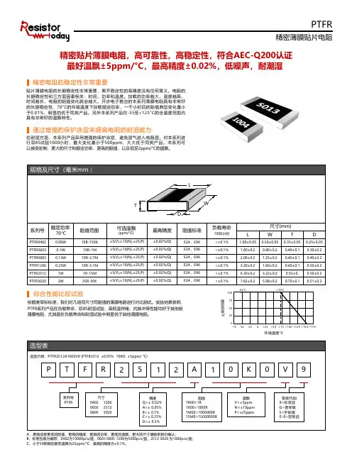
PZFR精密箔技术贴片电阻高精密表贴电阻,金属箔技术,最高工作温度+175°C温飘±2ppm/°C ,最高精度±0.01%,高耐湿能力,天然低噪声抗脉冲能力强,抗静电,极好货架寿命及负载寿命高精密和高稳定性应该一起来讨论才具有实际的意义。
无论是膜式的电阻还是合金的电阻,通过精密的调阻工艺都可以达到很高的初始精度。
但电阻在使用前要经过运输,存储,焊接等过程,这些过程都会造成电阻阻值的变化。
另外电阻需要在不同的环境温度下工作,同时加载功率也会使电阻产生自热,这些因素都会使阻值发生不可逆的变化。
高精密的电阻必须同时具有高稳定性的特点。
电阻的稳定性比初始精度更重要最快24小时交货,无最小起定量限制开步电子常备箔电阻芯片,可以满足小批量快速交付。
从用户下单到发货最快24小时完成,1且不设最小订购量,即使1片也可以订购。
每只箔电阻出厂前都经过严格的测试程序,确保符合性能指标。
不受阻值标准约束,可任意定义需要的阻值每只箔电阻都要经过调阻,通过切断边缘区域的调阻带从而增加阻值,达到调整阻值的目的。
和其他电阻不同,用户可以任意的定义阻值,不受标准阻值的约束,比如1.234欧。
备箔芯片库存可以在关注“开步电子微服平台”,进入箔电阻库存查询。
常① 根据不同的使用温度范围,我们可以定制最低+/-1ppm 的温飘。
PZFR精密箔技术贴片电阻额定功率%环境温度°C1007550250-55°C +70°C-75-50-250+25+50+75+100+125+150+175在需要选择一个具有长期稳定性的电阻的时候,几个因素需要被考虑。
这些因素包括:温度系数(TCR ), 功率系数(PCR ), 负载寿命,寿命末期精度,噪声,热电势,抗静电能力。
PZFR 系列箔电阻基于全新的Z1箔技术生产,Z1箔技术在原有Z 箔技术的基础上改进了绑定层和保护层,极大的改善了电阻的稳定性和耐湿能力,使得该电阻可以在很宽的温度范围内工作。
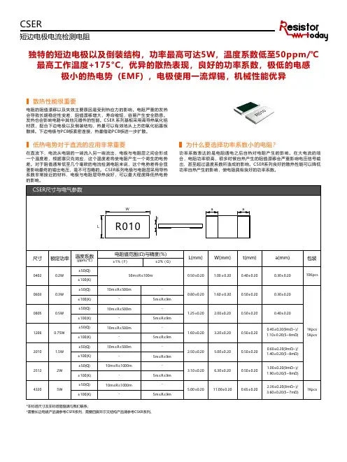
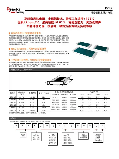
CSER短边电极电流检测电阻独特的短边电极以及倒装结构,功率最高可达5W ,温度系数低至50ppm/℃最高工作温度+1 75°C ,优异的散热表现,良好的功率系数,极低的电感极小的热电势(EMF ),电极使用一流焊锡,机械性能优异散热性能很重要低热电势对于直流的应用非常重要为什么要选择功率系数小的电阻?*非标准尺寸及非标准阻值请与我们联系;*需要长边电极产品请参考CSFR 系列,需要四脚开尔文结构产品请参考CSKR 系列。
电阻的阻值漂移以及失效主要原因是受到热应力的影响。
电阻严重的发热会导致长期稳定性变差,阻值漂移增大,寿命缩短,容易产生安全隐患。
发热也会影响电路中其他元器件的性能。
CSER 系列基板采用高导热氧化铝材质,配合下边电极以及倒装结构,热量可以有效地从上方的氧化铝基板散掉。
下边电极与PCB 板紧密连接,热量借助PCB 板进一步扩散。
在直流下,电流从电阻的一端流入另一端流出,电极与电阻层之间会形成一个温度差,根据塞贝克效应,这个温度差将使电阻产生一个寄生的电势差。
对于阻值通常低至几个毫欧的电流检测电阻来说,这个电势差将会显著影响最终的输出电压,是不可忽略的。
CSER 系列电极与电阻层采用导热系数非常接近的材料,电极与电阻层导热良好,可以最大程度降低热电势的影响。
功率系数表达的是电阻通电之后自热对电阻产生的影响。
在大电流的场合,电阻功率很高,很多时候自热产生的阻值漂移会严重影响电压信号输出,甚至超过温度系数所造成的影响。
CSER 系列良好的散热性能可以降低功率自热产生的影响,使电阻具有良好的功率系数。
CSER短边电极电流检测电阻1206尺寸CSER系列箔技术电阻和同尺寸合金电阻加载1W功率后的发热对比CSER 系列串联电感参数(单位:pH)竞争对手产品 CSER 系列低电感产品CSER0805-R005CSER0805-R010膜式检流电阻合金电阻测试条件 : -55℃ 30 分钟 → 室温 3 分钟 → 155℃ 30 分钟 → 室温 3 分钟,循环3000 由于热胀冷缩,PCB 会对电阻造成拉伸或挤压。
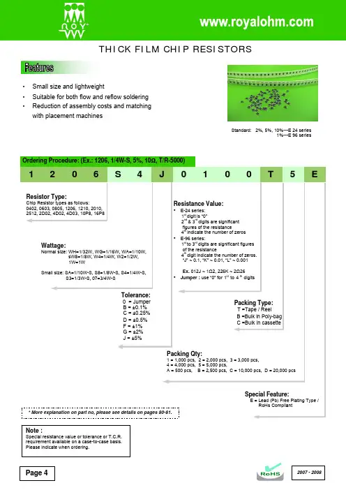
Page 4•Small size and lightweight• Suitable for both flow and reflow soldering •Reduction of assembly costs and matching with placement machines2007 - 2008Standard: 2%, 5%, 10%---E 24 series 1%---E 96 series2007 - 2008 Page 5Marking on the Resistors Body:•For 0402 size, no marking on the body due to the small size of the resistor.•±5% tolerance product. (Including resistance values less than 1Ω; both 1% and 5%) The marking is 3 digits, the first 2 digits are the significant figures of the resistance and the 3rd digit denotes number of zeros.153 = 15000Ω = 15KΩ; 120 = 12Ω Below 10Ω shown as this: 6R8 = 6.8Ω 0.1Ω~0.99Ω shown as this: R33 = 0.33Ω•±1% tolerance marking of case size 0805 and bigger is 4 digits, the first 3 digits are the significant figures of the resistance and the 4th digit denotes number of zeros.2372 = 23700Ω = 23.7KΩ; 1430 = 143Ω Below 10Ω shown as this: 3R24 = 3.24Ω0.1Ω~0.99Ω shown as this: R33 = 0.33ΩPage 62007 - 2008* More details, please see pages 78-79.• Standard E-96 series values (±1% tolerance) of 0603 size. Due to the small size of the resistor’s body, 3 digitsmarking will be used to indicate the accurate resistance value by using the Multiplier code & Standard E-96 Series Resistance Value Code as shown on Page 6.1.96K Ω = 196 x 101 Ω = 29B12.4Ω = 124 x 10-1 Ω = 10X• Standard E-24 series values which does not belong to E-96 series values (in ±1% tolerance) of 0603 size. The marking is the same as 5% tolerance but marked with underline.122 = 1200 = 1.2K Ω680 = 68ΩTemperature coefficient±5%: 1Ω ~ 10M Ω ≤ ±200PPM/°C±1%: 10Ω ~ 100Ω ≤ ±200PPM/°C; 101Ω ~ 1M Ω ≤ ±100PPM/°C Short-time overload ±5%: ±(2.0% + 0.1Ω) Max. ±1%: ±(1.0% + 0.1Ω) Max. Insulation resistanceMin. 1,000 Mega OhmDielectric withstanding voltageNo evidence of flashover, mechanical damage, arcing or insulation breakdown Terminal bending ±(1.0% + 0.05Ω) Max.Soldering heat Resistance change rate is ±(1.0% + 0.05Ω) Max. SolderabilityMin. 95% coverage Temperature cycling ±5%: ±(1.0% + 0.05Ω) Max. ±1%: ±(0.5% + 0.05Ω) Max. Humidity (Steady State) ±5%: ±(3.0% + 0.1Ω) Max. ±1%: ±(0.5% + 0.1Ω) Max. Load life in humidity±5%: ±(3.0% + 0.1Ω) Max. ±1%: ±(1.0% + 0.1Ω) Max. Load life±5%: ±(3.0% + 0.1Ω) Max.±1%: ±(1.0% + 0.1Ω) Max.* The values which are not of standard E-24 series (2% & 5%) and not of E-96 series (1%) could be offered on a case to case basis.2007 - 2008Page 72007 - 2008Page 8•16P8 (16Pin 8R)THICK FILM CHIP RESISTOR ARRAYS• High density 2, 4, 8 resistors in one small case (convex type) • Improvement of placement efficiency• Packaging is suitable for automatic placement machines • Superior solderability • Scalloped•2D02 (4Pin 2R)•4D02, 4D03 (8Pin 4R)•10P8 (10Pin 8R)Part No.StyleLWHℓ1ℓ2PQ2D02 (0402x2) 2D02 (4Pin 2R) 1.0 ± 0.1 1.0 ± 0.1 0.35 ± 0.1 0.17 ± 0.1 0.25 ± 0.1 0.65 ± 0.05 0.33 ± 0.1 4D02 (0402x4) 4D02 (8Pin 4R) 2.0 ± 0.1 1.0 ± 0.1 0.45 ± 0.1 0.2 ± 0.15 0.3 ± 0.15 0.5 ± 0.05 0.3 ± 0.05 4D03 (0603x4) 4D03 (8Pin 4R) 3.2 ± 0.2 1.6 ± 0.2 0.5 ± 0.1 0.3 ± 0.15 0.3 ± 0.15 0.8 ± 0.1 0.5 ± 0.15 16P8 16P8 (16Pin 8R) 4.0 ± 0.2 1.6 ± 0.15 0.45 ± 0.1 0.3 ± 0.15 0.4 ± 0.15 0.5 ± 0.05 0.3 ± 0.05 10P8 10P8 (10Pin 8R)3.2 ± 0.21.6 ± 0.150.55 ± 0.10.4 ± 0.10.3 ± 0.150.64 ± 0.050.35 ± 0.05Resistance RangePart No. StylePower Rating at 70ºC Max. Working Voltage Max. Overload VoltageDielectric With-standing VoltageOperated Temp. RangeF (±1%) E-96 seriesJ (±5%) E-24 seriesJumper Rated Current2D02 2D02 (4Pin2R) 1/16W 50V 100V 500V -55ºC~+155ºC - 10Ω~ 1M Ω - 4D02 4D02 (8Pin4R) 1/16W 50V 100V 500V -55ºC~+155ºC -10Ω~ 1M Ω -4D03 4D03 (8Pin4R) 1/16W 50V 100V 500V -55ºC~+155ºC 100Ω~560K Ω 10Ω~ 1M Ω 1A 16P8 16P8 (16Pin8R) 1/16W 50V 100V 100V -55ºC~+155ºC - 10Ω~ 1M Ω - 10P810P8 (10Pin8R)1/32W 25V 50V 50V -55ºC~+155ºC -33Ω~ 100K Ω -Note: Part number and ordering procedure the same as Thick Film Chip Resistors on Page 4.Standard: 2%, 5%, 10%---E 24 series 1%---E 96 series。
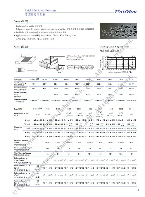
• Small size & light weight 短小轻薄• Reduction of assembly costs and matching with placement machine. 可降低装置成本及配合机器组装• Suitable for both wave & re-flow soldering. 适合波峰焊与回流焊• Applications: Navigator (GPS), Mobile Phone,Telecom, PDA, Setbox, Meter. 应用于GPS , 移动电话,PDA ,机顶盒,仪表Feature (特性)Figures (型状)Derating Curve & Specification降功率曲线及性能Thick Film Chip ResistorsP e r c e n t r a t e d l o a d (%)Ambient termperature 环境温度 (°C)厚膜晶片电阻器负载比率(%)UniOhm3r i g h s e rv ed .©UValue阻值Code 代码Value 阻值Code 代码Value 阻值Code 代码Value 阻值Code 代码Value 阻值Code 代码Value 阻值Code 代码100011471721533316494646568181102021501822134324504756669882105031541922635332514876771583107041582023236340524996873284110051622123737348535116975085113061652224338357545237076886115071692324939365555367178787118081742425540374565497280688121091782526141383575627382589124101822626742392585767484590127111872727443402595907586691130121912828044412606047688792133131962928745422616197790993137142003029446432626347893194140152053130147442636497995395143162103230948453646658097696Thick Film Chip Resistors• For 0201 & 0402 size, no marking on the body due to the small size of the resistor. 0201, 0402因电阻本体太小,故本体无标示字码• ±5% tolerance product: the marking is 3 digits, the first 2 digits are the significant of theresistance and the 3rd digit denotes number of zeros following.±5%公差产品字码是三位数,前二位是阻值的有效数,第三位表示有几个 0• 0805, 1206, 1210, 2010, 2512 ≤±1%: the marking is 4 digits, the first 3 digits are the significant of the resistance and the 4th digit denotes number of zeros following. 0805, 1206, 1210, 2010, 2512 ≤±1%公差产品字码有四位数,前三位是阻值的有效数,第四位表示有几个 0Marking on the Resistors Body (电阻本体字码标示)2372 = 23700Ω = 23.7KΩBelow 10Ω : 3R24 = 3.24Ω10Ω 以下标示: 3R24 = 3.24Ω153 = 15000Ω = 15KΩBelow 10Ω: 6R8 = 6.8Ω10Ω 以下标示: 6R8 = 6.8Ω• Standard E-96 series values of 0603 ≤±1%: due to the small size of the resistor’s body, 3 digits marking will be used to indicate the accurate resistance value by using the following Multiplier & Resistance Code.0603 ≤±1%公差 E-96系列标准阻值,因电阻本体太小,采用三位阻值代码(数字)及下列指数代码(字母)配合来指明标准的阻值。
热敏电阻residual resistance参数
热敏电阻的参数有:
1.允差电阻值Rc:一般指环境温度为25℃时热敏电阻器的具体电阻值。
2.具体电阻值RT:在一定的温度标准下所测出的电阻值。
3.原材料常数:它是一个叙述热敏电阻材料物理特点的主要参数,也是热敏感度指标值,B值越大,表达热敏电阻器的敏感度越高。
4.电阻器温度系数αT:它表达温度转变1℃时的电阻值弹性系数,企业为%/℃。
5.时间常数τ:热敏电阻器是有热惯性力的,时间常数,便是一个叙述热敏电阻器热惯性力的主要参数。
6.最大功率PM:在要求的技术性标准下,热敏电阻器长期性持续负荷所容许的失配输出功率。
PreparedContentsIntroduction ………………………………………………………………………………………Page1.0 Scope (4)2.0 Ratings & Dimension ………………………………………………………….…………....4~53.0 Structure.................................... (5)4.0 Marking…….…………………………………… ………………………. ..… …………… 6~75.0 Derating Curve................................................... .. (8)6.0 Performance Specification …………………………………………….……………..........8~97.0 Explanation of Part No. System ………………………………….…………………………9~108.0 Ordering Procedure (10)9.0 Standard Packing ………………………………………………….…………………………11~1210.0 Note Matter.................................................................. . (12)File Name:CHIP SERIES±0.5%,±1%,±2%,±5%& 0ΩDate 2014.05.23EditionNo. 1Amendment Record Signature Edition Prescription of amendment Amend Page Amend Date Amended by Checked by1.0 Scope:This specification for approve relates to the Lead-Free Thick Film Chip Resistors manufactured byROYALOHM.2.0 Ratings & Dimension:01005、0201、0402 0603、0805、1206、1210、1812、2010、25122.1 Dimension & Resistance Range :Type70℃ PowerDimension(mm) Resistance RangeL W H A B 0.5% 1.0% 2.0% 5.0%01005 1/32W 0.40±0.02 0.20±0.02 0.13±0.02 0.10±0.050.10±0.03--10Ω-10M Ω 10Ω-10M Ω10Ω-10M Ω0201 1/20W 0.60±0.03 0.30±0.03 0.23±0.03 0.10±0.050.15±0.05-- 1Ω-10M Ω 1Ω-10M Ω1Ω-10M Ω0402 1/16W 1.00±0.100.50±0.05 0.35±0.05 0.20±0.100.25±0.101Ω-10M Ω0.2Ω~22M Ω 0.2Ω~22M Ω0.2Ω~22M Ω06031/16W 1/10WS 1.60±0.10 0.80±0.10 0.45±0.10 0.30±0.200.30±0.201Ω-10M Ω0.1Ω~33M Ω 0.1Ω~33M Ω0.1Ω~100M Ω0805 1/10W 1/8WS 2.00±0.15 +0.151.25-0.10 0.55±0.10 0.40±0.200.40±0.201Ω-10M Ω0.1Ω~33M Ω 0.1Ω~33M Ω0.1Ω~100M Ω1206 1/8W 1/4WS 3.10±0.15 +0.151.55-0.100.55±0.10 0.45±0.200.45±0.201Ω-10M Ω0.1Ω~33M Ω 0.1Ω~33M Ω0.1Ω~100M Ω1210 1/4W1/3WS 1/2WSS3.10±0.10 2.60±0.20 0.55±0.10 0.50±0.250.50±0.201Ω-10M Ω0.1Ω~10M Ω 0.1Ω~22M Ω0.1Ω~100M Ω18121/2W 3/4WS 4.50±0.20 3.20±0.20 0.55±0.20 0.50±0.200.50±0.200.1Ω-10M Ω0.1Ω-10M Ω 0.1Ω-10M Ω0.1Ω-10M Ω2010 1/2W 3/4WS5.00±0.10 2.50±0.20 0.55±0.10 0.60±0.250.50±0.201Ω-10M Ω0.1Ω~22M Ω 0.1Ω~22M Ω0.1Ω~22M Ω2512 1W 6.35±0.10 3.20±0.20 0.55±0.10 0.60±0.250.50±0.201Ω-10M Ω0.1Ω~33M Ω 0.1Ω~33M Ω0.1Ω~33M Ω2.2 RatingsType70℃PowerMax 。
RoHS CompliantType02010402060308051206121020102512Max. Working Voltage 25V 50V 50V 150V 200V 200V 200V 200VMax. Overload Voltage50V 100V 100V 300V 400V 400V 400V 400V Dielectric withstanding Voltage -100V300V500V500V500V500V500VOperating Temperature-55~+155°C -55~+155°C -55~+155°C -55~+155°C -55~+155°C -55~+155°C -55~+155°C -55~+155°CType02010402060308051206121020102512Power Rating at 70°C1/20W 1/16W 1/16W (1/10W-S)1/10W (1/8W-S)1/8W (1/4W-S)1/4W (1/3W-S) *1/2W (3/4W-S)1W L (mm)0.60 ± 0.03 1.00 ± 0.10 1.60 ± 0.10 2.00 ± 0.15 3.10 ± 0.15 3.10 ± 0.10 5.00 ± 0.10 6.35 ± 0.10W (mm)0.30 ± 0.030.50 ± 0.050.80+0.15 -0.101.25+0.15 -0.101.55+0.15 -0.102.60+0.15 -0.102.50+0.15 -0.103.20+0.15 -0.10DimensionH (mm)0.23 ± 0.030.35 ± 0.050.45 ± 0.100.55 ± 0.100.55 ± 0.100.55 ± 0.100.55 ± 0.100.55 ± 0.10A (mm)0.10 ± 0.050.20 ± 0.100.30 ± 0.200.40 ± 0.200.45 ± 0.200.50 ± 0.250.60 ± 0.250.60 ± 0.25B (mm)0.15 ± 0.050.25 ± 0.100.30 ± 0.200.40 ± 0.200.45 ± 0.200.50 ± 0.200.50 ± 0.200.50 ± 0.20Resistance Value of Jumper <50mΩ<50mΩ<50mΩ<50mΩ<50mΩ<50mΩ<50mΩ<50mΩRated Current of Jumper 0.5A 1A 1A 2A 2A 2A 2A 2A Max. Current of Jumper 1A 2A 2A 5A 10A 10A 10A 10A Resistance Range of 0.5% (E-96)10Ω ~ 1MΩ1Ω ~ 10MΩ1Ω ~ 10MΩ1Ω ~ 10MΩ1Ω ~ 10MΩ1Ω ~ 10MΩ1Ω ~ 10MΩ1Ω ~ 10MΩResistance Range of 1% (E-96)10Ω ~ 1MΩ1Ω ~ 10MΩ1Ω ~ 10MΩ1Ω ~ 10MΩ1Ω ~ 10MΩ1Ω ~ 10MΩ1Ω ~ 10MΩ1Ω ~ 10MΩResistance Range of 2% (E-24)10Ω ~ 1MΩ1Ω ~ 10MΩ1Ω ~ 10MΩ1Ω ~ 10MΩ1Ω ~ 10MΩ1Ω ~ 10MΩ1Ω ~ 10MΩ1Ω ~ 10MΩResistance Range of 5% (E-24)1Ω ~ 1MΩ1Ω ~ 10MΩ1Ω ~ 10MΩ1Ω ~ 10MΩ1Ω ~ 10MΩ1Ω ~ 10MΩ1Ω ~ 10MΩ1Ω ~ 10MΩ* 1210 size in 1/2W could be provided specially (1210U2)• Small size & light weight• Reduction of assembly costs and matching with placement machine • Suitable for both flow & re-flow soldering• Applications: Navigator (GPS), Mobile Phone,Telecom, PDA, Setbox, Meter.FeatureFiguresDerating Curve & SpecificationThick Film Chip ResistorsP e r c e n t r a t e d l o a d (%)Ambient termperature(°C )2UniOhmRoHS CompliantValue Code Value Code Value Code Value Code Value Code Value Code100011471721533316494646568181102021501822134324504756669882105031541922635332514876771583107041582023236340524996873284110051622123737348535116975085113061652224338357545237076886115071692324939365555367178787118081742425540374565497280688121091782526141383575627382589124101822626742392585767484590127111872727443402595907586691130121912828044412606047688792133131962928745422616197790993137142003029446432626347893194140152053130147442636497995395143162103230948453646658097696Thick Film Chip Resistors• For 0201 & 0402 size, no marking on the body due to the small size of the resistor.• ±5% tolerance product: the marking is 3 digits, the first 2 digits are the significant of the resistance and the 3rd digit denotes number of zeros following.• 0805, 1206, 1210, 2010, 2512 ±1%: the marking is 4 digits, the first 3 digits are the signivicant of the resistance and the 4th digit denotes number of zeros following.Marking on the Resistors Body2372 = 23700Ω = 23.7KΩ; 1430 = 143ΩBelow 10Ω : 3R24 = 3.24Ω153 = 15000Ω = 15KΩ; 120 = 12ΩBelow 10Ω: 6R8 = 6.8Ω• Standard E-96 series values of 0603 ±1%: due to the small size of the resistor’s body, 3 digits marking will be used to indicate the accurate resistance value by using the following Multiplier & Resistance Code.Multiplier Code (for 0603 1% marking)So the resistance value are marked as the following examples:1.96KΩ= 196 ×101 Ω = 29B12.4Ω= 124 ×10 -1 = 10X• Standard E-24 and not belong to E-96 series values (±1%) of 0603 size: the marking is te same as 5% tolerance but marking as underline.122 = 1200 = 1.2 KΩ680 = 68ΩStandard E-96 Series Resistance Value Code (for 0603 1% marking)Code A B C D E F G H X Y Z Multiplier10010110210310410510610710-110-210-3UniOhm3RoHS CompliantTemperature coefficiant1Ω~10Ω ≤ ±400PPM/°C11Ω~100Ω ≤ ±200PPM/°C>100Ω ±100PPM/°C (0201: >100Ω ±200PPM/°C ) Short-time overload±5%, ± 2%: ±(2.0% + 0.1Ω) Max.±1%, ± 0.5%: ±(1.0% + 0.1Ω) Max. Insulation resistance≥ 1,000 Mega OhmDielectronic withstanding voltageNo evidence of flashover, mechanical damage, arcing or insulation breakdown Terminal bending ±(1.0% + 0.05Ω) Max. Solering heat ±(1.0% + 0.05Ω) Max. Solerability Min. 95% coverageTemperature cycling±5%, ± 2%: ±(1.0% + 0.05Ω) Max.±1%, ± 0.5%: ±(0.5% + 0.05Ω) Max. Humidity (Steady State)±5%, ± 2%: ±(3.0% + 0.1Ω) Max.±1%, ± 0.5%: ±(0.5% + 0.1Ω) Max. Load life in humidity±5%, ± 2%: ±(3.0% + 0.1Ω) Max.±1%, ± 0.5%: ±(1.0% + 0.1Ω) Max. Load life±5%, ± 2%: ±(3.0% + 0.1Ω) Max.±1%, ± 0.5%: ±(1.0% + 0.1Ω) Max.• The values which are not of standard E-24 series (2% & 5%) and not of E-96 series (1%) could be offered on a case to case basis.Special Feature:E = Lead Free (standard)Resistance Value : 5% (E-24 series):the 1st digit is “0”, the 2nd & 3rd digits are for the significant figures of the resistance and the 4th indicate the numbers of zeros following; 1% (E-96 series):the 1st to 3rd digits are for the signifi-cant figures of the resistance and the 4th indicate the numbers of zeros following.Tolerance:F = ±1%G = ±2%J = ±5%R =0~30%: Q =0~20%:N =-20~0%P =-30~0%:K =±10%:M =±20%:Wattage:Fill-in 2 digits with the codes as fol-low:WH=1/32W WM=1/20W , WG=1/16W , WA=1/10W , 1W=1W , W2=1/2W W4=1/4W , W8=1/8W , SA=1/10W-S, S8=1/8W-S, S4=1/4W-S, S3=1/3W-S, U2=1/2W-SS 07=3/4W-SProduct Type:Fill-in 4 digits with the Chip resistor type as follow:0201, 0402, 0603, 0805, 1206, 1210, 2010, 2512, 2D02, 2C02, 4D02, 4C02, 4D03, 4C03, 16P8, 10P8, 10S8, 10T8, 10E9, TR05, TR06, HP03, HP05, HP06, CS12, 1218, 0612, 1020.Ordering Procedure (Example: 1206 1/4W-S 5% 1.2 Ω T/R-5000)Performance SpecificationsThick Film Chip Resistors4UniOhm。
CSFR
长边电极低阻采样电阻
独特的长边电极以及倒装结构,功率最高可达10W ,温度系数低至50ppm/℃最高工作温度+1 75°C ,优异的散热表现,良好的功率系数,极低的电感
极小的热电势(EMF ),电极使用一流焊锡,机械性能优异
散热性能很重要
低热电势对于直流的应用非常重要
为什么要选择功率系数小的电阻?
*非标准尺寸及非标准阻值请与我们联系;
*需要短边电极产品请参考CSER 系列,需要四脚开尔文结构产品请参考CSKR 系列。
电阻的阻值漂移以及失效主要原因是受到热应力的影响。
电阻严重的发热会导致长期稳定性变差,阻值漂移增大,寿命缩短,容易产生安全隐患。
发热也会影响电路中其他元器件的性能。
CSFR 系列基板采用高导热氧化铝材质,配合下边电极以及倒装结构,热量可以有效地从上方的氧化铝基板散掉。
下边电极与PCB 板紧密连接,热量借助PCB 板进一步扩散。
在直流下,电流从电阻的一端流入另一端流出,电极与电阻层之间会形成一个温度差,根据塞贝克效应,这个温度差将使电阻产生一个寄生的电势差。
对于阻值通常低至几个毫欧的电流检测电阻来说,这个电势差将会显著影响最终的输出电压,是不可忽略的。
CSFR 系列电极与电阻层采用导热系数非常接近的材料,利用长边电极的特点增大接触面积,电极与电阻层导热良好,可以最大程度降低热电势的影响。
在直流下,电流从电阻的一端流入另一端流出,电极与电阻层之间会形成一个温度差,根据塞贝克效应,这个温度差将使电阻产生一个寄生的电势差。
对于阻值通常低至几个毫欧的电流检测电阻来说,这个电势差将会显著影响最终的输出电压,是不可忽略的。
CSFR 系列电极与电阻层采用导热系数非常接近的材料,利用长边电极的特点增大接触面积,电极与电阻层导热良好,可以最大程度降低热电势的影响。
CSFR
长边电极低阻采样电阻
1206尺寸CSFR系列箔技术电阻和同尺寸合金电阻加载1W功率后的发热对比
CSFR 系列串联电感参数(单位:pH)竞争对手产品 CSFR 系列低电感产品
CSFR0805-R005
CSFR0805-R010
膜式检流电阻合金电阻
测试条件 : -55℃ 30 分钟 → 室温 3 分钟 → 155℃ 30 分钟 → 室温 3 分钟,循环3000 由于热胀冷缩,PCB 会对电阻造成拉伸或挤压。
通过本实验对比不同电阻科技对抗机械应力的能力
优异的引脚机械强度
CSFR 金属箔贴片检流电阻C S F R 002K 9
选型表
选型示例: CSFR2512GR002K9 (CSFR2512 ±2% 2mR ±100ppm)系列号
CSFR
尺寸
06030805 1206 CSFR
长边电极低阻采样电阻。