棒状玻璃釉膜高压电阻(RI80)规格书
- 格式:pdf
- 大小:411.59 KB
- 文档页数:4

VR25000003303JA 100VR37000003904JA100VR25000008204JA100VR37000002005FA100VR37000002204FA100VR25, VR37, VR68Vishay BCcomponentsHigh Ohmic / High Voltage Metal Glaze Leaded ResistorsDESIGN SUPPORT TOOLSA metal glazed film is deposited on a high grade ceramic body. After a helical groove has been cut in the resistive layer, tinned electrolytic copper wires are welded to the end-caps. The resistors are coated with a light blue lacquer which provides electrical, mechanical, and climatic protection.FEATURES•UL Approved (UL1676, file no: E171160)•Meet the safety requirements of:-IEC 60065-DIN EN 60065-VDE 0860-CQC (China)•AEC-Q200 qualified (VR25, VR37)•High pulse loading capability (maximum 10 kV)•Radial version available for VR25•Material categorization: for definitions of compliance please see /doc?99912APPLICATIONS•Where high resistance, high stability, and high reliability at high voltage are required •High humidity environment •White goods •Power supplies •Automotive electronicsNote(1)Ohmic values (other than resistance range) are available on requestTECHNICAL SPECIFICATIONSDESCRIPTION VR25VR37VR68Imperial size 020*********Resistance range (1)100 k Ω to 22 M Ω100 k Ω to 33 M Ω100 k Ω to 68 M ΩResistance tolerance ± 10 %; ± 5 %; ± 1 %Temperature coefficient ≤ ± 200 ppm/KRated dissipation, P 700.25 W 0.5 W 1.0 W Operating voltage, U max. AC/DC 1600 V 3500 V 10 000 V Operating temperature range -55 °C to +155 °CPeak permissible film temperature 155 °C Thermal resistance (R th )140 K/W 120 K/W70 K/W Insulation voltage:1 min.; U ins700 V Maximum noise (white noise)5 μV/V 2.5 μV/V 2.5 μV/V Max. resistance change atrated dissipation for resistance range, |∆R /R | max., after 1000 h1.5 %1.5 %1.5 %SAFETY REQUIREMENTS AND QUALIFICATIONSDESCRIPTIONVR25, VR37VR37VR68Safety requirements / qualifications AEC-Q200UL1676 qualification (file no: E171160)for ohmic range 510 k Ω to 11 M Ω;DIN EN 60065 (VDE 0860): 2015; clause 14.2 a);EN 60065: 2014IEC 60065: clause 14.2 a)CQCVR25, VR37, VR68Vishay BCcomponentsNote(1)See table “Temperature Coefficient and Resistance Range” for selecting correct ohmic value - tolerance combinationTEMPERATURE COEFFICIENT AND RESISTANCE RANGETYPE TCRTOLERANCERESISTANCE E-SERIES VR25≤ ± 200 ppm/K± 1 %100 k Ω to 15 M ΩE24; E96± 5 %100 k Ω to 22 M ΩE24; E96± 10 %15 M Ω to 22 M ΩE24VR37± 1 %100 k Ω to 33 M ΩE24; E96± 5 %100 k Ω to 33 M ΩE24VR68± 1 %100 k Ω to 68 M ΩE24; E96± 5 %100 k Ω to 68 M ΩE24PART NUMBER AND PRODUCT DESCRIPTIONPART NUMBER: VR25000001003FA100TYPE / SIZE VARIANT TCR RESISTANCE TOLERANCE (1)PACKAGINGSPECIAL VR25000 = VR25VR37000 = VR37VR68000 = VR680 = neutral0 = standard3 digit value 1 digit multiplier MULTIPLIER 0 = *1001 = *1012 = *1023 = *1034 = *1045 = *1056 = *106F = ± 1 %J = ± 5 %K = ± 10 %A1AC A5RD R5N400 = standardPRODUCT DESCRIPTION: VR25 1 % A1 100KVR25 1 %A1100K TYPE / SIZETOLERANCE PACKAGINGRESISTANCE VR25VR37VR68± 1 %± 5 %± 10 %A1AC A5RD R5N4100K = 100 k Ω15M = 15 M ΩPACKAGINGTYPECODE QUANTITY PACKAGING STYLEWIDTH PITCH DIMENSIONS VR25A11000Taped according to IEC 60286-1 fan-folded in a box 53 mm 5 mm 75 mm x 31 mm x 260 mm A5500053 mm 5 mm 76 mm x 105 mm x 265 mm N44000Taped according to IEC 60286-2 fan-folded in a box-12.7 mm 48 mm x 253 mm x 330 mm R55000Taped according to IEC 60286-1 on a reel 53 mm 5 mm 93 mm x 300 mm x 298 mm VR37A11000Taped according to IEC 60286-1 fan-folded in a box53 mm 5 mm 72 mm x 60 mm x 258 mm R55000Taped according to IEC 60286-1 on a reel 53 mm 5 mm 90 mm x 375 mm x 375 mm VR68AC 500Taped according to IEC 60286-1 fan-folded in a box66 mm 10 mm 82 mm x 111 mm x 256 mm RD750Taped according to IEC 60286-1 on a reel66 mm10 mm105 mm x 315 mm x 305 mmV R 5000001003F A 1002VR25, VR37, VR68 Vishay BCcomponentsDESCRIPTIONProduction is strictly controlled and follows an extensive set of instructions established for reproducibility. A homogeneous film of metal alloy is deposited on a high grade ceramic body and conditioned to achieve the desired temperature coefficient. Plated steel termination caps are firmly pressed on the metalized rods. Mostly, a special laser is used to achieve the target value by smoothly cutting a helical groove in the resistive layer without damaging the ceramics. Connecting wires of electrolytic copper plated with 100 % pure tin are welded to the termination caps. The resistor elements are covered by a light blue protective coating designed for electrical, mechanical, and climatic protection. Four or five color code rings designate the resistance value and tolerance in accordance with IEC 60062.Yellow and gray are used instead of gold and silver because metal particles in the lacquer could affect high-voltage properties.The result of the determined production is verified by an extensive testing procedure performed on 100 % of the individual resistors. Only accepted products are stuck directly on the adhesive tapes in accordance with IEC 60286-1 or for the radial versions in accordance to IEC 60286-2.MATERIALSVishay acknowledges the following systems for the regulation of hazardous substances:•IEC 62474, Material Declaration for Products of and for the Electrotechnical Industry, with the list of declarable substances given therein (1)•The G lobal Automotive Declarable Substance List (GADSL) (2)•The REACH regulation (1907/2006/EC) and the related list of substances with very high concern (SVHC) (3) for its supply chainThe products do not contain any of the banned substances as per IEC 62474, G ADSL, or the SVHC list, see /how/leadfree.Hence the products fully comply with the following directives:•2000/53/EC End-of-Life Vehicle Directive (ELV) and Annex II (ELV II)•2011/65/EU Restriction of the Use of Hazardous Substances Directive (RoHS) with amendment 2015/863/EU•2012/19/EU Waste Electrical and Electronic Equipment Directive (WEEE)Vishay pursues the elimination of conflict minerals from its supply chain, see the Conflict Minerals Policy at /doc?49037.ASSEMBLYThe resistors are suitable for processing on automatic insertion equipment and cutting and bending machines. Excellent solderability is proven, even after extended storage. They are suitable for automatic soldering using wave or dipping.The resistors are completely lead (Pb)-free, the pure tin plating provides compatibility with lead (Pb)-free and lead-containing soldering processes. The immunity of the plating against tin whisker growth, in compliance with IEC 60068-2-82, has been proven under extensive testing. The encapsulant is resistant to cleaning solvent specified in IEC 60115-1. The suitability of conformal coatings, if applied, shall be qualified by appropriate means to ensure the long-term stability of the whole system.APPROVALSThese resistors meet the safety requirements of:•UL1676 (510 kΩ to 11 MΩ); file no: E171160•IEC 60065, clause 14.2 a)•DIN EN 60065, clause 14.2 a)•VDE 0860, clause 14.2 a)•CQC, ChinaRELATED PRODUCTSFor a correlated range of Metal Film Resistors see the datasheet:“High Ohmic / High Voltage Metal Film Leaded Resistors”, /doc?30260For product that offers high power dissipation and metal oxide film technology see the datasheet:“High Power Metal Oxide Leaded Resistors”,/doc?20128Notes(1)The IEC 62474 list of declarable substances is maintained in a dedicated database, which is available at http://std.iec.ch/iec62474(2)The G lobal Automotive Declarable Substance List (G ADSL) is maintained by the American Chemistry Council, and available atVR25, VR37, VR68Vishay BCcomponentsFUNCTIONAL PERFORMANCEDeratingHot-Spot Temperature Rise ( T) as a Function of Dissipated PowerVR25VR37VR25, VR37, VR68 Vishay BCcomponentsMaximum allowed peak pulse voltage in accordance with IEC 60065, 14.2 a);50 discharges from a 1nF capacitor charged to Ûmax.; 12 discharges/min (drift ∆R/R≤ 2 %)VR25VR37VR25, VR37, VR68 Vishay BCcomponentsTemperature Rise ( T) at the Lead End (Soldering Point) as a Function of Dissipated Power at Various Lead Lengths after MountingVR25VR37VR25, VR37, VR68Vishay BCcomponentsTESTS PROCEDURES AND REQUIREMENTSAll tests are carried out in accordance with the following specifications:•IEC 60115-1, generic specification (includes tests)The test and requirements table contains only the most important tests. For the full test schedule refer to the documents listed above.The tests are carried out with reference to IEC 60115-1, in accordance with IEC 60068-2-xx test method and under standard atmospheric conditions in accordance with IEC 60068-1, 5.3.A climatic category 55 / 155 / 56 is applied, defined by the lower category temperature (LCT = -55 °C), the upper category temperature (UCT = 155 °C), and the duration of exposure in the damp heat, steady state test (56 days).Unless otherwise specified the following values apply:•Temperature: 15 °C to 35 °C •Relative humidity: 45 % to 75 %•Air pressure: 86 kPa to 106 kPa (860 mbar to 1060 mbar).For performing some of the tests, the components are mounted on a test board in accordance with IEC 60115-1, 4.31.In test procedures and requirements table, only the tests and requirements are listed with reference to the relevant clauses of IEC 60115-1 and IEC 60068-2-xx test methods. A short description of the test procedure is also given.TESTS PROCEDURES AND REQUIREMENTSIEC 60115-1 CLAUSE IEC 60068-2TEST METHOD TESTPROCEDUREREQUIREMENTS PERMISSIBLE CHANGE(∆R max.)4.6.1.1Insulation resistanceU max. DC = 500 V during 1 min; V-block methodR ins min.: 10 000 M Ω4.7Voltage proof U RMS = U ins ; 60 sNo breakdown or flashover4.8Temperature coefficientAt (20 / -55 / 20) °C and (20 / 155 / 20) °C≤ ± 200 ppm/K 4.12NoiseIEC 60195VR25: max. 5 μV/V VR37: max. 2.5 μV/V VR68: max. 2.5 μV/V 4.13Short time overload Room temperature; 2.5 x ;(voltage not more than 2 x limiting voltage);10 cycles; 5 s ON and 45 s OFF∆R max.: ± 2 % R 4.1621 (Ua1)21 (Ub)21 (Uc)Robustness of terminationsTensile, bending, and torsionNo damage ∆R max.: ± 0.5 % R4.1720 (Ta)Solderability+235 °C; 2 s; solder bath method; SnPb40+245 °C; 3 s; solder bath method; SnAg3Cu0.5(before aging)Good tinning (≥ 95 % covered);no damage+235 °C; 2 s; solder bath method; SnPb40+245 °C; 3 s; solder bath method; SnAg3Cu0.5(after aging)Good tinning (≥ 95 % covered);no damage4.1820 (Tb)Resistance to soldering heat Unmounted components (260 ± 5) °C; (10 ± 1) s∆R max.: ± 0.5 % R 4.1914 (Na)Rapid change of temperature30 min at -55 °C and 30 min at +155 °C;5 cycles ∆R max.: ± 0.5 % R 4.2029 (Eb)Bump 3 x 1500 bumps in 3 directions; 40 g No damage ∆R max.: ± 0.5 % R 4.226 (Fc)Vibration 10 sweep cycles per direction;10 Hz to 2000 Hz;1.5 mm or 200 m/s 2No damage ∆R max.: ± 0.5 % R4.23Climatic sequence:R ins min.: 1 G Ω∆R max.: ± 1.5 % R4.23.2 2 (Bb)Dry heat 16 h; 155 °C 4.23.330 (Db)Damp heat cyclic 24 h; 25 °C to 55 °C;90 % to 100 % RH4.23.4 1 (Ab)Cold 2 h; -55 °C 4.23.513 (M)Low air pressure 2 h; 8.5 kPa;15 °C to 35 °C4.23.630 (Db)Damp heat remaining cyclic5 days; 55 °C;95 % to 100 % RH; 5 cycles P 70 x RVR25, VR37, VR68Vishay BCcomponentsDIMENSIONSVR25 WITH RADIAL TAPINGLead Spacing (F = 4.8 mm), Size 02074.2478 (Cab)Damp heat(steady state)56 days; 40 °C;90 % to 95 % RH; loaded with 0.01 P 70(steps: 0 V to 100 V)∆R max.: ± 1.5 % R 4.25.1Endurance (at 70 °C)1000 h; loaded with P 70 or U max.;1.5 h ON and 0.5 h OFF ∆R max.: ± 1.5 % R 4.26Active flammability “cheese-cloth test”Steps of:5 / 10 / 16 / 25 / 40 x P 70 duration 5 minVR25: no flaming of gauze cylinder VR68: no flaming of gauze cylinder 4.35Passive flammability “needle-flame test”Application of test flame for 20 sNo ignition of product;no ignition of under-layer;burning time less than 30 sDIMENSIONS - Leaded resistor types, mass, and relevant physical dimensionsTYPE Ø D max. (mm)L 1 max. (mm)L 2 max. (mm)Ø d (mm)MASS (mg)VR25 2.5 6.57.50.58 ± 0.05212VR37 4.09.010.00.70 ± 0.03457VR686.818.019.00.78 ± 0.051690TESTS PROCEDURES AND REQUIREMENTSIEC 60115-1 CLAUSE IEC 60068-2TEST METHOD TEST PROCEDUREREQUIREMENTS PERMISSIBLE CHANGE(∆R max.)L dDIMENSIONS in millimetersPitch of components P 12.7 ± 1.0Lead spacing F 4.8 + 0.7 / - 0.0Width of carrier tape W 18.0 ± 0.5Body to hole centerH 19.5 ± 1.0Height for cutting (max.)L 11Height for bending H 016.5 ± 0.5Component height (max.)H 129VR25, VR37, VR68 Vishay BCcomponentsHISTORICAL 12NC INFORMATION•The resistors have a 12-digit numeric code starting with -2322 241 refers to VR25-2322 242 refers to VR37-2322 244 refers to VR68•The subsequent first digit for 1 % tolerance products (E24 and E96 series) or 2 digits for 5 % (E24 series) and 10 % (E12 series) indicate the resistor type and packing•The remaining digits indicate the resistance value:-The first 3 digits for 1 % or 2 digits for 5 % and 10 % tolerance products indicate the resistance value-The last digit indicates the resistance decadeLast Digit of 12NC Indicating Resistance DecadeHistorical 12NC Example•The 12NC for a VR25, resistor value 7.5 MΩ, 5 % tolerance, supplied on a bandoleer of 1000 units in ammopack, is: 2322 241 13755.•The 12NC for a VR37, resistor value 7.5 MΩ, 5 % tolerance, supplied on a bandoleer of 1000 units in ammopack, is: 2322 242 13755.•The 12NC for a VR68, resistor value 7.5 MΩ, 5 % tolerance, supplied on a bandoleer of 500 units in ammopack, is: 2322 244 13755.RESISTANCE DECADE LAST DIGIT100 kΩ to 976 kΩ41 MΩ to 9.76 MΩ5≥ 10 MΩ612NC CODING FOR VR25, VR37, VR68 - Resistor type and packagingTYPE TOLERANCE(%)VR25 CODING STARTS WITH 2322 241 .....VR37 CODING STARTS WITH 2322 242 .....VR68 CODING STARTS WITH 2322 244 .....BANDOLIER IN AMMOPACK BANDOLIER ON REEL RADIAL TAPED STRAIGHT LEADS4000 UNITS52 mm52 mm66.7 mm52 mm66.7 mm1000 UNITS5000 UNITS500 UNITS5000 UNITS750 UNITSVR25± 10....8....7....- 6....-± 536...13...53...-23...-± 1038...12...52...-22...-VR37± 1-8....-- 6....-± 5-13...--23...-VR68± 1---8....- 6....± 5---13...-23...Legal Disclaimer Notice VishayDisclaimerALL PRODUCT, PRODUCT SPECIFICATIONS AND DATA ARE SUBJECT TO CHANGE WITHOUT NOTICE TO IMPROV E RELIABILITY, FUNCTION OR DESIGN OR OTHERWISE.V ishay Intertechnology, Inc., its affiliates, agents, and employees, and all persons acting on its or their behalf (collectively,“Vishay”), disclaim any and all liability for any errors, inaccuracies or incompleteness contained in any datasheet or in any other disclosure relating to any product.Vishay makes no warranty, representation or guarantee regarding the suitability of the products for any particular purpose or the continuing production of any product. To the maximum extent permitted by applicable law, Vishay disclaims (i) any and all liability arising out of the application or use of any product, (ii) any and all liability, including without limitation special, consequential or incidental damages, and (iii) any and all implied warranties, including warranties of fitness for particular purpose, non-infringement and merchantability.Statements regarding the suitability of products for certain types of applications are based on Vishay's knowledge of typical requirements that are often placed on Vishay products in generic applications. Such statements are not binding statements about the suitability of products for a particular application. It is the customer's responsibility to validate that a particular product with the properties described in the product specification is suitable for use in a particular application. Parameters provided in datasheets and / or specifications may vary in different applications and performance may vary over time. All operating parameters, including typical parameters, must be validated for each customer application by the customer's technical experts. Product specifications do not expand or otherwise modify Vishay's terms and conditions of purchase, including but not limited to the warranty expressed therein.Hyperlinks included in this datasheet may direct users to third-party websites. These links are provided as a convenience and for informational purposes only. Inclusion of these hyperlinks does not constitute an endorsement or an approval by Vishay of any of the products, services or opinions of the corporation, organization or individual associated with the third-party website. Vishay disclaims any and all liability and bears no responsibility for the accuracy, legality or content of the third-party website or for that of subsequent links.Except as expressly indicated in writing, Vishay products are not designed for use in medical, life-saving, or life-sustaining applications or for any other application in which the failure of the Vishay product could result in personal injury or death. Customers using or selling Vishay products not expressly indicated for use in such applications do so at their own risk. Please contact authorized Vishay personnel to obtain written terms and conditions regarding products designed for such applications. No license, express or implied, by estoppel or otherwise, to any intellectual property rights is granted by this document or by any conduct of Vishay. Product names and markings noted herein may be trademarks of their respective owners.© 2022 VISHAY INTERTECHNOLOGY, INC. ALL RIGHTS RESERVEDRevision: 01-Jan-20221Document Number: 91000VR68000001003JA C00VR68000001504JA C00VR25000003303JA 100VR37000003904JA100VR25000008204JA100VR37000002005FA100VR37000002204FA100。
贴片玻璃釉电阻-概述说明以及解释1.引言1.1 概述贴片玻璃釉电阻是一种常见的电子元件,广泛应用于电路板及其他电子设备中。
其主要特点是外观小巧,安装方便,能够在各种环境条件下可靠地工作。
在电子产品的制造中,贴片玻璃釉电阻扮演着重要的角色。
本文将对贴片玻璃釉电阻的定义和原理进行详细介绍,以帮助读者更好地理解其工作原理和应用场景。
同时,还将介绍贴片玻璃釉电阻的特点和优势,以及其在电子领域的一些常见应用。
在正文部分,我们将首先介绍贴片玻璃釉电阻的定义和原理。
贴片玻璃釉电阻采用玻璃釉材料作为电阻体,并结合特定的工艺制作而成。
其具有较高的稳定性和精准的电阻值,能够在广泛的温度范围内工作。
接着,我们将探讨贴片玻璃釉电阻的特点和应用。
贴片玻璃釉电阻具有体积小、重量轻、功耗低等优点,适用于各种电子设备的紧凑空间。
在通信设备、计算机、汽车电子等领域,贴片玻璃釉电阻被广泛应用于电路板的布线、电流限制、电压分压等功能中。
最后,我们将对贴片玻璃釉电阻进行总结和评价,并提出未来的发展方向和研究建议。
在技术不断进步的背景下,贴片玻璃釉电阻的性能和应用也在不断提升,未来有望更加广泛地应用于各个领域。
通过本文的阐述,我们希望读者能够对贴片玻璃釉电阻有更深入的了解,为电子设备的设计和应用提供参考和指导。
1.2文章结构1.2 文章结构本文将按照以下结构进行阐述贴片玻璃釉电阻的相关内容:1. 引言:介绍贴片玻璃釉电阻的背景和意义。
- 1.1 概述:简要介绍贴片玻璃釉电阻的基本概念和特点。
- 1.2 文章结构:阐述本文的整体structure和内容安排。
- 1.3 目的:说明本文撰写的目的和意义。
2. 正文:详细阐述贴片玻璃釉电阻的定义、原理、特点以及应用。
- 2.1 贴片玻璃釉电阻的定义和原理:深入解释贴片玻璃釉电阻的基本原理和工作原理。
- 2.2 贴片玻璃釉电阻的特点和应用:介绍贴片玻璃釉电阻的优势特点和广泛应用领域。
3. 结论:对贴片玻璃釉电阻进行总结和评价。
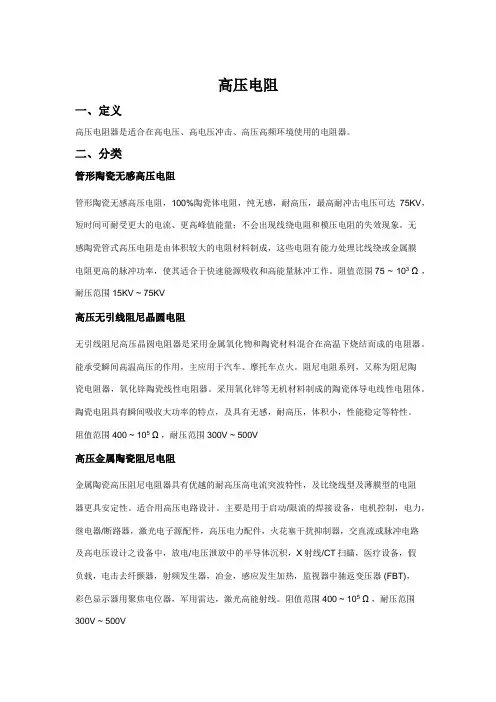
高压电阻一、定义高压电阻器是适合在高电压、高电压冲击、高压高频环境使用的电阻器。
二、分类管形陶瓷无感高压电阻管形陶瓷无感高压电阻,100%陶瓷体电阻,纯无感,耐高压,最高耐冲击电压可达75KV,短时间可耐受更大的电流、更高峰值能量;不会出现线绕电阻和模压电阻的失效现象。
无感陶瓷管式高压电阻是由体积较大的电阻材料制成,这些电阻有能力处理比线绕或金属膜电阻更高的脉冲功率,使其适合于快速能源吸收和高能量脉冲工作。
阻值范围75 ~ 103Ω,耐压范围15KV ~ 75KV高压无引线阻尼晶圆电阻无引线阻尼高压晶圆电阻器是采用金属氧化物和陶瓷材料混合在高温下烧结而成的电阻器。
能承受瞬间高温高压的作用,主应用于汽车、摩托车点火。
阻尼电阻系列,又称为阻尼陶瓷电阻器,氧化锌陶瓷线性电阻器。
采用氧化锌等无机材料制成的陶瓷体导电线性电阻体。
陶瓷电阻具有瞬间吸收大功率的特点,及具有无感,耐高压,体积小,性能稳定等特性。
阻值范围400 ~ 105Ω,耐压范围300V ~ 500V高压金属陶瓷阻尼电阻金属陶瓷高压阻尼电阻器具有优越的耐高压高电流突波特性,及比绕线型及薄膜型的电阻器更具安定性。
适合用高压电路设计。
主要是用于启动/限流的焊接设备,电机控制,电力,继电器/断路器,激光电子源配件,高压电力配件,火花塞干扰抑制器,交直流或脉冲电路及高电压设计之设备中,放电/电压泄放中的半导体沉积,X射线/CT扫瞄,医疗设备,假负载,电击去纤颤器,射频发生器,冶金,感应发生加热,监视器中驰返变压器 (FBT),彩色显示器用聚焦电位器,军用雷达,激光高能射线。
阻值范围400 ~ 105Ω,耐压范围300V ~ 500V氧化膜高压高频电阻氧化膜高压高频电阻器采用管形端头被银或金电极结构,主要用作超高频电路中的负载。
阻值范围50 ~ 75 Ω,耐压范围3.2KV ~ 12.5KV棒状高压玻璃釉膜电阻棒状高压玻璃釉膜电阻器,主要是用於交直流或脉冲电路及高压设备中。
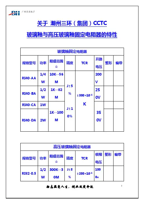
关于潮州三环(集团)CCTC玻璃釉与高压玻璃釉固定电阻器的特性玻璃釉固定电阻器规格型号功率阻值范围Ω精度TCR开路电压整形编带RI40-AA 1/4W 10K--56MJ±5%J±1 0% ±350×10-6K200VRI40-BA 1/2W 1K--82M250V RI40-CA 1W1K--100M350V RI40-DA 2W高压玻璃釉固定电阻器规格型号功率阻值范围Ω精度TCR极限电压整形编带RI82-0.5 1/2W 300K--30M J±5%J±10%±250×10-6K1500vRI82-1 1W 3000 v1、玻璃釉固定电阻器RI40产品特性:1、具有过负荷延时熔断功能。
2、阻燃型结构、安全性能高。
3、小尺寸,可节省安装空间。
4、适用于安规要求,通过CQC认证。
5、采用色码标志。
2、高压玻璃釉电阻器RI82产品特性:1、耐高温、耐高温、耐湿特性优良。
2、应用于高压隔离或高压放电电路中。
3、采用色码标志。
4、适用于安规要求通过UL认证、TUV认证、CQC认证。
问题:1、玻璃釉电阻器生产和应用方面上的问题,想深化了解下。
2、?附:网站上查阅到玻璃釉电阻器的相关资料:1、玻璃釉电阻由贵金属银钯、钌、铑等的金属氧化物(氧化钯、氧化钌等)和和玻璃釉黏合剂混合成浆料,涂覆在绝缘骨架上,经高温烧结而成。
此电阻阻值范围宽,价廉,温度系数小,耐湿性好,此种电阻器又称厚膜电阻器。
2、CQC认证中国质量认证中心(英文缩写CQC)。
CQC是代表中国加入国际电工委员会电工产品合格测试与认证组织(IECEE)多边互认(CB)体系的国家认证机构(NCB),是加入国际认证联盟(IQNet)和国际有机农业运动联盟(IFOAM)的国家认证机构,CQC与国外诸多知名认证机构间的国际互认业务,以及广泛的国际交流,使CQC赢得了良好的国际形象。
一、概述1. 介绍玻璃釉瞙固定电阻器的概念和作用;2. 引出本文重点探讨的主题——ri80型玻璃釉瞙固定电阻器的比热容。
二、 ri80型玻璃釉瞙固定电阻器的基本结构与性能1. ri80型玻璃釉瞙固定电阻器的结构;2. ri80型玻璃釉瞙固定电阻器的特性与性能。
三、比热容的概念及其在固定电阻器中的作用分析1. 比热容的定义和意义;2. 比热容在固定电阻器中的作用及重要性。
四、理论计算与实际测量1. ri80型玻璃釉瞙固定电阻器比热容的理论计算方法;2. ri80型玻璃釉瞙固定电阻器比热容的实际测量过程和结果分析。
五、比热容对固定电阻器性能的影响1. 比热容对电阻器的稳定性和精度的影响;2. 比热容对电阻器的温度特性和使用寿命的影响。
六、提高ri80型玻璃釉瞙固定电阻器比热容的途径与措施1. 提高电阻材料的比热容;2. 优化固定电阻器的结构设计。
七、结论1. 总结ri80型玻璃釉瞙固定电阻器比热容的研究成果;2. 展望未来固定电阻器比热容研究的发展方向。
八、比热容的概念及其在固定电阻器中的作用分析比热容是指物质单位质量在温度变化时吸收或放出的热量的大小,通常用符号C表示。
在固定电阻器中,比热容的重要性不言而喻。
电阻器在工作过程中会受到外部环境温度的影响,而比热容的大小决定了电阻器对温度变化的响应能力。
一般来说,比热容越大,电阻器在受到热量影响时温度变化越缓慢,稳定性越好。
比热容是影响固定电阻器稳定性和性能的重要因素之一。
在固定电阻器中,因为电阻器的主体结构是由电阻材料和外部封装材料组成的,在温度变化时,这些材料会受到热胀冷缩的影响,从而导致电阻值发生变化。
而比热容就是在描述材料在温度变化时对热量的反应能力,从而影响了电阻值的稳定性。
了解并研究固定电阻器材料的比热容特性,既有助于改善固定电阻器的温度特性,也有助于提高电阻器的稳定性和精度。
在实际应用中,通过研究固定电阻器材料的比热容特性,可以为固定电阻器的设计和生产提供重要的参考依据。
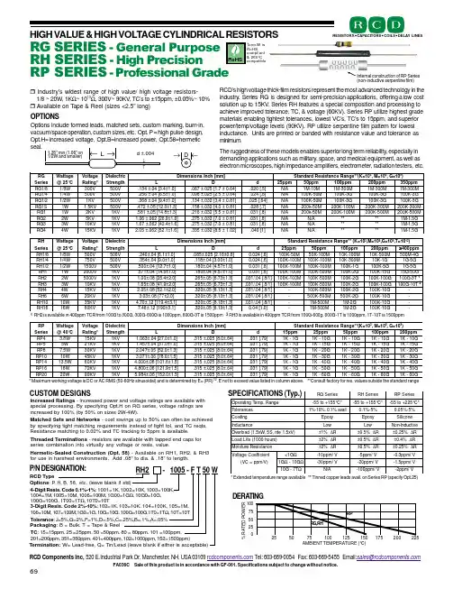
Internal construction of RP Series (non-inductive serpentine film)U U U U UU U U U UIndustry’s widest range of high value/ high voltage resistors- 1/8 ~ 20W, 1K Ω~ 1013Ω, 300V~ 90KV , TC’s to ±15ppm, ±0.05%~ 10% Available on T ape & Reel (sizes <2.5” long)RCD’s high voltage thick-film resistors represent the most advanced technology in the industry. Series RG is designed for semi-precision applications, offering a low cost solution up to 15KV . Series RH features a special composition and processing to achieve improved tolerance, TC, & voltage (60KV). Series RP utilize highest grade materials enabling tightest tolerances, lowest VC’s, TC’s to 15ppm, and superior power/temp/voltage levels (90KV). RP utilize serpentine film pattern for lowest inductance. Units are printed or banded with resistance value and tolerance as minimum.The ruggedness of these models enables superior long term reliability, especially in demanding applications such as military, space, and medical equipment, as well as electron microscopes, high impedance amplifiers, electrometer, radiation testers, etc.* Maximum working voltage is DC or AC RMS (50-60Hz sinusoidal) and is determined by E= (PR)1/2, E not to exceed value listed in column above. **Consult factory for res. values outside the standard rangeOPTIONSOptions include formed leads, matched sets, custom marking, burn-in,vacuum/space operation, custom sizes, etc. Opt. P = high pulse design,Opt.H= increased voltage, Opt.B=increased power, Opt.58=hermetic seal.* Extended temperature range available ** Tinned copper leads avail. on Series RP (specify Opt.25)DERA TING100 75 50 25 025 50 75 100 125 150 175 200 225AMBIENT TEMPERATURE (°C)% R A T E D P O W E RRPRG,RHIncreased Ratings - increased power and voltage ratings are available with special processing. By specifying Opt.H on RG series, voltage ratings are increased by 100% (by 50% on sizes 2W-4W).Matched Sets and Networks - cost savings up to 50% can often be achieved by specifying tight matching requirements instead of tight tol. and TC reqts.Resistance matching to 0.02% and TC tracking to 5ppm is available.Threaded Terminations - resistors are available with tapped end caps for series combination into virtually any voltage or resis. value.Hermetic-Sealed Construction (Opt. 58) - Available on RH1, RH2, & RH3for use in harshest environments. Add .08” to dia. & .18” to length.CUSTOM DESIGNS SPECIFICATIONS (Typ.)1RH2 is available in 400ppm TCR from 100G to 300G, 300G-600G is 1000ppm, 600G-3T is 1500ppm 2 RH3 is available in 400ppm TCR from 100G-600g, 600G-1T is 1000ppm, 1T-10T is 1500ppmG R W e g a t t a e g a tl o V c i r t c e l e i D ]m m [h c n I s n o i s n e m i D 01=K (**e g n a R e c n a ts i s e R d r a d n a t S 301=M ,601=G ,9)s e i r e S C °52@*g n i t a R h t g n e r t S L Dd m pp 52m p p 05mp p 001m p p 002m p p 0538/1G R W 8/1V 003V 005]0.1±4.3[40.±431.]46.0±7.1[520.±760.]5.[020.A /N M 01-M 1M 003-M 1M 003-M 1M 003-M 14/1G R W 4/1V 005V 005]0.1±5.6[40.±652.]46.0±5.2[520.±890.]6.[420.A /N M 05-K 001G 3-K 001G 3-K 001G 3-K 0012/1G R W 2/1V K 1V 005]0.1±4.9[40.±863.]18.0±4.3[230.±431.]46.[520.A /N M 05-K 001G 3-K 001G 3-K 001G 3-K 001S 1G R W 1V K 5.1V 005]3.1±0.21[50.±274.]18.0±0.4[230.±851.]7.[820.A /N M 05-k 002M 001-K 002M 003-K 002M 003-K 0021G R W 1V K 2V K 1]3.1±8.41[50.±185.]18.0±5.5[230.±612.}8.[130.A /N M 05-k 002M 001-K 002M 005-K 002M 005-K 0022G R W 2V K 5V K 1]6.1±9.62[260.±60.1]18.0±0.7[230.±572.}8.[130.A /N A /N ****G 5.1-M 13G R W 3V K 01V K 1]6.1±4.24[260.±76.1]18.0±0.7[230.±572.}8.[130.A /N A /N ****G 5.1-M 14G R W4VK 51VK 1]6.1±1.25[260.±50.2]20.1±5.8[230.±533.]1[040.A /N A /N ****G5.1-M 1P R W e g a t t a e g a t l o V c i r t c e l e i D ]m m [h c n I s n o i s n e m i D 01=K (**e g n a R e c n a t s i s e R d r a d n a t S 301=M ,601=G ,9)s e i r e S C °04@*g n i t a R h t g n e r t S L D d m p p 51m p p 52m p p 05m p p 001m p p 0024P R W 8.3V K 51V K 1]0.1±0.72[40.±360.1]46.±0.8[520.±513.]97.[130.G 1-K 1G 01-K 1G 01-K 1G 01-K 1G 01-K 15P R W 5V K 12V K 1]0.1±0.73[40.±754.1]46.±0.8[520.±513.]97.[130.G 1-K 1G 51-K 1G 51-K 1G 51-K 1G 51-K 18P R W 5.7V K 03V K 1]3.1±0.25[50.±740.2]46.±0.8[520.±513.]97.[130.G 1-K 1G 02-K 1G 02-K 1G 02-K 1G 02-K 101P R W 01V K 54V K 1]5.1±0.87[60.±170.3]46.±0.8[520.±513.]97.[130.G 1-K 1G 03-K 1G 03-K 1G 03-K 1G 03-K 11P R 4W 5.31V K 06V K 1]5.1±6.101[60.±000.4]46.±0.8[520.±513.]97.[130.G 1-K 1G 04-K 1G 04-K 1G 04-K 1G 04-K 161P R W 61V K 27V K 1]5.1±9.121[60.±008.4]46.±0.8[520.±513.]97.[130.G 1-K 1G 05-K 1G 05-K 1G 05-K 1G 05-K 102P R W 02V K 09V K 1]5.1±0.251[60.±489.5]46.±0.8[520.±513.]97.[130.G 1-K 1G 06-K 1G 06-K 1G 06-K 1G06-K 1s e i r e S G R s e i r e S H R s e i r e S P R e g n a R .p m e T g n i t a r e p O *C °551+o t 55-*C °551+o t 55-*C °522+o t 55-s e c n a r e l o T li a v a %1.0,%01-%1%5-%1.0%5-%50.0g n i t a o C y x o p E y x o p E e n o c i l i S ec n a t c ud n I w o L w o Le v i t c u d n I -n o N )V x 5.1e t n ,S 5,W x 5.1(d a o l r e v O %1±∆R %5.0±∆R %52.0±∆R )s r u o h 0001(ef i L d a o L %2±∆R %5.0±∆R %4.0±∆R e c n a t s i s e R e r u t s i o M %2±∆R %5.0±∆R %52.0±∆R tn e i c i f f e o C e g a t l o V G 1<ΩV /m p p 01-V /m p p 5-V /m p p 3.0-)V /m p p =C V (G 1ΩG 01-ΩV/m p p 03-V /m p p 02-V /m p p 5.1-T 7-G 01ΩA/N V/m p p 001-V/m p p 2-HR W e g a t t a e g a t l o V c i r t c e l e i D ]m m [h c n I s n o i s n e m i D 01=K (**e g n a R e c n a t s i s e R d r a d n a t S 301=M ,601=G ,901=T ,21)s e i r e S C °52@*g n i t a R h t g n e r t S L Ddm p p 52m p p 05m p p 001m p p 002≥m p p 0048/1H R W 8/1V 005V 005]0.1±1.6[40.±042.]6.0±61.2[520.±580.]6.[420.0M 05-K 001M 001-K 05M 001-K 01M 005-K 01G 4-M 0054/1H R W 4/1V 057V 005]0.1±0.9[40.±453.]0.1±00.3[40.±811.]6.[420.0M 001-K 001M 001-K 001M 003-K 01G 1-K 01G 5-G 12/1H R W 2/1V 0051V 005]0.1±7.21[40.±005.]0.1±75.4[40.±081.]8.[130.0M 001-K 001M 001-K 001G 1-K 001G 5-K 001G 5-G 11H R W 1V 0002V K 1]0.1±5.41[40.±175.]0.1±75.4[40.±081.]8.[130.0M 001-K 001M 005-K 001G 2-K 001G 51-K 001G 05-G 512H R W 2V 0005V K 1]0.2±4.52[80.±00.1]3.1±37.6[50.±562.]1/8.[40./130.M 001-K 001M 005-K 001G 2-K 001G 001-K 001T 3-G 00113H R W 3V K 01V K 1]0.2±9.14[80.±56.1]3.1±37.6[50.±562.]1/8.[40./130.M 001-K 001M 005-K 001G 2-K 001G 001-K 001T 01-G 00124H R W 4V K 51V K 1]0.2±1.25[80.±50.2]3.1±31.8[50.±023.]1/8.[40./130.-M 005-K 001G 2-K 001G 01-K 001-6H R W 6V K 02V K 1]0.2±77[80.±30.3]3.1±31.8[50.±023.]1/8.[40./130.-M 005-K 005G 2-K 005G 01-K 001-01H R W 01V K 53V K 1]1.3±4.911[21.±07.4]3.1±31.8[50.±023.]1/8.[40./130.-M 005-M 1G 2-M 1G 01-K 001-61H R W 61V K 06V K 1]1.3±091[21.±84.7]3.1±31.8[50.±023.]0.1[40.0-M 005-M 1G 2-M 1G 01-K 001-FA036C Sale of this product is in accordance with GF-061. Specifications subject to change without notice.RCD Components Inc, 520 E.Industrial Park Dr, Manchester, NH, USA 03109 Tel: 603-669-0054 Fax: 603-669-5455 Email:***********************RESISTORS CAPACITOR S C OILS DELAY LINESHIGH VALUE & HIGH VOLT AGE CYLINDRICAL RESISTORSRG SERIES - General Purpose RH SERIES - High PrecisionRP SERIES - Professional Grade69TC RCD Type1004=1M , Packaging Tolerance Options : P , Term.W is RoHS compliant & 260°C compatible。

高压玻璃釉膜电阻器1.引言1.1 概述概述高压玻璃釉膜电阻器是一种常见的电子元件,用于阻碍电流的流动。
它由一层玻璃釉膜覆盖在陶瓷基片上,并通过电极连接到电路中。
高压玻璃釉膜电阻器具有高阻值、稳定性好、电压承受能力强等特点,在电子设备和电路中有广泛的应用。
本文将介绍高压玻璃釉膜电阻器的定义和特点,并探讨其在各个领域的应用。
同时,通过总结高压玻璃釉膜电阻器的重要性和优势,展望其未来的发展前景。
在接下来的章节中,我们将详细介绍高压玻璃釉膜电阻器的定义、结构、工作原理和特点。
同时,我们还将深入探讨高压玻璃釉膜电阻器在通信、电力、医疗等领域的应用案例,并讨论其在这些领域中的重要性和优势。
最后,我们将对高压玻璃釉膜电阻器的重要性和优势进行总结,并展望其未来的发展前景。
我们认为,随着电子技术的不断进步和应用领域的不断拓展,高压玻璃釉膜电阻器将会发挥更加重要的作用,并在技术和市场上取得更大的突破。
希望通过本文的介绍和分析,读者能够对高压玻璃釉膜电阻器有更深入的了解,并认识到其在电子领域中的重要性和潜力。
同时,也希望本文能够为相关研究人员和从业人员提供一些参考和借鉴,促进高压玻璃釉膜电阻器的进一步发展和应用。
1.2 文章结构文章结构是指整篇文章的框架和组织方式,通过明确的结构可以使读者更好地理解文章的逻辑关系和主旨。
本文以“高压玻璃釉膜电阻器”为主题,主要分为引言、正文和结论三个部分。
引言部分首先对文章进行概述,简要介绍高压玻璃釉膜电阻器的基本概念和意义。
接着,介绍文章的结构,即可以明确说明本文包括哪些内容,帮助读者在阅读时有一个整体的认识。
正文部分是全文的主体部分,包含两个小节。
首先,2.1节主要定义高压玻璃釉膜电阻器并阐述其特点,介绍其结构、原理以及一些相关的技术参数。
然后,在2.2节中,探讨高压玻璃釉膜电阻器的应用领域,包括但不限于电力系统、电子设备、通信网络等方面,以及其在这些领域中的具体应用案例。
结论部分对文章进行总结,并展望高压玻璃釉膜电阻器的发展前景。
玻璃釉电阻的温漂-概述说明以及解释1.引言1.1 概述玻璃釉电阻是一种电子元件,其釉层是由玻璃釉材料制成的。
它具有良好的绝缘性能和较高的耐磨损性,因此被广泛应用于电子设备中。
然而,随着温度的变化,玻璃釉电阻的电阻值也会发生变化,这就是所谓的温漂现象。
温漂是指在温度变化过程中,物体的某些性质或参数发生变化的现象。
对于玻璃釉电阻而言,温漂主要表现为电阻值随着温度的升高或降低而发生变化。
这种温漂现象对于一些需要精确控制的电路设计和工程应用来说是一个重要的考虑因素。
如果温漂现象被忽视或未能有效地加以控制,可能会导致电路性能的不稳定或失效。
为了解决温漂问题,科学家和工程师们提出了一些解决方法。
其中一种常见的方法是采用温度补偿电路,通过引入补偿元件或采用特殊的电路设计来抵消温漂效应。
此外,选择合适的材料和制造工艺也能有效地减小温漂现象。
综上所述,了解和控制玻璃釉电阻的温漂现象对于电子设备的正常运行和性能稳定具有重要意义。
在实际应用中,必须认真考虑和研究温漂现象,并采取相应的措施来减小温漂对玻璃釉电阻的影响,以确保电路的可靠性和稳定性。
1.2 文章结构本文将从以下几个方面对玻璃釉电阻的温漂现象进行深入研究和探讨。
首先,我们将介绍玻璃釉电阻的定义和原理,包括其基本构造和工作原理。
接着,我们将详细讨论玻璃釉电阻在温度变化下的温漂现象,探究其产生的原因和机制。
此外,我们还将分析温漂对玻璃釉电阻性能的影响,如电阻值的变化和稳定性的下降等。
最后,我们将提出可能的解决方法,包括优化设计和材料选择等,以减小温漂对玻璃釉电阻的影响。
通过对玻璃釉电阻的温漂现象进行深入研究,本文旨在提高对该现象的理解,并为相关领域的研究和应用提供参考和指导。
1.3 目的本文的目的是对玻璃釉电阻的温漂现象进行深入研究和分析,以了解温度变化对玻璃釉电阻特性的影响。
通过对玻璃釉电阻的定义和原理进行介绍,进一步探讨温漂现象的成因和机理,以及温漂对玻璃釉电阻性能的影响。
高压玻璃釉分压电阻
从材料角度来看,高压玻璃釉分压电阻通常采用特殊的陶瓷材料或玻璃材料制成,以确保在高压下具有良好的绝缘性能和耐压能力。
这些材料通常具有较高的介电常数和绝缘强度,能够在高压环境下稳定地工作。
从电气特性角度来看,高压玻璃釉分压电阻通常具有较高的分压比和准确的分压系数,以确保在高压下提供稳定的分压功能。
此外,它们通常具有较低的温度系数和较高的耐压能力,以适应各种恶劣的工作环境。
总的来说,高压玻璃釉分压电阻在电力系统中起着至关重要的作用,它们能够确保高压电路中的电压能够被有效地分压到需要的电压级别,从而保证电力系统的安全稳定运行。