完整版TEM高分辨透射电镜讲稿
- 格式:ppt
- 大小:5.72 MB
- 文档页数:58
1.Brief introductionTransmission electron microscopyTransmission electron microscopy (TEM) is a microscopy technique in which a beam of electrons is transmitted through an ultra-thin specimen, interacting with the specimen as it passes through it. An image is formed from the interaction of the electrons transmitted through the specimen; the image is magnified and focused onto an imaging device, such as a fluorescent screen, on a layer of photographic film, or to be detected by a sensor such as a CCD camera.2.Development:The first TEM was built by Max Knoll and Ernst Ruska in 1931, with this group developing the first TEM with resolution greater than that of light in 1933. The first commercial TEM was produced by Siemens AG of Germany in 1939. In 1986, Ruska was awarded the Nobel Prize in physics for the development of transmission electron microscopy.ponents:A TEM is composed of several components (Vacuum system 、Specimen stage、Electron gun、Electron lens、Apertures,)which include a vacuum system in which the electrons travel, an electron emission source for generation of the electron stream, a series of electromagnetic lenses, as well as electrostatic plates. The latter two allow the operator to guide and manipulate the beam as required. Also required is a device to allow the insertion into, motion within, and removal of specimens from the beam path. Imaging devices are subsequently used to create an image from the electrons that exit the system.Vacuum systemTo increase the mean free path of the electron gas interaction, a standard TEM is evacuated to low pressures, typically on the order of 10−4 Pa. The need for this is twofold: first the allowance for the voltage difference between the cathode and the ground without generating an arc, and secondly to reduce the collision frequency of electrons with gas atoms to negligible levels—this effect is characterized by the mean free path.Specimen stageThe specimen holders are adapted to hold a standard size of grid upon which the sample is placed or a standard size of self-supporting specimen. Standard TEM grid sizes are a 3.05 mm diameter ring, with a thickness and mesh size ranging from a few to 100 μm. The sample is placed onto the inner meshed area having diameter of approximately 2.5 mm. Usual grid materials are copper, molybdenum, gold or platinum.Electron gunBy connecting the filament to the negative component power supply, electrons can be "pumped" from the electron gun to the anode plate, and TEM column, thus completing the circuit. The gun is designed to create a beam of electrons exiting fromthe assembly at some given angle, known as the gun divergence semi-angle, α. By constructing the Wehnelt cylinder such that it has a higher negative charge than the filament itself, electrons that exit the filament in a diverging manner are, under proper operation, forced into a converging pattern the minimum size of which is the gun crossover diameter.Electron lens4.Application:TEMs are capable of imaging at a significantly higher resolution than light microscopes, owing to the small de Broglie wavelength of electrons. This enables the instrument's user to examine fine detail—even as small as a single column of atoms, which is thousands of times smaller than the smallest resolvable object in a light microscope. TEM forms a major analysis method in a range of scientific fields, in both physical and biological sciences. TEMs find application in cancer research, virology, materials science as well as pollution, nanotechnology, and semiconductor research. Ernst Abbe originally proposed that the ability to resolve detail in an object was limited approximately by the wavelength of the light used in imaging, which limits the resolution of an optical microscope to a few hundred nanometers. Developments into ultraviolet (UV) microscopes, led by Köhler and Rohr, allowed for an increase in resolving power of about a factor of two. However this required more expensive quartz optical components, due to the absorption of UV by glass. At this point it was believed that obtaining an image with sub-micrometer information was simply impossible due to this wavelength constraint.5.formation theory:Contrast formation in the TEM depends greatly on the mode of operation. Complex imaging techniques, which utilize the unique ability to change lens strength or to deactivate a lens, allow for many operating modes. These modes may be used to discern information that is of particular interest to the investigator.(1)Bright field:吸收像The most common mode of operation for a TEM is the bright field imaging mode. In this mode the contrast formation, when considered classically, is formed directly by occlusion and absorption of electrons in the sample. Thicker regions of the sample, or regions with a higher atomic number will appear dark, while regions with no sample in the beam path will appear bright –hence the term "bright field". The image is in effect assumed to be a simple two dimensional projection of the sample down the optic axis, and to a first approximation may be modeled via Beer's law, more complex analyses require the modeling of the sample to include phase information.(2)Diffraction contrast衍射像Transmission electron micrograph of dislocations in steel, which are faults in the structure of the crystal lattice at the atomic scaleSamples can exhibit diffraction contrast, whereby the electron beam undergoesBragg scattering, which in the case of a crystalline sample, disperses electrons into discrete locations in the back focal plane. By the placement of apertures in the back focal plane, i.e. the objective aperture, the desired Bragg reflections can be selected (or excluded), thus only parts of the sample that are causing the electrons to scatter to the selected reflections will end up projected onto the imaging apparatus.(3)Phase contrast相位像Crystal structure can also be investigated by high-resolution transmission electron microscopy (HRTEM), also known as phase contrast. When utilizing a Field emission source and a specimen of uniform thickness, the images are formed due to differences in phase of electron waves, which is caused by specimen interaction.[31] Image formation is given by the complex modulus of the incoming electron beams. As such, the image is not only dependent on the number of electrons hitting the screen, making direct interpretation of phase contrast images more complex. However this effect can be used to an advantage, as it can be manipulated to provide more information about the sample, such as in complex phase retrieval techniques.透射电镜技术在好氧污泥颗粒超微结构研究中的应用_刘晓云.pdf。


TEM透射电镜中的电子衍射及分析TEM透射电镜(Transmission Electron Microscopy)是一种高分辨率的显微镜,它利用电子束穿透样品,并通过电子衍射和显微成像技术来观察样品的内部结构和晶格信息。
本文将通过一个实例来介绍TEM透射电镜中的电子衍射及分析过程。
实例:研究纳米材料的晶格结构研究目标:使用TEM透射电镜研究一种纳米材料的晶格结构,确定其晶格常数和晶体结构。
实验步骤:1.样品制备:首先,需要制备纳米材料的TEM样品。
常见的制备方法包括溅射,化学气相沉积和溶液法等。
在本实验中,我们将使用溶液法制备纳米颗粒样品,并将其沉积在碳膜上。
2.装载样品:将TEM样品加载到TEM透射电镜的样品台上,并进行适当的调整,以使样品位于电子束的路径中。
3.调整TEM参数:调整透射电镜的参数,如电子束的亮度,聚焦和对比度等。
这些参数的调整对于获得良好的电子衍射图像至关重要。
4. 获得电子衍射图:通过调整TEM中的衍射镜,观察和记录电子衍射图。
可以使用选区衍射(Selected Area Diffraction,SAD)模式,在样品上选择一个小区域进行衍射。
电子束通过纳米颗粒样品时,会与晶体的原子排列相互作用,并在相应的探测器上形成衍射斑图。
5.解析电子衍射图:利用电子衍射图分析软件,对获得的电子衍射图进行解析。
通过测量衍射斑的位置和相对强度,可以推断出样品的晶格常数和晶体结构。
6.确定晶格常数:根据衍射斑的位置,使用布拉格方程计算晶格常数。
布拉格方程为:nλ = 2dsin(θ)其中,n是衍射阶数,λ是电子波长,d是晶体平面的间距,θ是入射角。
通过测量不同衍射斑的位置和计算,可以得到晶格常数及其误差范围。
7.确定晶体结构:根据衍射斑的相对强度以及已知的晶格常数,可以利用衍射斑的几何关系推断样品的晶体结构。
常见的晶体结构包括立方晶系、六方晶系等。
8.结果分析:根据实验获得的数据,进行晶格常数和晶体结构的分析和比较。

![[指南]TEM透射电镜](https://uimg.taocdn.com/af4d958e50e79b89680203d8ce2f0066f5336403.webp)
透射电子显微镜实验目的1. 掌握透射电镜的工作原理和基本结构2. 了解和掌握透射电镜的样品前处理及数据后处理过程3. 了解透射电镜的操作方法实验原理根据阿贝成像原理,更短波长的光源才能得到更高分辨率的图像;而由波粒二象性可以知道,高速运动的电子波长非常短。
透射电镜就是利用磁场对电子进行聚焦,聚焦后的电子束与样品相互作用,从而得到高分辨的样品形貌。
图1 透射电镜的成像原理透射电镜的成像主要分为两个过程:一是平等电子束与样品作用产生衍射束经磁透镜聚集后形成各级衍射谱,即样品的结构信息通过衍射谱呈现出来;二是从各级衍射谱发出的相干波通过干涉重新在像平面上形成反映样品形貌特征的像。
显然从试样同一点发出的各级衍射波经过上述两个过程后在像平面上会聚集为一点,而从试样不同点发出的同级衍射波经过透镜后,都会聚集到后焦面上的一点。
当中间镜的物平面与物镜的像平面重合时,得到三级高倍放大像,即试样显微成像;当中间镜的位置与物镜的背焦面重合时,将得到放大了的衍射谱,即衍射花样成像。
当成像方式为显微成像时,总的透射电镜总的放大倍数就是各个透镜倍率的乘积。
而改变中间镜的电流,调节其焦距使得中间镜物平面移到物镜的后焦面,便可在屏上看到像的后焦面以及变换成衍射谱的过程。
用物镜光阑选择物镜后焦面上的不同衍射斑点,并使所选电子束成像就可以获得不同模式的像。
选择透射波时,观察到的是明场像;选择衍射波时,观察到的是暗场像;当后焦面上的物镜光阑尺寸较大时,可以使两个以上的波干涉成像,观察到的是高分辨电子显微像。
高分辨像主要有晶格条纹像,一维结构像,二维晶格像,二维结构像和特殊像五类。
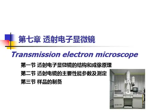
透射电镜主要由电子光学系统、真空系统和电子控制系统等部分组成,其中电子光学系统是决定透射电镜性能最关键的部分。
另外,有些透射电镜还配置有X射线能谱、电子能量损失谱等附件。
电子光学系统由照明系统、成像系统和图像观察记录系统组成。
照明系统由电子枪和几个电磁聚光镜组构成,主要是提供一个亮度高、尺寸小、性能稳定的光源。