12pF贴片电容0603CG120J500NT《风华电容样品单》
- 格式:pdf
- 大小:1.16 MB
- 文档页数:3
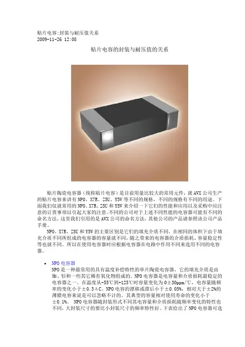
贴片电容:封装与耐压值关系2009-11-26 12:08贴片电容的封装与耐压值的关系贴片陶瓷电容器(统称贴片电容)是目前用量比较大的常用元件,就AVX公司生产的贴片电容来讲有NPO、X7R、Z5U、Y5V等不同的规格,不同的规格有不同的用途。
下面我们仅就常用的NPO、X7R、Z5U和Y5V来介绍一下它们的性能和应用以及采购中应注意的订货事项以引起大家的注意。
不同的公司对于上述不同性能的电容器可能有不同的命名方法,这里我们引用的是AVX公司的命名方法,其他公司的产品请参照该公司产品手册。
NPO、X7R、Z5U和Y5V的主要区别是它们的填充介质不同。
在相同的体积下由于填充介质不同所组成的电容器的容量就不同,随之带来的电容器的介质损耗、容量稳定性等也就不同。
所以在使用电容器时应根据电容器在电路中作用不同来选用不同的电容器。
•NPO电容器NPO是一种最常用的具有温度补偿特性的单片陶瓷电容器。
它的填充介质是由铷、钐和一些其它稀有氧化物组成的。
NPO电容器是电容量和介质损耗最稳定的电容器之一。
在温度从-55℃到+125℃时容量变化为0±30ppm/℃,电容量随频率的变化小于±0.3ΔC。
NPO电容的漂移或滞后小于±0.05%,相对大于±2%的薄膜电容来说是可以忽略不计的。
其典型的容量相对使用寿命的变化小于±0.1%。
NPO电容器随封装形式不同其电容量和介质损耗随频率变化的特性也不同,大封装尺寸的要比小封装尺寸的频率特性好。
下表给出了NPO电容器可选取的容量范围:NPO电容器适合用于振荡器、谐振器的槽路电容,以及高频电路中的耦合电容。
•X7R电容器X7R电容器被称为温度稳定型的陶瓷电容器。
当温度在-55℃到+125℃时其容量变化为15%,需要注意的是此时电容器容量变化是非线性的。
X7R电容器的容量在不同的电压和频率条件下是不同的,它也随时间的变化而变化,大约每10年变化1%ΔC,表现为10年变化了约5%。
广东风华高新科技股份有限公司GUANGDONG FENGHUA ADV ANCED TECHNOLOGY HOLDING CO.,LTD.承认书APPROV AL SHEET客户名称:CUSTOMER品名:常规厚膜片式固定电阻器PARTNAME规格版本号VERSION日期DATE制造客户APPROV AL APPROV AL 拟制审核确认检验审核批准FENGHUAFENG HUA ADV ANCED TECHNOLOGY (HOLDING) CO., LTD序号 No 目 录TABLE OF CONTENTS1.0 概述Summary2.0 结构及尺寸Structure And Dimensions3.0 型号规格表示办法How To Order4.0 电气性能Performance Specification5.0 可靠性Reliability Data6.0 包装Package7.0 环保情况说明 Environmental Protection Statement 8.0 推荐使用的焊接曲线Recommended soldering profile 9.0 使用注意事项Precautions For UseRC/RS□□□□1.0概述Summary片式电阻器主要生产的型号包括01005、0201、0402、0603、0805、1206、1210、2010、2512。
其特点是:The dimension type for chip resistor including01005、 0201、0402、0603、0805、1206、1210、2010、2512, and the features are as below:*体积小、重量轻miniature and light weight*电性能稳定,可靠性高 stable electrical capability and high reliability *机械强度高、高频特性优越superior mechanical and frequency*装配成本低,并与自动贴装设备匹配low assembly cost, suit for automatic SMT *适应再流焊与波峰焊suit for re-flow and wave flow soldering .*符合ROHS指令要求Compliant with ROHS Directive*符合无卤素要求Compliant with halogen free requirement*禁止使用SS-00259中规定的1级环境管理物质*SONY指定原材料只能从绿色伙伴认定供应商处采购产品广泛应用于计算机、通讯、工业自动化、航天航空、军事、数字电视、数字音响及消费类电子等领域。
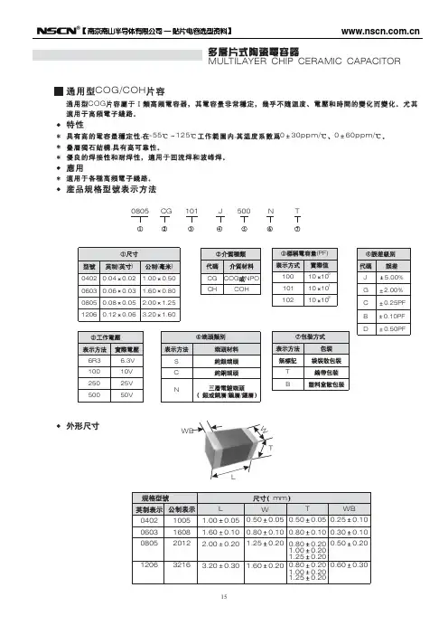
【 南京南山半导体有限公司 — 贴片电容选型资料】MULTILAYER CHIP CERAMIC CAPACITORCOG/COHCOG, ,-55125,030ppm/060ppm/0805CG101J500NT(PF) ( 0402 0.04 0603 0.06 0805 0.08 1206 0.12 ) 0.02 0.03 0.05 0.06 1.00 1.60 2.00 3.20 ( ) 0.50 0.80 1.25 1.60 CG CH COG NPO COH 100 101 102 10 100 1J G C B D5.00% 2.00% 0.25PF 0.10PF 0.50PF10 10 10 1026R3 100 250 5006.3V 10V 25V 50VS C N / / T BWBWTL mm L 0402 0603 0805 1206 1005 1608 2012 3216 1.00 1.60 2.00 3.20 0.05 0.10 0.20 0.30 W 0.50 0.80 1.25 1.60 0.05 0.50 0.10 0.80 0.20 0.80 1.00 1.25 0.20 0.80 1.00 1.25 T WB 0.05 0.25 0.10 0.30 0.20 0.50 0.20 0.20 0.20 0.60 0.20 0.20 0.10 0.10 0.20 0.3015【 南京南山半导体有限公司 — 贴片电容选型资料】0.80 0.20 1.00 0.20 0.50 0.80 0.20 1.00 0.20 0.600.20 0.30【 南京南山半导体有限公司 — 贴片电容选型资料】MULTILAYER CHIP CERAMIC CAPACITORCOG/COH 0402 0603 0805 12066.3V 10V 16V 25V 50V 6.3V 10V 16V 25V 50V 6.3V 10V 16V 25V 50V 6.3V 10V 16V 25V 50V0.5PF 1PF 2PF 3PF 4PF 5PF 6PF 7PF 10PF 22PF 33PF 47PF 68PF 100PF 120PF 150PF 180PF 220PF 330PF 470PF 560PF 680PF 1000PF 2200PF 2700PF 3300PF 4700PF 5600PF 6800PF 10nF 12nF 15nF 22nF 47nF 68nF 100nF17【 南京南山半导体有限公司 — 贴片电容选型资料】04020603080512066.3V 10V 16V 25V 50V 6.3V 10V 16V 25V 50V 6.3V 10V 16V 25V 50V 6.3V 10V 16V 25V 50VCapacitance0.5PF 1PF 2PF 3PF 4PF 5PF 6PF 7PF 10PF 22PF 33PF 47PF 68PF 100PF 120PF 150PF 180PF 220PF 330PF 470PF 560PF 680PF 1000PF 2200PF 2700PF 3300PF 4700PF 5600PF 6800PF 10nF 12nF 15nF 22nF 47nF 68nF 100nF【 南京南山半导体有限公司 — 贴片电容选型资料】MULTILAYER CHIP CERAMIC CAPACITORCOG COHPH~SLCOG PH SH SL TH RH UJCOH1-55125-55851. 2. 3. 2 4. 5. , , , , , 103 4 Cr 5PF 0.56% -4 5PF Cr 50PF 1.5 [(150/Cr)+7] 10 Cr 50PF 0.15% C C 10nF Ri 10nF Ri 5 10 Cr 500s 3 50mA 150+0/-10 8 25 9 75 235 5 2 0.5 25 60 265 10 1 25 : 1 2 100 170 120 200 1 1 2.5mm/ 24 2 5 5 5 2.5mm/ 245 24 -55 125 2 -55 85 60 510:HP4278A 1. 2. 3. (D.F.) :1.0 C : : (HP4284 25 5 0.2V 0.1MHz; 0.1KHZ ) 1000PF,1.0 :SF2511 , 60 60 1 5 :30% 75%5:C<1000PF,1.06I.R.7>3x150+0/-10 5% 0.5PF D.F. 10 I.R. 24 245【 南京南山半导体有限公司 — 贴片电容选型资料】General COGCOHPHSL MLCC reliability test methodStandard Number Item COG COH MLCC for General-use -55 125 PH, RH, SH, TH, UJ, SL MLCC for General-use -55 85 Check by using microscope 10 . Test Method1Operating Temperature RangeAppearance21.Good ceramic body color continuity. 2.The chips have no visual damages and must be very smooth. 3.No exposed inner- electrode, no cracks or holes. 4.The outer electrode should have no cracks, holes, damages or surface oxidation. 5.Outer electrode no prolongation or the prolongation is less than half of that of the termination width.3 4 5Dimensions Capacitance Dissipation Factor (DF)Within the specified dimensions Within the specified tolerance Cr 5PF 0.56% 5PF Cr 50PF 1.5 [(150/Cr)+7] 10-4 Cr 50PF 0.15% C C 10nF Ri 10nF Ri 5 1010 Cr 500sUsing micrometer or vernier calipers Measuring Equipments:HP4278 capacitance meter,HP4284 capacitance, Measuring Conditions: 1.Measuring Temperature:25 5 .Humidity: 30% 75%. 2.Measuring Voltage:1.0 0.2V. 3.Measuring Frequency:C<1000PF 1.0 0.1MHz C 1000PF 1.0 0.1KHz Measuring Equipment:Insulation resistance meter (such as Sf2511 insulation resistance). Measuring Method:Must measure at rated voltage, and measure the IR within 60 5 seconds. Must measure at 3 times rated voltage, dwell time: 60 1 seconds, no short and the changing/discharging current less than 50mA. First, pre-heat: heat treat 60 5 minutes at 150+0/-10 , then set it for 24 2 hours at room temperature. Measure the capacitance at -55 125 or -55 85 , the capacitance change ratio comparing to that of 25 must be within the specified range. Dip the capacitor into ethanol or colophony solution, and then dip it into 235 5 ( or 245 5 leadless eutedtic solder solution ) eutectic solder solution hanving lead for 2 0.5 seconds. Dipping speed: 25 2.5mm/second. First pre-heat: heat treat for 60 5 minutes at 150+0/-10 , then set it for 24 2 hours at room temperature. Then pre-heat the capacitance according to the following chart. Dip the capacitor into 265 5 eutectic solder solution for 10 1 seconds. Then set it for 24 2 hours at room temperature, then measure. Dipping speed: 25 2.5mm/second. Preheat conditions: Stage 1 2 Temperature 100 170 120 200 Time 1minute 1minute6Insulation Resistance7Withstanding Voltage Capacitance Temperature Characteristic>3x rated continuous working voltage Must meet the capacitor character temperature coefficient requirements within the operating temperature range. Tin coverage should be 75% of the outer electrode Appearance Cap. Change ratio DF No defects visible 5%or 0.5PF (whichever is larger)89SolderabilityResistance to Soldering10Same as original spec Same as original specIR46【 南京南山半导体有限公司 — 贴片电容选型资料】MULTILAYER CHIP CERAMIC CAPACITOR1 10N11 10N,10 1 :1.0mm/ 11.5mm 10 D.F. 12 55Hz 210 55Hz 10Hz 6 123 420 mm mmmm13mmmmmmmm150+0/-10 14 24 2 24 260 547【 南京南山半导体有限公司 — 贴片电容选型资料】NumberItems Adhesive Strength of TerminationStandard No removal of the terminations or other defect shall occurTest Method Solder the capacitor to the test jig (glass epoxy resin board) shown in Fig.1 using a eutectic solder.Then apply a 10N force inthe direction shown as the arrowhead.The aoldering shall be done either with an iron or using the reflow method and shall be conducted with care so that an iron or using the refow method and shall be conducted with care so that the soldering is uniform and free of defects such as heat shock,etc. 10N,10 1s Speed:1.0mm/s Glss epoxy resinboard11Fig.1 Vibration Resistance Appearance Capacitance No defects or abnormities Within the specified tolerance range Same as original spec12DFSolder the capacitor to the test jig (glass epoxy resin board). The capacitor should be subjected to a simple harmonic motion having a total amplitude of 1.5mm, the frequency being varied uniformly between the approximate limits of 10 and 55Hz, shall be traversed (from 10 Hz to 55 Hz then 10 Hz again) in approximately 1 minute.This motion shall be applied for a period of 2 hours in each 3 mutually perpendicular directions (total is 6 hours).Same i standarFif.2 Bending Resistance No cracks or other defects shall occur Solder the capacitor to the test jig (glass epoxy resin board) shown in Fig.3 using a eutectic solder. Then apply a 10N force in the direction shown as Fig.4. The soldering shall be done either with an iron or using the reflow method and shall be conducted with care so that the soldering is uniform and free of defects such as mm heat shock, etc.mm13mm mm mm14Temperature CycleAppearance No defects or abnormitiesPre-treatment: Heat-treat the capacitor for 60 5minutes at 150+0/-10 , then set it for 24 2 hours at room temperature. Perform five cycles according to the four heat treatments listed in the following table. Set it for 24 2 hours at room temperature, then measure.48mm【 南京南山半导体有限公司 — 贴片电容选型资料】MULTILAYER CHIP CERAMIC CAPACITOR2.5% 0.25PF, 1 10000M 2 3 4 2 3 30 3 2 3 30 3 2 314D.F. I.R.40 290 95 24 2500+24/-05% 0.5PF, 15 ( ) D.F. I.R. 10000M40 2 500+24/-0 5% 0.5PF, 16 D.F. I.R. 10000M90 95 24 22 50mA 5% 0.5PF, 17 D.F. I.R. 10000M1000 12 24 249【 南京南山半导体有限公司 — 贴片电容选型资料】NumberItem Temperature CycleStandard Cap. Change ratio D.F. I.R. 2.5% or 0.25 PF (whichever is larger) Same as original spec More than 10000M Heat-treatment:Test Method14stage temperature 1 lowest opeating temperature 3 2 normal temperature 3 high operating temperature 2 4 normal temperaturetime min. 30 3 2 3 30 3 2 3Humidity Steady StateAppearance Cap. Change ratio D.F. I.R.No defects or abnormities 5% or 0.5 PF (whichever is larger) Same as original spec More than 10000MSet the capacitor for 500+24/-0 hours at the condition of 40 2 and 90-95% humidity. Then remove and set it for 24 2 hours at room temperature, then measure.15Humidity LoadAppearance Cap. Change ratioNo defects or abnormities 5% or 0.5 PF (whichever is larger) Same as original spec More than 10000MApply rated voltage to the capacitor for 500+24/-0 hours at the condition of 40 2 and 90-95% humidity. Remove and set it for 24 2 hours at room temperature, then measure.16D.F. I.R.Life TestAppearance Cap. Change ratioNo defects or abnormities 5% or 0.5 PF (whichever is larger) Same as original spec More than 10000MApply two times rated voltage to the capacitor for 1000 12 hours at the upper temperature limits, the charging current should be less than 50mA. Remove and set it for 24 2 hours at room temperature, then measure.17D.F. I.R.5057-10%-5%0%5%10%COG 50VX7R 50V Z5U 50V Y5V50V010********-100%-80%-60%-40%-20%0%20%40%[Vdc]COG :1MHZ X7R,Z5U,Y5V:1KHZZ5U 50VY5V 50V X7R 50VC0G 50V0123-20%0%+20%+40%+60%^+80%COG PH RH SH TH UHCOG X7R Y5V,Z5U05010010001000010%0%-10%-20%-30%-40%[Hr]X7R20%0%[Vr ms ]COG :1MHZ X7R,Z5U,Y5V:1KHZMULTILAYER CHIP CERAMIC CAPACITOR58-5%0%5%10%-100%-80%-60%-40%-20%0%20%40%Z5U 50VY5V 50V X7R 50VC0G 50V0123-20%0%+20%+40%+60%^+80%COG X7R Y5V,Z5U05010010001000010%0%-10%-20%-30%-40%0%GENEREL-USE MLCC CHARCCTER PROFILESCapacitance change ratio DC Voltage[Vdc]Measuring condition COG :1MHzX7R,Z5U,Y5V:1KHzCOG and PHRH SH TH UH siriestemperature coefficentDC Capacitance-AC VoltageCharactericsCapacitance change_agingTime[Hr]X7R tempreture characteristicsZ5U [Vr ms ]Capacitance change ratioCapacitance change ratio Capacitance change ratio Capacitance change ratio。
声明:1、本规格书是由风华高科授权代理商-南京南山半导体有限公司自风华高科官方网站下载整理,若有变更,恕不另行通知;2、本规格书没有足够的空间说明详细电性能参数,仅列明了标准规格,在订购产品之前谨请与风华高科代理商南京南山半导体有限公司确认。
|特性*具有高电容量稳定性,在-55℃~125℃工作范围内,其温度系数为0±30ppm/℃、0±60ppm/℃*独石结构,具有高可靠性。
*优良的焊接性和耐旱性,适合于回流焊和波峰焊。
|贴片电容封装代号与外形尺寸L(长)尺寸 1.6±0.1mm W(宽)尺寸0.8±0.1mm T(高)尺寸0.8±0.1mm 电极宽度wb 0.30±0.10mm 公制封装代号1608英制封装代号0603|通用型贴片电容特性曲线※贴片电容交流特性图※C0G贴片电容温度系数图※X7R贴片电容温度系数图※Y5V贴片电容温度系数图※Z5U贴片电容温度系数图※贴片电容偏压特性图※贴片电容器老化特性图贴片电感样品申请单南山联系资料总机:技术支持:客服:传真:电邮:客户基本资料公司名称网址:联系方式电话:传真:□生产型企业□贸易商收货地址生产产品姓名:职务:□技术□采购□其他联络人电话:手机:电邮:样品明细资料元器件名称型号及封装单机用量申请数量备注预计生产情况预计小批量生产日期:规模生产日期:样品申请日期:样品申请流程1、请详细、全面、真实填写上列各项。
表格不够填写,可自行复制。
Service@2、请以附件的形式将该文档通过E-mail发送,并请将此单打印盖章后,电邮至::。
3、公司将根据客户所填信息并综合相关情况,由样品小组负责确定该样品申请单是否执行及如何执行。
4、收到样品申请单并经审核通过后,南京库有现货2个工作日内发出;如需订货,交期3-4周,非常规品顺延1-2周。
5、样品免费,运费到付(一般选择顺丰快递);样品数量:单个型号5~20pcs,或根据BOM表清单按2~5套提供。
一、【贴片电容的命名】贴片电容的命名所包含的参数有贴片电容的尺寸、做这种贴片电容用的材质、要求达到的精度、要求的电压、要求的容量、端头的要求以及包装的要求。
一般订购贴片电容需提供的参数要有尺寸的大小、要求的精度、电压的要求、容量值、以及要求的品牌即可。
例风华系列的贴片电容的命名:例如:0805 CG 102 J 500 N T含义:➢0805:是指该贴片电容的尺寸大小,是用英寸来表示的08表示长度是0.08英寸、05表示宽度为0.05英寸➢CG :是表示做这种电容要求用的材质,这个材质一般适合于做小于10000PF以下的电容,➢102 :是指电容容量,前面两位是有效数字、后面的2表示有多少个零;102=10×100也就是=1000PF,(这里的100即为:2个0).➢J :是要求电容的容量值达到的误差精度为5%,介质材料和误差精度是配对的➢500 :是要求电容承受的耐压为50V 同样500前面两位是有效数字,后面是指有多少个零。
➢N:是指端头材料,现在一般的端头都是指三层电极(银/铜层)、镍、锡➢T :是指包装方式,T表示编带包装,B表示塑料盒散包装二、【贴片电容的材料划分】贴片电容的材料常规分为三种,NPO,X7R,Y5V;NPO此种材质电性能最稳定,几乎不随温度,电压和时间的变化而变化,适用于低损耗,稳定性要求高的高频电路。
容量精度在5%左右,但选用这种材质只能做容量较小的,常规100PF以下,100PF-1000PF也能生产但价格较高.X7R此种材质比NPO稳定性差,但容量做的比NPO的材料要高,容量精度在10%左右。
Y5V此类介质的电容,其稳定性较差,容量偏差在20%左右,对温度电压较敏感,但这种材质能做到很高的容量,而且价格较低,适用于温度变化不大的电路中。
三、【SMD电阻、电容、电感的误差表示方法】第一种,相对误差,以电容量标称值的偏差百分数表示,即:字母 D P F R G U误差±0.5% ±0.625% ±1%±1.25% ±2% ±3.5% 字母J K M S Z四、【SMD元件封装公制、英制、尺寸】贴片电容的尺寸表示法有两种,一种是英寸为单位来表示,一种是以毫米为单位来表示,贴片电容系列的型号有0201、0402、0603、0805、1206、1210、1812、2010、2225等。
贴片电容概述贴片电容概述:全称:多层(积层、叠层)片式陶瓷电容器,也称为贴片电容、片容,英文缩写:MLCC。
贴片电容的色彩,惯例见得多的即是比纸板箱浅一点的黄,和青灰色,这在详细的出产进程中会有发作纷歧样差异,COG 质料惯例色彩是黄色,X7R质料惯例以灰色为主。
首要规范规范,按英制规范分为:0201、0402、0603、0805、1206;以及大规范的12十、1808、1812、2220、2225、3012、3035等。
容量方案:0.5pF~十0uF,其间,一般认为容量在1uF以上为大容量电容。
额外电压:从4V到4KV(DC),当额外电压在十0V及以上时,即概括为中高压商品。
片式电容的安稳性及容量精度与其选用的介质资料存在对应联络,首要分为三大品种:一、是以COG/NPO为I类介质的高频电容器,其温度系数为plusmn;30ppm/℃,电容量十分安稳,简直不随温度、电压和时间的改动而改动,首要运用于高频电子线路,如振动、计时电路等;其容量精度首要为plusmn;5,以及在容量低于十pF时,可选用B档(plusmn;0.1pF)、C档(plusmn;0.25pF)、D档(plusmn;0.5pF)三种精度。
二、是以X7R为II类介质的中频电容器,其温度系数为plusmn;15,电容量相对安稳,适用于各种旁路、耦合、滤波电路等,其容量精度首要为K档(plusmn;十)。
分外状况下,可供应J档(plusmn;5)精度的商品。
三、是以Y5V为II类介质的低频电容器,其温度系数为:+30~-80,电容量受温度、电压、时间改动较大,一般只适用于各种滤波电路中。
其容量精度首要为Z档(+80~-20),也可挑选plusmn;20精度的商品。
准确挑选一颗片式电容时,除了要供应其规范规范及容量巨细外,还有必要分外留神到电路对这颗片式电容的温度系数、额外电压等参数的恳求。
贴片电容规范命名办法及界说:贴片电容的命名,国内和国外的产家有一此差异但所包括的参数是一样的。
标准适用各样贴片电容容值表X7R贴片电容简述X7R贴片电容属于 EIA 规定的 Class 2 类资料的电容。
它的容量相对稳固。
X7R贴片电容特征拥有较高的电容量稳固性,在-55 ℃~ 125℃工作温度范围内,温度特征为± 15%。
层叠独石构造,拥有高靠谱性。
优秀的焊接性和和耐焊性,合用于回流炉和波峰焊。
应用于隔直、耦合、旁路、鉴频等电路中。
X7R贴片电容容量范围厚度与符号对应表符号A C E G J K M N P Q X Y Z最大厚度毫米(英寸 )3)2)8)4)7)0)0)5)0)0)0)0)0)0201~1206 X7R 贴片电容选型表封装尺寸02010402060308051206工作电压1616 25 50 10 16 25 50 100 10 16 25 50 100 200 10 16 25 50 100 200 500 100 A150 A220A C330A C G G J J J J J J K470A C G G J J J J J J K电容量680A C G G J J J J J J K(pF)1000 A C G G J J J J J 1500C G G J J J J J2200C G G J J J J J3300 C C G G J J J J J4700C G J J J J J6800 C C G J J J J JC G J J J J JC G G J J J J JC G J J J J J 电容量(uF)G J J J J MG G J J J J MG J J J J J K J J J J J J J M J J J J J J J M J J J J J J J M J J J J J J J M J J J J J J J PJ J J J J J J P J J J J J J MM J J J J J MJ J J J J MJ J J J J MJ J J J J PG G G J J J J J J J J MG J J J J J J JG J J M J J J JM M J J M MN M M M MN M MN M M QPQ工作电压1616 25 50 10 16 25 50 100 101625 50 100 200 10162550 100 200 500封装尺寸0201 04020603080512061210~2225 X7R 贴片电容选型表封装尺寸121018121825 222022256.10 16 25 50 100 200 500 50 100 200 500 50 100 50 100 200 50 100 310001500J J J J J J M电容量2200J J J J J J M(pF)3300J J J J J J M4700J J J J J J M6800J J J J J J MJ J J J J J M K KKKMMXXXXMPJ J J J J J P K KKPMMXXXXMPJ J J J J J Q K KKPMMXXXXMPJ J J J J J K KKXMMXXXXMPJ J J J J J K KKZMMXXXXMPJ J J J J M K K K MMXXXXMP电容量J J J J J M K K K MMXXXXMP(uF)J J J J M K K P MMXXXXMPJ J J J P K K P MMXXX M PJ J J J Z K M MMXXX M PMMMMZ K P MMXXX M PM M P X Z M Q M X X X M PN N P X Z M X M Z M PN N M M XX Z MQ Z 10Z1016 25 50 100 200 500 50 100 200 500 50 1006.工作电压50 100 200 50 1003封装尺寸12101812182522202225NPO COG贴片电容容量规格表默认分类2021-07-15 16:28阅读 354议论 1字号:大大中中小小NPO贴片电容简述NPO(COG)贴片电容属于 Class 1 温度赔偿型电容。
贴片电容和其它贴片电子元器件一样,按封装类型(也就是体积的大小)可分为0402(1.0×0.5)、0603(1.6×0.8)、0805(2.0×1.2)、1206(3.2×1.6)、1210(3.2×2.5)、1812(4.5×3.2)等。
除了封装类型外,常见的贴片电容还必须包括材质、容量、电压和精度等。
以下以风华系列的贴片电容的型号为例:例:0805 CG 102 J 500 N T0805:是指该贴片电容的尺寸套小,是用英寸来表示的。
08表示长度是0.08英寸、05表示宽度为0.05英寸;CG:是表示做这种电容要求用的材质,这个材质一般适合于做小于10000PF以下的电容;102:是指电容容量,前面两位是有效数字、后面的2表示有多少个零102=10×102,也就是=1000PF;J:是要求电容的容量值达到的误差精度为5%,介质材料和误差精度是配对的;500:是要求电容承受的耐压为50V。
同样500前面两位是有效数字,后面是指有多少个零;N:是指端头材料。
现在一般的端头都是指三层电极(银/铜层)、镍、锡;T:是指包装方式。
T表示编带包装,B表示塑料盒散包装;国巨、TDK,三星等贴片电容型号基本上也是这样,只是使用的符号不一样而已。
贴片电阻电容的封装形式无极性电容以0805、0603两类封装最为常见;0805具体尺寸:2.0×1.25×0.51206具体尺寸:3.0×1.50×0.5贴片电容以钽电容为多,根据其耐压不同,又可分为A、B、C、D四个系列,具体分类如下:类型封装形式耐压A 3216 10VB 3528 16VC 6032 25V 尺寸:L:6.0 w3.2D 7343 35V贴片钽电容的封装是分为A型(3216),B型(3528),C型(6032),D型(7343),E型(7845)。
贴片电容:封装与耐压值关系2009-11-26 12:08贴片电容的封装与耐压值的关系贴片陶瓷电容器(统称贴片电容)是目前用量比较大的常用元件,就AVX公司生产的贴片电容来讲有NPO、X7R、Z5U、Y5V等不同的规格,不同的规格有不同的用途。
下面我们仅就常用的NPO、X7R、Z5U和Y5V来介绍一下它们的性能和应用以及采购中应注意的订货事项以引起大家的注意。
不同的公司对于上述不同性能的电容器可能有不同的命名方法,这里我们引用的是AVX公司的命名方法,其他公司的产品请参照该公司产品手册。
NPO、X7R、Z5U和Y5V的主要区别是它们的填充介质不同。
在相同的体积下由于填充介质不同所组成的电容器的容量就不同,随之带来的电容器的介质损耗、容量稳定性等也就不同。
所以在使用电容器时应根据电容器在电路中作用不同来选用不同的电容器。
•NPO电容器NPO是一种最常用的具有温度补偿特性的单片陶瓷电容器。
它的填充介质是由铷、钐和一些其它稀有氧化物组成的。
NPO电容器是电容量和介质损耗最稳定的电容器之一。
在温度从-55℃到+125℃时容量变化为0±30ppm/℃,电容量随频率的变化小于±0.3ΔC。
NPO电容的漂移或滞后小于±0.05%,相对大于±2%的薄膜电容来说是可以忽略不计的。
其典型的容量相对使用寿命的变化小于±0.1%。
NPO电容器随封装形式不同其电容量和介质损耗随频率变化的特性也不同,大封装尺寸的要比小封装尺寸的频率特性好。
下表给出了NPO电容器可选取的容量范围:NPO电容器适合用于振荡器、谐振器的槽路电容,以及高频电路中的耦合电容。
•X7R电容器X7R电容器被称为温度稳定型的陶瓷电容器。
当温度在-55℃到+125℃时其容量变化为15%,需要注意的是此时电容器容量变化是非线性的。
X7R电容器的容量在不同的电压和频率条件下是不同的,它也随时间的变化而变化,大约每10年变化1%ΔC,表现为10年变化了约5%。
公制:3216——2012——1608——1005——0603——0402英制:1206——0805——0603——0402——0201——01005注意:0603有公制,英制的区分公制0603的英制是英制0201,英制0603的公制是公制1608还要注意1005与01005的区分,1005也有公制,英制的区分英制1005的公制是公制2512公制1005的英制是英制0402像在ProtelDXP(Protel2004)及以后版本中已经有SMD贴片元件的封装库了,如CC1005-0402:用于贴片电容,公制为1005,英制为0402的封装CC1310-0504:用于贴片电容,公制为1310,英制为0504的封装CC1608-0603:用于贴片电容,公制为1608,英制为0603的封装CR1608-0603:用于贴片电阻,公制为1608,英制为0603的封装,与CC16-8-0603尺寸是一样的,只是方便识别。
【贴片电阻规格、封装、尺寸】英制(inch) 公制(mm) 长(L)(mm) 宽(W)(mm) 高(t)(mm) a(mm) b(mm)0201 0603 0.60±0.05 0.30±0.05 0.23±0.05 0.10±0.05 0.15±0.050402 1005 1.00±0.10 0.50±0.10 0.30±0.10 0.20±0.10 0.25±0.100603 1608 1.60±0.15 0.80±0.15 0.40±0.10 0.30±0.20 0.30±0.200805 2012 2.00±0.20 1.25±0.15 0.50±0.10 0.40±0.20 0.40±0.201206 3216 3.20±0.20 1.60±0.15 0.55±0.10 0.50±0.20 0.50±0.201210 3225 3.20±0.20 2.50±0.20 0.55±0.10 0.50±0.20 0.50±0.201812 4832 4.50±0.20 3.20±0.20 0.55±0.10 0.50±0.20 0.50±0.202010 5025 5.00±0.20 2.50±0.20 0.55±0.10 0.60±0.20 0.60±0.202512 6432 6.40±0.20 3.20±0.20 0.55±0.10 0.60±0.20 0.60±0.20国内贴片电阻的命名方法:1、5%精度的命名:RS-05K102JT2、1%精度的命名:RS-05K1002FTR -表示电阻S -表示功率0402是1/16W、0603是1/10W、0805是1/8W、1206是1/4W、1210是1/3W、1812是1/2W、2010是3/4W、2512是1W。
MULTILAYER CHIP CERAMIC CAPACITOR(:)DC Medium-voltage MLCCDC medium-voltage MLCC has good high-voltage reliability,it is made in special design that based on the MLCC technology and equipments.It is suitable for surface-mounting ,can improve the properties of circuits.New monolithic structureThe size of the capacitor is small,yet has high electrostatic capacitance,can operate at high-voltage levels.Has good solderability.Technology Parameter (refer to the picture below):DC-DC converter.The circuit filter and vibration bell of telephone,electrograph and modem.Snubber circuit for switching power supply.FeaturesApplicationsProduct Part Number Expression1206CG100J202NTWMULTILAYER CHIP CERAMIC CAPACITORCapacitance RangeOutside DimensionWMULTILAYER CHIP CERAMIC CAPACITORMULTILAYER CHIP CERAMIC CAPACITORMULTILAYER CHIP CERAMIC CAPACITOR【 南京南山半导体有限公司 — 贴片电容选型资料】MULTILAYER CHIP CERAMIC CAPACITORX7R 1808 (V)10018122225200 200 200 5001000 2000 3000 4000 100 500 1000 2000 3000 4000 100 500 1000 2000 3000 4000 5000 /250 /250 /250100PF 150PF 330PF 470PF 680PF 1000PF 1nF 2.2nF 3.3nF 4.7nF 6.8nF 10nF 12nF 15nF 22nF 27nF 33nF 39nF 47nF 56nF 68nF 100nF 120nF 150nF 220nF 270nF 330nF 470nF 680nF 1 F 2.2 F 3.3 F 10 F 22 F75【 南京南山半导体有限公司 — 贴片电容选型资料】ItemX7R Medium-voltage MLCCDielectric 1808 1812 2225 Size Rated 100 200 5001000 2000 3000 4000 100 200 500 1000 2000 3000 4000 100 200 500 1000 2000 3000 4000 5000 /250 /250 Volatage(V) /250 Capacitance 100PF 150PF 330PF 470PF 680PF 1000PF 1nF 2.2nF 3.3nF 4.7nF 6.8nF 10nF 12nF 15nF 22nF 27nF 33nF 39nF 47nF 56nF 68nF 100nF 120nF 150nF 220nF 270nF 330nF 470nF 680nF 1 F 2.2 F 3.3. F 10 F 22 F76【 南京南山半导体有限公司 — 贴片电容选型资料】MULTILAYER CHIP CERAMIC CAPACITORY5V 0603 (V) 100 100 0805 200 250 100 1206 200 250 100 1210 200 250 100 1812 200 250 100 2225 200 2501000PF 1.5nF 2.2nF 3.3nF 4.7nF 6.8nF 10nF 12nF 15nF 22nF 27nF 33nF 39nF 47nF 56nF 68nF 100nF 150nF 220nF 270nF 330nF 390nF 470nF 680nF 820nF 1 F 2.2 3.3 10 F F F77【 南京南山半导体有限公司 — 贴片电容选型资料】ItemY5V Medium-voltage MLCC 1210 100 200 250 100 1812 200 250 100 2225 200 250Dielectric 0603 0508 1206 Size Rated Volatage(V) 100 100 200 250 100 200 250 Capacitance 1000PF 1.5nF 2.2nF 3.3nF 4.7nF 6.8nF 10nF 12nF 15nF 22nF 27nF 33nF 39nF 47nF 56nF 68nF 100nF 150nF 220nF 270nF 330nF 390nF 470nF 680nF 820nF 1 2.2 3.3 10 F F F F78【 南京南山半导体有限公司 — 贴片电容选型资料】MULTILAYER CHIP CERAMIC CAPACITORCOG1-551251. 2. 3. 2 4. , , , , , 105.3 4 :HP4278A 1. 2. 5 (D.F.) 3. HP4284 25 5 :30% 75% 1.0 0.2V C<1000PF,1.0 0.1MHz; C 1000PF,1.0 0.1KHZ :10( :SF2511) >500V6I.R. 500V: , 60 5>1 5 7 >1 2 >1 21000V 1000V 2000V 2000V50mA 50mA 10mA 150+0/-10 60 55S 5S 5S824 2 -55 125 25975235 5 5 2 0.5 150+0/-10 5% 0.5PF, 10 1 D.F. 24 2 265 5 24 2 25 2.5mm/ : 25 2.5mm/ 60 524510I.R.1 2100 170120 2001 179【 南京南山半导体有限公司 — 贴片电容选型资料】Middle and high Voltage COG MLCC reliability test methodNumber 1 Item Operating Temperature Range Appearance -55 Standard 125 Test Method21.Good ceramic body color continuity. 2.The chips have no visual damages and must be very smooth. 3.No exposed innerelectrode, no cracks or holes. 4.The outer electrode should have no cracks, holes, damages or surface oxidation. 5.Outer electrode no prolongation or the prolongation is less than half of that of the termination width. Within the specified dimensions Within the specified toleranceCr 5PF 0.56% -4 5PF Cr 50PF 1.5[(150/Cr)+7] 10 Cr 50PF 0.15%Check by using microscope10.3 4Dimensions Capacitance Dissipation Factor (DF) Insulation ResistanceUsing micrometer or vernier calipers Measuring Equipment:HP4278 capacitance meter,HP4284 capacitance, Measuring Conditions: 1.Measuring Temperature:25 5 .Humidity: 30%~75%. 2.Measuring Voltage:1.0 0.2V. 3.Measuring Frequency:C<1000PF 1.0 0.1MHz C 1000PF 1.0 0.1KHz Measuring Equipment:Insulation resistance meter (such as Sf2511 insulation resistance). Measuring Method:Must measure at rated voltage, and if Ur>500V,then just use 500V,measure the IR within 60 1 seconds. Ur Max. Current Measuring Time 1000V 1000V 2000V 2000V 50mA 50mA 10mA 5S 5S 5S56C<10nF,IR 5 10 C>10nF,IR CR 500S10Withstanding Voltage 7Requirement >1.5Ur >1.2Ur >1.2Ur8Must meet the capacitor Capacitance temperature coefficient Temperature requirements within the Characteristics operating temperature range. Solderability Tin coverage 75% should be of the outer electrode covered by Tin Appearance Cap. Change ratio No defects visible 5% or 0.5PF whichever is bigger Same as original standard Same as original standardFirst, pre-heat: heat treat 60 5 minutes at 150+0/-10 , then set it for 24 2 hours at room temperature. Measure the capacitance at 55~125 or 55~85 , the capacitance change ratio comparing to that of 25 must be within the specified range. Dip the capacitor into ethanol or colophony solution, and then dip it into 235 5 eutectic solder solution for 2 0.5 seconds. Dipping speed: 25 2.5mm/second. First pre-heat: heat treat for 60 5 minutes at 150+0/-10 , then set it for 24 2 hours at room temperature. Then pre-heat the capacitance according to the following chart. Dip the capacitor into 265 5 eutectic solder solution for 10 1 seconds. Then set it for 24 2 hours at room temperature, then measure. Dipping speed: 25 2.5mm/second. Preheat conditions: Stage Temperature Time 1 2 100 170 120 200 1minutes 1minutes9 Resistance to Soldering10DFIR80【 南京南山半导体有限公司 — 贴片电容选型资料】MULTILAYER CHIP CERAMIC CAPACITOR1 10N11 10N,10 1 :1.0mm/ 11.5mm 10 D.F. 12 55Hz10 55Hz 10Hz 2 6 123 420 mmmm3mm mm mm mmmm150+0/-10 14 24 260 524 281【 南京南山半导体有限公司 — 贴片电容选型资料】NumberItem Adhesive Strength of TerminationStandard No removal of the termination or other defect shall occurTest Method Solder the capacitor to the test jig (glass epoxy resin board) shown in Fig.1 using a eutectic solder.Then apply a 10N force inthe direction shown as the arrowhead.The soldering shall be done either with an iron or using the reflow method and shall be conducted with care so that the soldering is uniform and free of defects such as heat shock,etc.11Fig.1 Vibration Resistance10N,10 1s Speed:1.0mm/s Glss epoxy resin board12Appearance No defects or Solder the capacitor to the test jig (glass epoxy resin abnormities board). The capacitor should be subjected to a simple harmonic motion having a total amplitude of 1.5mm, the Capacitance Within the frequency being varied uniformly between the specified approximate limits of 10 and 55Hz, shall be traversed tolerance range (from 10 Hz to 55 Hz then 10 Hz again) in approximately 1 minute.This motion shall be applied for a period of 2 DF Same as hours in each 3 mutually perpendicular directions original (total is 6 hours). standardFig.2 Bending Resistance No cracks or other defects shall occur Solder the capacitor to the test jig (glass epoxy resin board) shown in Fig.3 using a eutectic solder. Then apply a force in the direction shown in Fig.4. The soldering shall be done either with an iron or using the reflow method and shall be conducted with care so that the soldering is uniform and free of defects such as heat shock, etc. mmmm13mmmm mmmmTemperature Cycle 14Appearance No defects or abnormitiesPre-treatment: Heat-treat the capacitor for 60 5 minutes at 150+0/-10 , then set it for 24 2 hours at room temperature. Perform five cycles according to the four heat treatments listed in the following table. Set it for 24 2 hours at room temperature, the measure.82【 南京南山半导体有限公司 — 贴片电容选型资料】MULTILAYER CHIP CERAMIC CAPACITOR2.5% 0.25PF, min. 14 D.F. I.R. 10000M 1 2 3 4 2 3 30 2 30 2 3 3 3 34029095 24 2500+24/-05% 0.5PF, 15 ( ) D.F. I.R. 10000M1.5 50mA ( 5% 0.5PF, 16 .) >2000V100012 24 21.2D.F. I.R. 10000M83【 南京南山半导体有限公司 — 贴片电容选型资料】NumberItems Temperature CycleStandard Cap. Change ratio 2.5% or 0.25PF whichever is larger Same as original standard More than 10000M Heat-treatment:Test MethodD.F. 14 I.R.Stage Temperature Time 1 lowest operating temperature 3 30 2 2 Room Temperature 3 Highes operating temperature 2 30 4 Room Temperature 2min. 3 3 3 3Humidity Steady State 15AppearanceNo defects or abnormities 5% or 0.5PF whichever is larger Same as original standard More than 10000M No defects or abnormities 5% or 0.5PF (whichever is larger) Same as original standard More than 10000MSet the capacitor for 500+24/-0 hours at the condition of 40 2 and 90-95% humidity. Then remove and set it for 24 2 hours at room temperature, then measure.Cap. Change ratioD.F.I.R. Life Test AppearanceCap. Change ratio 16Apply 1.5 times rated voltage to the capacitor for 1000 12 hours at the upper temperature limits, the charging current should be less than 50mA. Remove and set it for 24 2 hours at room temperature, then measure.(If Ur>2000V,apply 1.2times Ur to test)D.F.I.R.84【 南京南山半导体有限公司 — 贴片电容选型资料】MULTILAYER CHIP CERAMIC CAPACITORX7R1-551251. 2. 3. 2 4. , , , , , 105.3 4 : HP4278A HP42845(D.F.)25010-41.255:30% 75% 2. 3. : :1.0 :1.0 0.2V 0.1KHz ( :SF2511 ) >500V , 60 56I.R.C 25nF,IR 10000M C>25nF,R C 500S 500V:>1 5 7 >1 2 >1 21000V 1000V 2000V 2000V50mA 50mA 10mA5S 5S 5S150+0/-10 24 8 25 -55 125 2605235 9 75 245 5 25 2.5mm/ 2 0.5585【 南京南山半导体有限公司 — 贴片电容选型资料】General X7R MLCC reliability test methodNumber 1 Item Operating Temperature Range Appearance -55 Standard 125 Test Method21.Good ceramic body color continuity. 2.The chips have no visualdamages and must be very smooth. 3.No exposed inner- electrode, no cracks or holes. 4.The outer electrode should have no cracks, holes, damages or surface oxidation. 5.Outer electrode no prolongation or the prolongation is less than half of the termination width. Within the specified dimensions Within the specified tolerance 250 10-4Check by using microscope10 .3 4Dimensions Capacitance Dissipation Factor (DF)5Using micrometer or vernier calipers Measuring Equipments: HP4278 capacitance meter, HP4284 capacitance, Measuring Conditions: 1.Measuring Temperature: 25 5 . Humidity: 30% 75%. 2.Measuring Voltage: 1.0 0.2V. 3.Measuring Frequency:1.0 0.1KHz Measuring Equipment: Insulation resistance meter (such as Sf2511 insulation resistance). Measuring Method: Must measure at rated voltage, and measure the IR within 60 1 seconds. Ur 1000V 1000V 2000V Max. Current Measuring Time 50mA 50mA 10mA 5S 5S 5SInsulation Resistance 6C 25nF,IR 10000M C>25nF,R C 500SWithstanding Voltage 7Requirement >1.5Ur >1.2Ur >1.2Ur2000V8Capacitance Temperature CharacteristicsMust meet the capacitor character temperature coefficient requirements within the operating temperature range. 75% of the outer electrode should be covered by TinFirst, pre-heat: heat treat 60 5 minutes at 150+0/-10 ,then set it for 24 2 hours at room temperature. Measure the capacitance at -55 125 ,the capacitance change ratio comparing to that of 25 must be within the specified range. Dip the capacitor into ethanol or colophony solution,and then dip it into 245 5 eutectic solder solution for 2 0.5 seconds. Dipping speed:25 2.5mm/second.Solderability 986【 南京南山半导体有限公司 — 贴片电容选型资料】MULTILAYER CHIP CERAMIC CAPACITOR150+0/-10 10% D.F. 10 I.R. 25 : 10 1 24 2 26560 5 24522.5mm/1 2100 170120 2001 1110N11 10N,10 1 :1.0mm/ 11.5mm 10 D.F. 55Hz 55Hz 10Hz 1 2 12 6 1023 13 ( ) 487【 南京南山半导体有限公司 — 贴片电容选型资料】NumberItemStandardTest Method First pre-heat: heat treat for 60 5 minutes at 150+0/-10 , then set it for 24 2 hours at room temperature. Then pre-heat the capacitance according to the following chart. Dip the capacitor into 265 5 eutectic solder solution for 10 1s. Then set it for 24 2 hours at room temperature, then measure. Dipping speed: 25 2.5mm/second. Preheat conditions: Stage Temperature Time 1 2 100 170 120 200 1minute 1minuteResistance to Appearance No defects visible Soldering Cap. Change Within 10% ratio DF 10 IR Same as original spec. Same as original spec.Adhesive Strength of TerminationNo removal of the terminations or other defect shall occur11Solder the capacitor to the test jig (glass epoxy resin board) shown in Fig.1 using a eutectic solder. Then apply a 10N force in the direction shown as the arrowhead. The soldering shall be done either with an iron or using the reflow method and shall be conducted with care so that the soldering is uniform and free of defects such as heat shock, etc. 10N,10 1s Speed:1.0mm/s Glss epoxy resinboardFig.1 Resistance to Soldering Appearance No defects visible or abnormities Capacitance Within the specified tolerance range D.F. 12 Same as original spec.Solder the capacitor to the test jig (glass epoxy resin board). The capacitor should be subjected to a simple harmonic motion having a total amplitude of 1.5mm, the frequency being varied uniformly between the approximate limits of 10 and 55Hz, shall be traversed (from 10 Hz to 55 Hz then 10 Hz again) in approximately 1 minute. This motion shall be applied for a period of 2 hours in each 3 mutually perpendicular directions (total is 6 hours).Fig.2 Bending Resistance No cracks or other defects shall occur Solder the capacitor to the test jig (glass epoxy resin board) shown in Fig.3 using a eutectic solder. Then apply a force in the direction shown as Fig.4. The soldering shall be done either with an iron or using the reflow method and shall be conducted with care so that the soldering is uniform and free of defects such as heat shock, etc.1388【 南京南山半导体有限公司 — 贴片电容选型资料】MULTILAYER CHIP CERAMIC CAPACITOR20 mmmmmm13mmmmmmmmmin. 20% 1 2 14 D.F. I.R. 3 4 2 3 30 2 30 2 3 3 3 340 20% 15 ( ) D.F. I.R.29095 48 2500+24/-01.5 20% .) 16 D.F. I.R 50mA ( >2000V100012 24 21.289【 南京南山半导体有限公司 — 贴片电容选型资料】NumberItem Bending ResistanceStandardTest Methodmmmmmm13mm mmmmTemperature CycleAppearanceNo defects or abnormities 20%Cap. Change Within ratio 14Stage Temperature Time min. 1 Min. Operating Temperature 3 30 3 2 Room Temperature 2 3 3 Max. Operating Temperature 2 30 3 4 Room Temperature 2 3D.F.Same as original Specification Same as original Specification No defects or abnormities 20% Set the capacitor for 500+24/-0 hours at the condition of 40 2 and 90-95% humidity. Then remove and set it for 48 2 hours at room temperature, then measure.I.R.Humidity Steady StateAppearanceCap. Change within ratio D.F.15 I.R. Life Test AppearanceSame as original Specification Same as original Specification No defects or abnonrmities 20% Apply 1.5 times rated voltage to the capacitor for 1000 12 hours at the upper temperature limits, the charging current should be less than 50mA. Remove and set it for 24 2 hours at room temperature, then measure.(If Ur>2000V,apply 1.2Ur to test.)Cap. Change within ratio 16 D.F.Same as original specification Same as original specificationI.R.90【 南京南山半导体有限公司 — 贴片电容选型资料】MULTILAYER CHIP CERAMIC CAPACITORY5V1-25~851. 2. 3. 2 4. 5. , , , , ,103 4 : HP4278A 1. 5 (D.F.) 500 10-4HP4284 25 5 75% 0.2V 0.1kHz:30% 2. 3. : :1.0 :1.06I.R.C 25nF,IR 40000M C>25nF,R C 500S( : ,: SF2511 60 5)7>300V >400V >500V100V 200V 250V50mA 50mA 50mA5S 5S 5S150+0/-10 8 24 -25 85 2605 25975235 25 0.52455 25 2.5mm/91【 南京南山半导体有限公司 — 贴片电容选型资料】General Y5V MLCC reliability test methodNumber 1 Item Operating Temperature Range Appearance -25 85 Standard Test Method21.Good ceramic body color continuity. 2.The chips have no visualdamages and must be very smooth. 3.No exposed inner- electrode, no cracks or holes. 4.The outer electrode should have no cracks, holes, damages or surface oxidation. 5.Outer electrode no prolongation or the prolongation is less than half of that of the termination width. Within the specified dimensions Within the specified tolerance 500 10-4Check by using microscope10.3 4Dimensions Capacitance) Dissipation Factor (DF)Using micrometer or vernier calipers Measuring Equipments: HP4278 capacitance meter, HP4284 capacitance, Measuring Conditions: 1.Measuring Temperature: 25 5 . Humidity: 30% 75%. 2.Measuring Voltage: 1.0 0.2V. 3.Measuring Frequency: 1.0 0.1KHz Measuring Equipment: Insulation resistance meter (such as Sf2511 insulation resistance). Measuring Method: Must measure at rated voltage, and measure the IR within 60 5seconds. Ur 1000V 1000V 2000V Max. Current Measuring Time 50mA 50mA 10mA 5S 5S 5S5Insulation Resistance 6C 25nF,IR 40000M C>25nF,R C 500SWithstanding Voltage 7Requirement >1.5Ur >1.2Ur >1.2Ur2000VCapacitance Temperature Characteristics 8Must meet the capacitor temperature coefficient requirements within the operating temperature range.First, pre-heat: heat treat 60 5 minutes at 150+0/-10 , then set it for 24 2 hours at room temperature. Measure the capacitance at 55 125 or 55 85 ,the capacitance change ratio comparing to that of 25 must be within the specified range. Dip the capacitor into ethanol or colophony solution,and then dip it into 235 5 (or 245 5 leadless eutectic solder solution) eutectic solder solution hanging lead for 2 0.5seconds. Dipping speed: 25 2.5mm/second.Solderability 975% of the outer electrode should be covered by Tin92【 南京南山半导体有限公司 — 贴片电容选型资料】MULTILAYER CHIP CERAMIC CAPACITOR150+0/-10 30% D.F. I.R. 10 60 5 24 22655 24 2 25 2.5mm/ :1011 2100 170120 200 11 110N11 10N,10 1 :1.0mm/ 11.5mm D.F. 10 55Hz 12 55Hz 10Hz 1 2 6 1023 ( 13 ) 493【 南京南山半导体有限公司 — 贴片电容选型资料】NumberItemStandardTest Method First pre-heat: heat treat for 60 5 minutes at 150+0/-10 , then set it for 24 2 hours at room temperature. Then pre-heat the capacitance according to the following chart. Dip the capacitor into 265 5 eutectic solder solution for 10 1s. Then set it for 24 2 hours at room temperature, then measure. Dipping speed: 25 2.5mm/second. Preheat conditions: Stage Temperature Time 1 2 100 170 120 200 1minute 1minuteResistance to Appearance No defects visible Soldering Cap. Change Z5U, Y5V: within ratio DF 10 IR30%Same as original spec. Same as original spec.Adhesive Strength of TerminationNo removal of the terminations or other defects shall occur11Solder the capacitor to the test jig (glass epoxy resin board) shown in Fig.1 using a eutectic solder. Then apply a 10N force in the direction shown as the arrowhead. The soldering shall be done either with an iron or using the reflow method and shall be conducted with care so that the soldering is uniform and free of defects such as heat shock, etc. 10N,10 1s Speed:1.0mm/s Glss epoxy resinboardFig.1 Resistance to Soldering Appearance No defects visible or abnormities Capacitance Within the specified tolerance range D.F. 12 Same as original spec.Solder the capacitor to the test jig (glass epoxy resin board). The capacitor should be subjected to a simple harmonic motion having a total amplitude of 1.5mm, the frequency being varied uniformly between the approximate limits of 10 and 55Hz, shall be traversed (from 10 Hz to 55 Hz then 10 Hz again) in approximately 1 minute. This motion shall be applied for a period of 2 hours in each 3 mutually perpendicular directions (total is 6 hours).Fig.2 Bending Resistance No cracks or other defects shall occur Solder the capacitor to the test jig (glass epoxy resin board) shown in Fig.3 using a eutectic solder. Then apply a force in the direction shown as Fig.4. The soldering shall be done either with an iron or using the reflow method and shall be conducted with care so that the soldering is uniform and free of defects such as heat shock, etc.1394【 南京南山半导体有限公司 — 贴片电容选型资料】MULTILAYER CHIP CERAMIC CAPACITOR20 mm mmmm13mm mmmmmm30%min. 1 2 3 4 3 2 30 2 30 2 3 3 3 3D.F. 14 I.R.40 30%29095 48 2500+24/-015()D.F. I.R.30% 16 D.F. I.R 48 21.5 50mA10001295【 南京南山半导体有限公司 — 贴片电容选型资料】NumberItem Bending ResistanceStandardTest Methodmmmm13mmmmmmmmTemperature CycleAppearanceNo defects or abnonrmities 2.5Cap. Change Within ratio 14Stage Temperature Time 30 1 Min. Operating Temperature 3 2 Room Temperature 2 3 Max. Operating Temperature 2 30 4 Room Temperature 2min. 3 3 3 3D.F.Same as original spec. Same as original spec. No defects or abnonrmities Set the capacitor for 500+24/-0 hours at the condition of 40 2 and 90-95% humidity. Then remove and set it for 24 2 hours at room temperature, then measure.I.R.Humidity Steady State 15AppearanceCap. Change within 30% ratio Same as D.F. original spec. I.R. Same as original spec. No defects or abnonrmities 30%Life TestAppearanceCap. Change within ratio 16 D.F.Same as original spec. Same as original spec.Apply 1.5 times rated voltage to the capacitor for 1000 12 hours at the upper temperature limits, the charging current should be less than 50mA. Remove and set it for 24 2 hours at room temperature, then measure.I.R.96。
贴片电容命名规则及方法贴片电容的命名:贴片电容的命名所包含的参数有贴片电容的尺寸、做这种贴片电容用的材质、要求达到的精度、要求的电压、要求的容量、端头的要求以及包装的要求例风华系列的贴片电容的命名贴片电容的命名:贴片电容的命名所包含的参数有贴片电容的尺寸、做这种贴片电容用的材质、要求达到的精度、要求的电压、要求的容量、端头的要求以及包装的要求。
一般订购贴片电容需提供的参数要有尺寸的大小、要求的精度、电压的要求、容量值、以及要求的品牌即可。
例风华系列的贴片电容的命名:0805CG102J500NT0805:是指该贴片电容的尺寸套小,是用英寸来表示的08 表示长度是0.08 英寸、05 表示宽度为0.05 英寸CG :是表示做这种电容要求用的材质,这个材质一般适合于做小于10000PF 以下的电容,102 :是指电容容量,前面两位是有效数字、后面的2 表示有多少个零102=10×102 也就是=1000PFJ :是要求电容的容量值达到的误差精度为5%,介质材料和误差精度是配对的500 :是要求电容承受的耐压为50V 同样500 前面两位是有效数字,后面是指有多少个零。
N :是指端头材料,现在一般的端头都是指三层电极(银/铜层)、镍、锡T :是指包装方式,T 表示编带包装,B 表示塑料盒散包装贴片电容的颜色,常规见得多的就是比纸板箱浅一点的黄,和青灰色,这在具体的生产过程中会有产生不同差异贴片电容上面没有印字,这是和他的制作工艺有关(贴片电容是经过高温烧结面成,所以没办法在它的表面印字),而贴片电阻是丝印而成(可以印刷标记)。
贴片电容有中高压贴片电容得普通贴片电容,系列电压有6.3V、10V、16V、25V、50V、100V、200V、500V、1000V、2000V、3000V、4000V贴片电容的尺寸表示法有两种,一种是英寸为单位来表示,一种是以毫米为单位来表示,贴片电容系列的型号有0201、0402、0603、0805、1206、1210、1812、2010、22 25 等。