N1IF,N11F,NIIF升压3.3V输出芯片规格书
- 格式:pdf
- 大小:3.11 MB
- 文档页数:6

本IC 是PWM 控制升压DC /DC 转换器IC 。
只需使用外置的线圈、电容器、二极管,就可以组成升压DC /DC 转换器。
具有小型封装与低消耗电流的特点,因此适合用于需要高效率的便携式设备。
概要
(1)数码相机、电子笔记本、PDA 等的便携式设备的电源
(2)便携式CD 、MD 等音频设备的电源(3)微控制器电源
用途
(1)通过低消耗电流实现高效率 (2)内置相位补偿电路 (3)主要规格 ●工作电源电压 1.8~5.5V ●消耗电流 74.3μA typ.(工作时) 0.5μA typ. (OFF 时)
●开关频率 250kH z ●最大Duty 比 78% typ. ●外置部件 电感、电容、二极管 ●输出电压 3.2V
●输出电压精度
± 2.4%
特点
(在没有特别注明时,Topr=+25
℃)
封装
框图。

LN1F04/LN1F08/LN1F13/LN1F15/描述:LN1F08 为高性能、电流模式 PWM 控制器功率开关集成电路。
芯片内置高压功率开关,耐压高达750V以上,在85-300Vac的全球电网电压范围内提供高达 6W 的连续输出功率。
芯片采用前端稳压的反馈拓扑结构设计,无需光耦等二次侧反馈器件即可实现输出电压的稳定工作,且不受输入电压影响。
芯片可工作于典型的反激电路拓扑中,构成简洁的 AC/DC 电源转换器系统,用于电器控制板、电机驱动器等产品中。
IC 内部的倍流式高压启动电流源只需借助 VIN 电阻提供的微弱电流触发即可完成系统启动,很大程度地降低了 VINLN1F13 是新一代的高性能、高集成度电流模式PSR 功率开关集成电路,可以方便地在高达5.5W的应用中构建满足CoC V5 及DoE LEVEL VI 等能效标准的低待机功耗、高转换效率、高性能的PSR初级侧CC/CV 开关电源解决方案。
芯片内置高精度恒流恒压控制并具有优化的谷底开关技术,可在全范围提供优于±3% 精度的输出电流误差和±2% 精度的输出电压误差。
最高达70kHz 的开关频率允许使用相对较小的变压器尺寸完成设计,同时极小的死区时间控制使系统可工作在接近临界导通模式从而提高变压器的利用率,远优于传统的PSR 控制器架构。
LN1F15 是新一代的高性能、高集成度电流模式PSR 功率开关集成电路,可以方便地在高达 12W的应用中构建满足 CoC V5 及 DoE LEVEL VI 等能效标准的低待机功耗、高转换效率、高性能的 PSR初级侧 CC/CV 开关电源解决方案。
芯片内置高精度恒流恒压控制并具有优化的谷底开关技术,可在全范围提供优于±3% 精度的输出电流误差和±2% 精度的输出电压误差。
最高达 70kHz 的开关频率允许使用相对较小的变压器尺寸完成设计,同时极小的死区时间控制使系统可工作在接近临界导通模式从而提高变压器的利用率,远优于传统的 PSR 控制器架构主要特點❖前端穩壓限流結構控制方式無需光耦❖高低壓引腳兩側分佈的高隔離結構❖芯片內置 750V 高壓功率開關❖芯片內置 750V 倍流高壓電流源❖0.25W 以下的待機模式控制電路❖具有 EN 使能端子可外部關斷輸出❖輸出短路與芯片過溫度保護功能❖自適應週期回轉設計減小 EMI 干擾❖高轉換效率滿足 EUP 2013 能效要求❖全電網電壓下額定輸出功率 6W 以上❖電路簡潔外圍元件少系統成本低 應用領域✧家電控制板電源✧小型電機驅動電源✧個人護理產品電源✧其它線性電源替代電阻的功率消耗;而在輸出功率較小時IC將自動降低工作頻率,從而實現了很低的待機功耗和輕載效率;專利的驅動電路使開關管始終工作於臨界飽和狀態,提高了電源的轉換效率,使系統可以輕鬆滿足2013年乃至未來的多種能效標準,包括容易地實現0.25W待機要求。

一般说明PW2053是一种高效单片同步降压调节器,使用恒定的频率,电流模式架构。
该设备有可调版本。
供电电流在空载情况下,<40uA停机。
2.5V至5.5V输入电压范围使PW2053非常适合单锂离子电池供电的应用。
100%占空比低压差操作,延长便携式系统的电池寿命.PWM/PFM模式操作为噪声敏感应用提供非常低的输出纹波电压。
开关频率为内部设置为1.2MHz,允许使用小型表面贴装电感器和电容器。
低输出电压很容易支持0.6V反馈参考电压。
PW2053采用薄型(1毫米)5针薄型SOT封装,提供可调版本。
特征⚫效率高达96%⚫ 2.5V至5.5V输入电压范围⚫ 1.2MHz恒频运行⚫高达3000MA电流输出⚫不需要肖特基二极管⚫低负载下高效率的PFM模式⚫过热保护⚫低静态电流:40uA ⚫短路保护⚫涌流限制和软启动⚫100%占空比⚫SOT23-5包应用⚫移动电话和智能手机⚫无线和DSL调制解调器、PDA ⚫便携式仪器⚫数码相机和摄像机⚫PC卡典型应用电路引脚分配/说明PCB布局建议PCB版图设计对于实现稳定运行非常重要。
强烈建议复制EVBMAX佳性能布局。
如果需要更改,请遵循这些指南以供参考。
1.保持开关电流路径短,并使输入电容形成的回路面积MAX小,高边MOSFET和低边MOSFET。
2.旁路陶瓷电容器建议靠近Vin引脚。
3.确保所有反馈连接都是短而直接的。
放置反馈电阻和补偿元件尽可能靠近芯片。
4.远离敏感模拟区域,如FB。
5.将VIN,LX,尤其是GND分别连接到一个大的铜片区域以冷却芯片提高热性能和长期可靠性。
电气特性(V IN=V CE=3.6V, TA = 25°C, 除非另有说明.)功能描述内部调节器PW2053是一种电流模式降压DC/DC转换器,可提供优良的瞬态响应没有额外的外部补偿组件。
此设备包含内部低电阻,高压功率MOSFET,工作频率高1.2M/2.4MHz以确保紧凑,高效率的设计和优良的交直流性能。
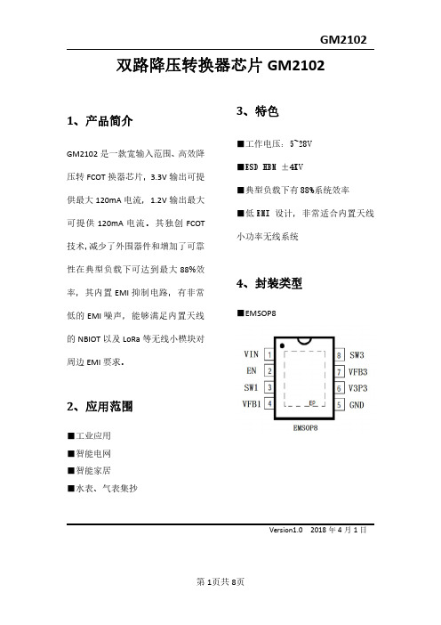
GM2102双路降压转换器芯片GM21021、产品简介GM2102是一款宽输入范围、高效降压转FCOT换器芯片,3.3V输出可提供最大120mA电流,1.2V输出最大可提供120mA电流。
其独创FCOT 技术,减少了外围器件和增加了可靠性在典型负载下可达到最大88%效率,其内置EMI抑制电路,有非常低的EMI噪声,能够满足内置天线的NBIOT以及LoRa等无线小模块对周边EMI要求。
2、应用范围■工业应用■智能电网■智能家居■水表、气表集抄3、特色■工作电压:5~28V■ESD HBM±4KV■典型负载下有88%系统效率■低EMI设计,非常适合内置天线小功率无线系统4、封装类型■EMSOP85、功能引脚定义序号名称说明1VIN电源输入2EN使能3SW1 1.2V开关管端口4VFB1 1.2V反馈5GND地6V3P3 1.2V DCDC输入电压端口7VFB3 3.3V反馈8SW3 3.3V开关管端口6、典型应用电路图1典型应用电路图7、极限参数符号说明大小单位VIN最大电源电压30V SW3 3.3V开关管端口电压GND-0.3~28V SW1 1.2V开关管端口电压GND-0.3~5.5V VFB1 1.1V反馈电压GND-0.3~5.5V VFB3 3.3V反馈电压GND-0.3~5.5VV3P3 3.3V电压GND-0.3~5.5VEN使能电压GND-0.3~5.5VTj最大结温170℃Θja热阻40℃/W Tstg储存温度-60~160℃Pd1最大消耗功率(SOT23-5)0.5WESD HBM4000V 8、电气特性直流特性(VIN=12V,L=3.3uH,TA=+25℃,除非特别注明)参数符号条件最小典型最大单位供电电压VIN71228V空载工作电流IQ400800μAFB反馈电压VFB3 1.1 1.17 1.25V VFB10.650.700.75VFB输入电流VFB3000nA VFB1000nA开关频率FSW 3.3uH电感,负载电流120mA600KHZUVLO VIN=12VVin=3.3V12to3.3dcdc3.3to1.1dcdc52.8VUVLO_HYS0.1V 使能电压EN 2.55V 使能迟滞EN_HYS3V 使能上拉电阻85K R 关断静态电流IQD500u开关导通时间TON VIN=12V,VOUT=3.3VVIN=3.3V,VOUT=1.1V350500nS开关电阻Ron SW3SW1500300mRmR9、典型特性VOUT3P3IL=10~120mAVOUT1P1IL=10~120mAEMI测试,知用EM5030-3探头(20dB衰减),EMI检波方式10、封装外形尺寸EMSOP8广州国梦电子科技有限公司电话:一八六二〇一四〇一五六刘经理E-mail:lyf_gmdz@。

IPV3 LI 介绍加中文使用说明书产品规格输出功率:10W – 165W / 5J – 50J输出电压:1.0V – 7.5V输入电流:1.3A – 40.0A输入电压:6.2V – 8.5V标准(功率模式:Power Mode)雾化器电阻:0.1ohm – 3.0ohm 焦耳模式(Joules Mode) 雾化器电阻:0.05ohm – 0.3ohm温度限制摄氏度:100℃ - 300℃温度限制华氏度:212℉ - 572℉效能:95%屏幕尺寸:0.96”OLED芯片:YIHI SX330-v3SL主要功能可视化操作系统低电压保护低电阻保护高输入电压预警输出短路保护电池反向保护温度过热保护软件更新/图形操作界面温度控制(100℃ - 300℃ / 212℉ - 572℉)支持200W更新使用说明1、开/关机快速连续按下点火键5次开启设备。
如果开机成功,你可以在屏幕上看到“Pioneer4you”、”iPV3-Li”,然后进入待机模式。
在待机模式下,快速连续按下点火键5次进入菜单模式,当你看到”System On”时,按下“+”键关闭设备。
2、温度限制功能在待机模式下,快速连续按下点火键5次进入菜单模式。
菜单模式下可以通过按下点火键切换不同功能的设置。
设置内容包含:SYSTEM、MODE、UNIT、TEMP、EXIT。
切到到对应设置界面下,按下”+”或”-”键可以进行调整。
SYSTEM:开/关机,默认为ON,按下“+”键则关闭设备。
MODE:模式选择,POWER为功率模式,JOULE为焦耳模式即温控。
UNIT:温度单位选择,C为摄氏度,F为华氏度(科普:转换公式为:f=c*9/5 32)。
TEMP:温度设置,可以按下”+”和”-”键增减设置。
EXIT:退出菜单,默认为ON,按下“+”键则退出菜单模式。
(1)在模式(MODO)菜单下,按下”+”或”-”键可以切换功率模式(POWER)和焦耳模式(JOULE)。
40V高输入电压LDO线性稳压器一般说明PW6206系列是一款高精度,高输入电压,低静态电流,高速,低压降线性稳压器具有高纹波抑制。
在VOUT=5V&VIN=7V时,输入电压高达40V,负载电流高达300mA,采用BCD工艺制造。
PW6206提供过电流限制、软启动和过热保护,以确保设备在良好的条件下工作PW6206调节器有标准SOT89-3L和SOT23-3L封装。
标准产品无铅无卤。
特点⚫输入电压:4.75V~40V⚫输出电压:1.8V~5.7V⚫输出精度:<±2%⚫输出电流:150mA(典型值)⚫最高300mA@VIN=7V,VOUT=5V,PW6206B50HV封装⚫电源抑制比:60dB@100Hz⚫跌落电压:600mV@IOUT=100mA⚫静态电流:4.2μA@VIN=12V(典型值)⚫ESD HBM:8KV⚫推荐电容器:10uF应用芯片135代2845理8039⚫智能电表⚫车内娱乐⚫电动自行车典型应用电路应用信息 输入电容器VIN 和GND 引脚之间需要10μF 的输入电容。
电容器应尽可能靠近VIN 引脚,建议使用电解电容器。
必须考虑公差和温度系数,以确保电容器在整个温度和工作条件范围内工作。
输出电容器在实际应用中,选择输出电容器以保证其稳定运行是非常重要的。
稳定和正确操作的最小电容为1μF。
电容公差应在工作温度范围内±30%或更好。
建议电容器类型为MLCC。
空载稳定性PW6206将在无外部负载的情况下保持稳定和调节。
这在CMOS RAM保持活动应用中尤其重要。
典型电路下图显示了PW6206设备的典型应用电路。
根据应用情况,应仔细选择外部组件的值。
在插拔应用中,由于芯片上电源的插入和拔出引起的过冲会损坏芯片,因此建议VIN小于30V,输入电压峰值不超过45V。
在高输入应用中,建议R、Cin选用如下:1Cin=10UF~100UF电解电容器,最大电压大于50V,R=0;2Cin=1UF~10UF MLCC,最大电压V大于50V,R=2Ω,1206型电阻器应仔细选择,以确保有足够的裕度来承受插入期间的浪涌电流。
广州唯创电子有限公司MP3录音模块WTN1XXX系列语音芯片说明书Note:WAYTRONIC ELECTRONIC CO.,LTD.reserves the right to change this document without prior rmation provided by WAYTRONIC is believed to be accurate and reliable.However,WAYTRONIC makes no warranty for any errors which may appear in this document.Contact WAYTRONIC to obtain the latest version of device specifications before placing your orders.No responsibility is assumed by WAYTRONIC for any infringement of patent or other rights of third parties which may result from its use.In目录1.概述: (2)2.功能简述: (2)3.管脚描述: (2)4.极限参数: (3)5.播放速率: (3)6.单线脉冲触发: (3)7.按键控制方式: (5)8.程序范例 (6)9.应用电路 (8)10.封装管脚图 (9)我司说明书以业务员和公司官网的为准1.概述:WTN1系列为全新世代高性价比的语音芯片,具有9bits高性能PWM/DAC语音引擎。
并且具备有5~20秒(6K/4bits)多样化的型号选择,并内置有高精准度起振器,毋需外部起振组件,外接组件少,让应用开发整体成本具有市场领先的优势。
2.功能简述:(1)工作电压:2.0V~5.0V(2)具备串口控制模式:数脉冲,按键控制(3)语音引擎:9bits PWM./9bits DAC(部分型号无DAC功能)(4)可编辑阶数:3800(5)阶可编辑群组数:63组(最大)(6)开机执行群组:1(7)组可放声音长度:/10(WTN1010)/20(WTN1020)(8)内置RC震荡起振回路选型注意:1.芯片的控制方式和输出方式在烧写程序时已经设定好,不可以再次更改,订做芯片时需要和业务员说明应用要求。
1A Low Dropout Positive Voltage RegulatorLM1117L3Features Description●Adjustable or Fixed Output The LM1117 series of positive adjustable and fixed ●Output Current of 1A regulators are designed to provide 1A with high ●Low Dropout, 1.3V max at 1A Output Current efficiency. All internal circuitry is designed to ●0.04% Line Regulation operate down to 1.3V input to output differential. ●0.2% Load Regulation On-chip trimming adjusts the reference voltage to ●100% Thermal Limit Burn-in 1%.●Fast Transient ResponseApplications●High Efficiency Linear Regulators● Post Regulators for Switching Supplies● Adjustable Power SupplyTypical Application DataFixed V oltage RegulatorAdjustable V oltage RegulatorV OUT =V REF ×(1+R2/R1)+I ADJ ×R21) C1 needed if device is far from filter capacitors2) C2 minimum value required for stabilityC2 10μF Tant.MinV OUT =3.3V C110μF Tant V IN >4.75V 1 23IN TAB GND OUT +V OUT =3.45V C2 10μF Tant.Min R2 232 Ohm,1%C1 10μF, Tant V IN >4.75V + IN TAB ADJ OUT+Package InformationSOT-223Absolute Maximum RatingsSymbol ParameterMaximum Units PD Power DissipationInternally Limited W VIN Input Voltage7 V TJ Operating Junction Temperature RangeControl SectionPower Transistor0 to 125 0 to 150 ℃ TSTG Storage Temperature-65 to 150 ℃ TLEAD Lead Temperature(Soldering, 10 sec) 300 ℃Device Selection GuideDeviceOutput Voltage LM1117-AdjAdjustable LM1117-1.51.5V LM1117-1.81.8V LM1117-2.52.5V LM1117-2.852.8 5V LM1117-3.03. 0V LM1117-3.33.3V LM1117-3.53.5V LM1117-5.05.0VElectrical Characteristics @I LOAD =0mA,T J =25℃, unless otherwise specifiedParameter DeviceTest Conditions Min Typ Max Units V IN =5V,I LOAD =10mA 1.238 1.250 1.262Reference voltage(Note 1) Adj VersionV IN =2.65V to 7V,I LOAD =10mA to 1A * 1.225 1.250 1.275V V IN =V OUT +1.5VVariator from nominal V OUT-1 +1 % V IN =V OUT +1.5V to 7VI LOAD =0mA to 1AOutput Voltage (Note 1) Al fixedversion Variator from nominal V OUT * -2 +2 %Line Regulation (Note 1) All I LOAD =10mA,(V OUT +1.5V)≦V ≦7V * 0.040.2Load Regualtion (Note 1) All V IN =V OUT +1.5V, I LOAD =10mA to 1A * 0.2 0.4%Minimum Load Current Adj Version V IN =5V,V ADJ =0V * 3 7mAGround Pin Current All fixed version V IN =V OUT +1.5V,I LOAD =10mA to 1A *713mAAdjust Pin CurrentAdj Version V IN =2.65V to 7V, I LOAD =10mA * 55 90µA Pin Function1 ADJ/GND2 OUTPUT3 INPUT 1 2 3Current Limit All (V IN -V OUT )=1.5V* 1 A Ripple Rejection (Note 2)All V IN =V OUT +1.5V,I LOAD =1A6072dB Dropout Voltage (Note 1,3)All V IN ≧2.65V, I LOAD = 1A* 1.15 1.3V Temperature CoefficientAll V IN =V OUT=1.5V, I LOAD = 10mA * 0.005 %/℃The * denotes the specifications which apply over the full temperature range.Note 1:Low duty pulse testing with Kelvin connections required.Note 2:120Hz input ripple(CADJ for ADJ=25μF)Note 3:△VOUT, △VREF=1%.Representative Circuit DiagramGND V INV OUT FOR FIXEDVOLTAGEDEVICEFORADJUSTABLEVOLTAGEDEVICE ADJ*: TypicalInches Millimeters Inches Millimeters DIM Min. Max. Min. Max. DIM Min. Max. Min. Max.A 0.1142 0.1220 2.90 3.10 G 0.0551 0.0709 1.40 1.80B 0.2638 0.2874 6.70 7.30 H 0.0098 0.0138 0.25 0.35C 0.1299 0.1457 3.30 3.70 I 0.0008 0.0039 0.02 0.10D 0.0236 0.0315 0.60 0.80 a1 *13o - *13o -E *0.0906 - *2.30 - a2 0 o 10 o 0 o 10 oF 0.2480 0.2638 6.30 6.70Notes: 1.Controlling dimension: millimeters.2.Maximum lead thickness includes lead finish thickness, and minimum lead thickness is the minimum thickness of base material.3.If there is any question with packing specification or packing method, please contact your local CYStek sales office. Material:• Lead: 42 Alloy; solder plating• Mold Compound: Epoxy resin family, flammability solid burning class: UL94V-0Important Notice:• All rights are reserved. Reproduction in whole or in part is prohibited without the prior written approval of CYStek.• CYStek reserves the right to make changes to its products without notice.• CYStek semiconductor products are not warranted to be suitable for use in Life-Support Applications, or systems.• CYStek assumes no liability for any consequence of customer product design, infringement of patents, or application assistance.321FB AC D EG H a1a2I Style: Pin 1.Adj/Gnd 2.Output3.Input3-Lead SOT-223 Plastic Surface Mounted PackageCYStek Package Code: L3左一: 西元年末碼左二: 月碼, 1=A,2=B,…8=H,9=J, …,12=M左三-四: 流水號 Date CodePart number:XX: 15 for 1.5V18 for 1.8V25 for 2.5V33 for 3.3V50 for 5.0VBlank for ADJ。
PW5410BGENERAL DESCRIPTIONThe PW5410B is a low noise, constant frequency (1.2MHz) switched capacitor voltage doubler. It produces a regulated output voltage from 1.8V to 5V input with up to 100mA of output current. Low external parts count (one flying capacitor and two small bypass capacitors at VIN and VOUT) make the PW5410B ideally suited for small, battery-powered applications.The new charge-pump architecture maintains constant switching frequency to no load and reduces both output and input ripple. The PW5410B have thermal shutdown capability and can survive a continuous short circuit from VOUT to GND. Built-in soft-start circuitry prevents excessive inrush current during start-up.FEATURES● Fixed 3.3V±4% Output ● VIN Range: 1.8V ~ 5V● Output Current: up to 250mA (VIN=3V) ● Low Noise Constant Frequency Operation ● Shutdown Current: <1μA ● Short-Circuit Protection ● Soft-start ● No Inductors●Available in Low Profile 6-Lead SOT-23 PackageAPPLICATIONS● White LED Backlighting● Li-Ion Battery Backup Supplies ● Local 3V to 5V Conversion ● Smart Card Readers●PCMCIA Local 5V SuppliesTYPICAL APPLICATION CIRCUITPW5410BRegulated 3.3V OutputParameter VALUE UnitInput Supply Voltage -0.3V ~ 6VEN Pin Voltage -0.3V ~ 6VOutput Voltage -0.3V ~ 3.5VOutput Current 300 mAOperating Temperature Range (Note 2)) -40℃ ~ +85 °CMaximum Junction Temperature +150 °CStorage Temperature Range -65℃ ~ +125°CLead Temperature (Soldering, 10 sec.) +265 °CNote 1: Stresses listed as the above “Absolute Maximum Ratings” may cause permanent damage to the device. Exposure to absolute maximum rating conditions for extended periods may remain possibility to affect device reliability.Note 2: The PW5410B is guaranteed to meet performance specifications from 0℃ to 70℃. Specifications over the –40℃ to 85℃ operating temperature range are assured by design, characterization and correlation with statistical process controls.ELECTRICAL CHARACTERISTICS(Operating Conditions: TA = 25℃, VIN = 3.6V, VEN = VIN, CIN = COUT = 2.2μF, unless otherwise noted.) SYMBOL PARAMETER CONDITIONS MIN TYP MAX UNITS VIN Input Voltage Range 1.8 5 VVOUT Output VoltageRange3.17 3.3 3.43 VISHDN Shutdown Current VEN = 0V, VOUT = 0V0.2 μAINO LOAD No load inputcurrentIOUT = 0mA, VIN = 2.7V0.65 mAfOSC Switching Frequency VIN = 2.7V, IOUT = 100mA 1.2 MHz Block DiagramNo Load Supply Current vs. SupplyOutput Voltage vs. Supply VoltageOscillator Frequency vs.Supply Voltage Short Circuit Current vs. Supply Voltage(IOUT=0A)3.23.213.223.233.243.253.263.273.283.293.32.533.544.55Supply Voltage (V)O u t p u t V o l t a g e (V )Voltage00.10.20.30.40.50.60.70.80.912.533.544.55Supply Voltage (V)S u p p l y C u r r e n t (m A )0.50.60.70.80.911.11.21.31.41.52.53 3.54 4.55 Supply Voltage (V)O s c i l l a t o r F r e q u e n c y (M H z )03060901201501802102402703002.53 3.54 4.55Supply Voltage (V)S h o r t C i r c u i t C u r r e n t (m A )OperationThe PW5410B use a switched capacitor charge pump to boost VIN to a regulated output voltage. Regulation is achieved by sensing the output voltage through an internal resistor divider and modulating the charge pump output current based on the error signal. A 2-phase nonoverlapping clock activates the charge pump switches. The flying capacitor is charged from VIN on the first phase of the clock. On the second phase of the clock it is stacked in series with VIN and connected to VOUT. This sequence of charging and discharging the flying capacitor continues at a free running frequency of 1.2MHz (typ).In shutdown mode all circuitry is turned off and the PW5410B draw only leakage current from the VIN supply. Furthermore, VOUT is disconnected from VIN. The EN pin is a CMOS input with a threshold voltage of approximately 0.8V. The PW5410B is in shutdown when a logic low is applied to the EN pin. Since the EN pin is high impedance CMOS input it should never be allowed to float. To ensure that its state is defined it must always be driven with a valid logic level.Short-Circuit ProtectionThe PW5410B have built-in short-circuit current limiting. At short-circuit condition, it will automatically limit the output current to approximately 300mA.Soft-StartThe PW5410B have built-in soft-start circuitry to prevent excessive current flow at VIN during start-up. The soft-start time is preprogrammed to approximately 2.5ms, so the start-up current will be primarily dependent upon the output capacitor.VIN, VOUT Capacitor SelectionThe style and value of capacitors used with the PW5410B determine several important parameters such as regulator control loop stability, output ripple, charge pump strength and minimum start-up time. To reduce noise and ripple, it is recommended that low ESR (<0.1Ω) ceramic capacitors be used for both CIN and COUT. These capacitors should be 2.2μF or greater. Tantalum and aluminum capacitors are not recommended because of their high ESR.Flying Capacitor SelectionWarning: A polarized capacitor such as tantalum or aluminum should never be used for the flying capacitor since its voltage can reverse upon start-up of the PW5410B. Low ESR ceramic capacitors should always be used for the flying capacitor. The flying capacitor controls the strength of the charge pump. In order to achieve the rated output current it is necessary to have at least 2.2μF of capacitance for the flying capacitor.SOT23-6LSymbolDimensions In Millimeters Dimensions In Inches MinMaxMinMaxA 1.050 1.250 0.041 0.049 A1 0.000 0.100 0.000 0.004 A2 1.0501.1500.041 0.045b 0.300 0.500 0.012 0.020c 0.100 0.200 0.004 0.008 D 2.820 3.020 0.111 0.119 E 1.500 1.700 0.059 0.067 E1 2.6502.9500.104 0.116e 0.950(BSC) 0.037(BSC)e1 1.800 2.000 0.071 0.079 L 0.300 0.600 0.012 0.024θ 0°8°0°8°。