A CMOS Voltage Controlled Ring Oscillator with Improved Frequency Stability
- 格式:pdf
- 大小:157.21 KB
- 文档页数:9
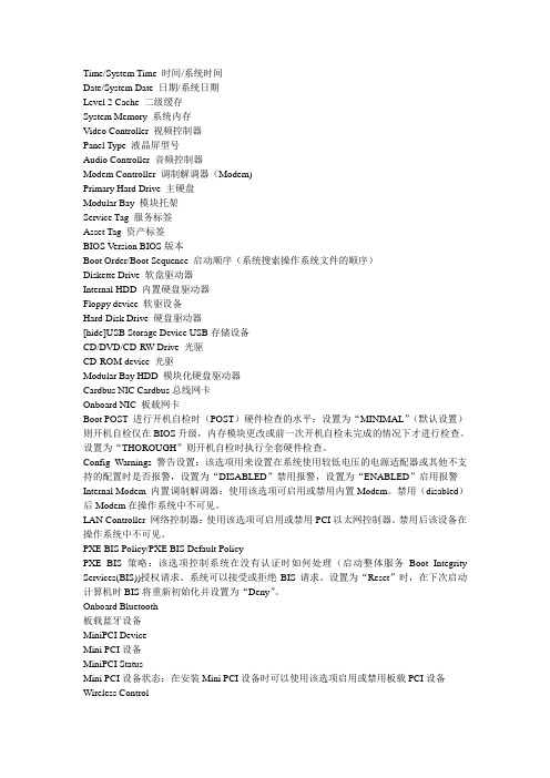
Time/System Time 时间/系统时间Date/System Date 日期/系统日期Level 2 Cache 二级缓存System Memory 系统内存Video Controller 视频控制器Panel Type 液晶屏型号Audio Controller 音频控制器Modem Controller 调制解调器(Modem)Primary Hard Drive 主硬盘Modular Bay 模块托架Service Tag 服务标签Asset Tag 资产标签BIOS Version BIOS版本Boot Order/Boot Sequence 启动顺序(系统搜索操作系统文件的顺序)Diskette Drive 软盘驱动器Internal HDD 内置硬盘驱动器Floppy device 软驱设备Hard-Disk Drive 硬盘驱动器[hide]USB Storage Device USB存储设备CD/DVD/CD-RW Drive 光驱CD-ROM device 光驱Modular Bay HDD 模块化硬盘驱动器Cardbus NIC Cardbus总线网卡Onboard NIC 板载网卡Boot POST 进行开机自检时(POST)硬件检查的水平:设置为“MINIMAL”(默认设置)则开机自检仅在BIOS升级,内存模块更改或前一次开机自检未完成的情况下才进行检查。
设置为“THOROUGH”则开机自检时执行全套硬件检查。
Config Warnings 警告设置:该选项用来设置在系统使用较低电压的电源适配器或其他不支持的配置时是否报警,设置为“DISABLED”禁用报警,设置为“ENABLED”启用报警Internal Modem 内置调制解调器:使用该选项可启用或禁用内置Modem。
禁用(disabled)后Modem在操作系统中不可见。
LAN Controller 网络控制器:使用该选项可启用或禁用PCI以太网控制器。
1)当打开变成搜索一日,笔者在更换文件夹那难看的图标后,大功告成的想看看效果,但双击文件夹却半天没反应,最后却跳出来个搜索对话框,这可如何是好。
又试了试其他文件夹才知道全都变成这样,想到刚才修改了图标,觉得肯定是改的出了问题。
于是又将原来的默认的图标改回来,但还是如此。
我有将驱动器的图标给该了,这下连驱动器的打开也变成了搜索。
只能通过右击打开。
看来是又玩过头了,怎么拌,只好发扬一下DIY 精神L。
既然与打开方式有关,最后想到注册表。
[hkey_CLASSES_ROOT\Directory\shell]开始没看出什么异常,和其他机子一比较才发现原来的Shell键值是none,而现在却变成了find,于是将其改回,按下键盘F5刷新一切恢复正常。
又将一番试验,其实将其Shell键删除也可以解决问题。
2)文件夹双击打不开解决办法在我们使用电脑有过程中,大部分时间我们的爱机还是够听话的,但偶尔也会罢工 ,今天就说一下文件夹双击打不开的问题。
有时只是闪一下就完事了,有时却打开了搜索等其它东西。
但大部分问题右击选择打开还是能打开的,下面是我通常用的几种解决办法。
1.鼠标太灵敏。
这种可能性还是比较小的。
但这种方法却是最简单的。
解决方法:运行—control 打开控制面板,找见打印机和其它硬件中的鼠标选项。
在“鼠标键”选项卡中将“双击速度”调整到合适的位置,同时在右边的图标上可以测试文件夹打开速度。
其实这个快慢是说双击间隔的时间的,如果设置的太快(间隔时间短),我们双击间隔的时间大于设定的时间就打不开了。
2.病毒破坏致关联文件打开方式丢失这种情况可能性是最大的,因为一般的文件夹双击打不开都是病毒在捣乱。
而且右击文件夹第一个选项就是搜索等选项。
解决方法:首先更新杀毒软件最新病毒特征库,全盘杀毒。
病毒杀不了就会后患无穷,即使将关联方式改回来也会再被病毒破坏。
在文件夹选项中将隐藏文件显示出来。
如图:有的时候,病毒会为了防止它的配置文件被我们删除就会改动注册表达到彻底隐藏文件的目的,这时即使我们根据上面的设置将隐藏文件显示也不奏效。
MC145151–2 through MC145158–21MOTOROLAMC145151–2 through MC145158–25MC145151–2 through MC145158–29MC145151–2 through MC145158–213MC145151–2 through MC145158–2MOTOROLA15OUTPUT PINSPD outPhase Detector A Output (Pin 6)Three–state output of phase detector for use as loop–error signal. Double–ended outputs are also available for this pur-pose (see φV and φR ).Frequency f V > f R or f V Leading: Negative Pulses Frequency f V < f R or f V Lagging: Positive PulsesFrequency f V = f R and Phase Coincidence: High–Imped-ance State φR , φVPhase Detector B Outputs (Pins 4, 3)These phase detector outputs can be combined externally for a loop–error signal. A single–ended output is also avail-able for this purpose (see PD out ).If frequency f V is greater than f R or if the phase of f V is leading, then error information is provided by φV pulsing low.φR remains essentially high.If the frequency f V is less than f R or if the phase of f V is lagging, then error information is provided by φR pulsing low.φV remains essentially high.If the frequency of f V = f R and both are in phase, then both φV and φR remain high except for a small minimum time period when both pulse low in phase.MCDual–Modulus Prescale Control Output (Pin 8)Signal generated by the on–chip control logic circuitry for controlling an external dual–modulus prescaler. The MC level will be low at the beginning of a count cycle and will remain low until the ÷ A counter has counted down from its pro-grammed value. At this time, MC goes high and remains high until the ÷ N counter has counted the rest of the way down from its programmed value (N – A additional counts since both ÷ N and ÷ A are counting down during the first portion of the cycle). MC is then set back low, the counters preset totheir respective programmed values, and the above se-quence repeated. This provides for a total programmable divide value (N T ) = N P + A where P and P + 1 represent the dual–modulus prescaler divide values respectively for high and low MC levels, N the number programmed into the ÷ N counter, and A the number programmed into the ÷ A counter.LDLock Detector Output (Pin 9)Essentially a high level when loop is locked (f R , f V of same phase and frequency). LD pulses low when loop is out of lock.SW1, SW2Band Switch Outputs (Pins 14, 15)SW1 and SW2 provide latched open–drain outputs corre-sponding to data bits numbers one and two. These outputs can be tied through external resistors to voltages as high as 15 V, independent of the V DD supply voltage. These are typically used for band switch functions. A logic 1 causes the output to assume a high–impedance state, while a logic 0causes the output to be low.REF outBuffered Reference Oscillator Output (Pin 17)Buffered output of on–chip reference oscillator or externally provided reference–input signal.POWER SUPPLYV DDPositive Power Supply (Pin 5)The positive power supply potential. This pin may range from + 3 to + 9 V with respect to V SS .V SSNegative Power Supply (Pin 7)The most negative supply potential. This pin is usually ground.MC145151–2 through MC145158–217MOTOROLAOUTPUT PINSPD outPhase Detector A Output (Pin 5)This single–ended (three–state) phase detector output pro-duces a loop–error signal that is used with a loop filter to con-trol a VCO.Frequency f V > f R or f V Leading: Negative Pulses Frequency f V < f R or f V Lagging: Positive Pulses Frequency f V = f R and Phase Coincidence: High–Imped-ance StateφR, φVPhase Detector B Outputs (Pins 16, 15)Double–ended phase detector outputs. These outputs can be combined externally for a loop–error signal. A single–ended output is also available for this purpose (see PD out). If frequency f V is greater than f R or if the phase of f V is leading, then error information is provided by φV pulsing low.φR remains essentially high.If the frequency f V is less than f R or if the phase of f V is lagging, then error information is provided by φR pulsing low.φV remains essentially high.If the frequency of f V = f R and both are in phase, then both φV and φR remain high except for a small minimum time period when both pulse low in phase.MCDual–Modulus Prescale Control Output (Pin 12)This output generates a signal by the on–chip control logic circuitry for controlling an external dual–modulus prescaler. The MC level is low at the beginning of a count cycle and remains low until the ÷ A counter has counted down from its programmed value. At this time, MC goes high and remains high until the ÷ N counter has counted the rest of the way down from its programmed value (N – A additional counts since both ÷ N and ÷ A are counting down during the first por-tion of the cycle). MC is then set back low, the counters preset to their respective programmed values, and the above se-quence repeated. This provides for a total programmable di-vide value (N T) = N P + A where P and P + 1 represent the dual–modulus prescaler divide values respectively for high and low modulus control levels, N the number programmed into the ÷ N counter, and A the number programmed into the ÷ A counter. Note that when a prescaler is needed, the dual–modulus version offers a distinct advantage. The dual–modu-lus prescaler allows a higher reference frequency at the phase detector input, increasing system performance capa-bility, and simplifying the loop filter design.f R, f VR Counter Output, N Counter Output (Pins 13, 3) Buffered, divided reference and f in frequency outputs. The f R and f V outputs are connected internally to the ÷ R and ÷ N counter outputs respectively, allowing the counters to be used independently, as well as monitoring the phase detector inputs.LDLock Detector Output (Pin 7)This output is essentially at a high level when the loop is locked (f R, f V of same phase and frequency), and pulses low when loop is out of lock.REF outBuffered Reference Oscillator Output (Pin 14)This output can be used as a second local oscillator, refer-ence oscillator to another frequency synthesizer, or as the system clock to a microprocessor controller.POWER SUPPLYV DDPositive Power Supply (Pin 4)The positive power supply potential. This pin may range from + 3 to + 9 V with respect to V SS.V SSNegative Power Supply (Pin 6)The most negative supply potential. This pin is usually ground.。
TOP252-262TOPSwitch-HX Family January 2009Enhanced EcoSmart ®, Integrated Off-Line Switcher with Advanced Feature Set and Extended Power Range®Product HighlightsLower System Cost, Higher Design FlexibilityMulti-mode operation maximizes efficiency at all loads New eSIP-7F and eSIP-7C packagesLow thermal impedance junction-to-case (2 °C per watt)Low height is ideal for adapters where space is limitedSimple mounting using a clip to aid low cost manufacturing Horizontal eSIP-7F package ideal for ultra low height adapter and monitor applicationsExtended package creepage distance from DRAIN pin to adjacent pin and to heat sinkNo heatsink required up to 35 W using P , G and M packages with universal input voltage and up to 48 W at 230 VACOutput overvoltage protection (OVP) is user programmable for latching/non-latching shutdown with fast AC reset Allows both primary and secondary sensingLine undervoltage (UV) detection prevents turn-off glitches Line overvoltage (OV) shutdown extends line surge limit Accurate programmable current limitOptimized line feed-forward for line ripple rejection132 kHz frequency (254Y-258Y and all E/L packages) reduces transformer and power supply sizeHalf frequency option for video applications Frequency jittering reduces EMI fi lter cost •••••••••••••••••Figure 1. Typical Flyback Application.Heatsink is connected to SOURCE for low EMIImproved auto-restart delivers <3% of maximum power in short circuit and open loop fault conditionsAccurate hysteretic thermal shutdown function automatically recovers without requiring a resetFully integrated soft-start for minimum start-up stress Extended creepage between DRAIN and all other pins improves fi eld reliability•••••Table 1.Output Power Table. (for notes see page 2).Rev. F 01/09EcoSmart ®– Energy Effi cientEnergy efficient over entire load range No-load consumptionLess than 200 mW at 230 VAC Standby power for 1 W input>600 mW output at 110 VAC input >500 mW output at 265 VAC inputDescriptionTOPSwitch-HX cost effectively incorporates a 700 V power MOSFET, high voltage switched current source, PWM control, oscillator, thermal shutdown circuit, fault protection and other control circuitry onto a monolithic device.••••••Figure 2. Typical Flyback Application TOP259YN, TOP260YN and TOP261YN.Y Package Option for TOP259-261In order to improve noise-immunity on large TOPSwitch-HX Y package parts, the F pin has been removed (TOP259-261YN are fi xed at 66 kHz switching frequency) and replaced with a SIGNAL GROUND (G) pin. This pin acts as a low noise path for the C pin capacitor and the X pin resistor. It is only required for the TOP259-261YN package parts.Notes for Table 1:1. Minimum continuous power in a typical non-ventilatedenclosed adapter measured at +50 °C ambient. Use of an external heat sink will increase power capability. 2. Minimum continuous power in an open frame design at+50 °C ambient.3. Peak power capability in any design at +50 °C ambient.4. 230 VAC or 110/115 VAC with doubler.5. Packages: P: DIP-8C, G: SMD-8C, M: SDIP-10C,Y: TO-220-7C, E: eSIP-7C, L: eSIP-7F .See part ordering information.6. TOP261 and TOP262 have the same current limit set point. Insome applications TOP262 may run cooler than TOP261 due to a lower R DS(ON) for the larger device.7. TOP256E package parts are available with Green (HalogenFree) mold compound. See Part Ordering Information on page 47. Parametrically green material encapsulated E package parts are identical to non-green parts. Section ListFunctional Block Diagram (4)Pin Functional Description (6)TOPSwitch-HX Family Functional Description (7)CONTROL (C) Pin Operation (8)Oscillator and Switching Frequency (8)Pulse Width Modulator (9)Maximum Load Cycle (9)ErrorAmplifier (9)On-Chip Current Limit with External Programmability (9)Line Under-Voltage Detection (UV) (10)Line Overvoltage Shutdown (OV) (11)Hysteretic or Latching Output Overvoltage Protection (OVP) (11)Line Feed-Forward with DCMAX Reduction (13)Remote ON/OFF and Synchronization (13)Soft-Start (13)Shutdown/Auto-Restart (13)Hysteretic Over-Temperature Protection (13)BandgapReference (13)High-Voltage Bias Current Source (13)Typical Uses of FREQUENCY (F) Pin (15)Typical Uses of VOLTAGE MONITOR (V) and EXTERNAL CURRENT LIMIT (X) Pins (16)Typical Uses of MULTI-FUNCTION (M) Pin (18)Application Examples (21)A High Effi ciency, 35 W, Dual Output – Universal Input Power Supply (21)A High Effi ciency, 1500 W, 250-380 VDC Input Power Supply (22)A High Effi ciency, 20 W Continuous – 80 W Peak, Universal Input Power Supply (23)A High Effi ciency, 65 W, Universal Input Power Supply (24)Key Application Considerations (25)TOPSwitch-HX vs.TOPSwitch-GX (25)TOPSwitch-HX Design Considerations (26)TOPSwitch-HX Layout Considerations (27)Quick Design Checklist (31)DesignTools (31)Product Specifi cations and Test Conditions (32)Typical Performance Characteristics (39)Package Outlines (43)Part Ordering Information (47)Rev. F 01/09Rev. F 01/09Figure 3a. Functional Block Diagram (P and G Packages).Figure 3b. Functional Block Diagram (M Package).Rev. F 01/09Figure 3c. Functional Block Diagram (TOP254-258 YN Package and all eSIP Packages).Figure 3d. Functional Block Diagram TOP259YN, TOP260YN, TOP261YN.Rev. F 01/09Pin Functional DescriptionDRAIN (D) Pin:High-voltage power MOSFET DRAIN pin. The internal start-up bias current is drawn from this pin through a switched high-voltage current source. Internal current limit sense point for drain current.CONTROL (C) Pin:Error amplifi er and feedback current input pin for duty cycle control. Internal shunt regulator connection to provide internal bias current during normal operation. It is also used as the connection point for the supply bypass and auto-restart/compensation capacitor.EXTERNAL CURRENT LIMIT (X) Pin (Y, M, E and L package):Input pin for external current limit adjustment and remote ON/OFF. A connection to SOURCE pin disables all functions on this pin.Figure 4. Pin Confi guration (Top View).P I -4711-021308Figure 5. TOP254-258 Y and All M/E/L Package Line Sense and Externally Set Current Limit.Figure 7. P/G Package Line Sense.P I -4983-021308Figure 6. TOP259-261 Y Package Line Sense and External Current Limit.VOLTAGE MONITOR (V) Pin (Y & M package only):Input for OV, UV, line feed forward with DC MAX reduction, output overvoltage protection (OVP), remote ON/OFF and device reset. A connection to the SOURCE pin disables all functions on this pin.MULTI-FUNCTION (M) Pin (P & G packages only):This pin combines the functions of the VOLTAGE MONITOR (V) and EXTERNAL CURRENT LIMIT (X) pins of the Y package into one pin. Input pin for OV, UV, line feed forward with DC MAXRev. F 01/09Figure 8. P/G Package Externally Set Current Limit.reduction, output overvoltage protection (OVP), external current limit adjustment, remote ON/OFF and device reset. Aconnection to SOURCE pin disables all functions on this pin and makes TOPSwitch-HX operate in simple three terminal mode (like TOPSwitch-II).FREQUENCY (F) Pin (TOP254-258Y, and all E and L packages):Input pin for selecting switching frequency 132 kHz if connected to SOURCE pin and 66 kHz if connected to CONTROL pin. The switching frequency is internally set for fi xed 66 kHzoperation in the P , G, M package and TOP259YN, TOP260YN and TOP261YN.SIGNAL GROUND (G) Pin (TOP259YN, TOP260YN & TOP261YN only):Return for C pin capacitor and X pin resistor.SOURCE (S) Pin:Output MOSFET source connection for high voltage power return. Primary side control circuit common and reference point.TOPSwitch-HX Family Functional DescriptionLike TOPSwitch-GX, TOPSwitch-HX is an integrated switched mode power supply chip that converts a current at the control input to a duty cycle at the open drain output of a high voltage power MOSFET. During normal operation the duty cycle of the power MOSFET decreases linearly with increasing CONTROL pin current as shown in Figure 9.In addition to the three terminal TOPSwitch features, such as the high voltage start-up, the cycle-by-cycle current limiting, loop compensation circuitry, auto-restart and thermalshutdown, the TOPSwitch-HX incorporates many additional functions that reduce system cost, increase power supply performance and design fl exibility. A patented high voltageCMOS technology allows both the high-voltage power MOSFET and all the low voltage control circuitry to be cost effectively integrated onto a single monolithic chip.Three terminals, FREQUENCY, VOLTAGE-MONITOR, andEXTERNAL CURRENT LIMIT (available in Y and E/L packages),two terminals, VOLTAGE-MONITOR and EXTERNAL CURRENT LIMIT (available in M package) or one terminal MULTI-FUNCTION (available in P and G package) have been used to implement some of the new functions. These terminals can be connected to the SOURCE pin to operate the TOPSwitch-HX in aTOPSwitch-like three terminal mode. However, even in this three terminal mode, the TOPSwitch-HX offers many transparent features that do not require any external components:A fully integrated 17 ms soft-start significantly reduces or eliminates output overshoot in most applications by sweeping both current limit and frequency from low to high to limit the peak currents and voltages during start-up.A maximum duty cycle (DC MAX ) of 78% allows smaller inputstorage capacitor, lower input voltage requirement and/or higher power capability.Multi-mode operation optimizes and improves the powersupply effi ciency over the entire load range while maintaining good cross regulation in multi-output supplies.1.2.3.Figure 9. Control Pin Characteristics (Multi-Mode Operation).Rev. F 01/09Switching frequency of 132 kHz reduces the transformer sizewith no noticeable impact on EMI.Frequency jittering reduces EMI in the full frequency mode athigh load condition.Hysteretic over-temperature shutdown ensures automaticrecovery from thermal fault. Large hysteresis prevents circuit board overheating.Packages with omitted pins and lead forming provide largedrain creepage distance.Reduction of the auto-restart duty cycle and frequency toimprove the protection of the power supply and load during open loop fault, short circuit, or loss of regulation.Tighter tolerances on I 2f power coeffi cient, current limitreduction, PWM gain and thermal shutdown threshold.The VOLTAGE-MONITOR (V) pin is usually used for line sensing by connecting a 4 M Ω resistor from this pin to the rectifi ed DC high voltage bus to implement line overvoltage (OV), under-voltage (UV) and dual-slope line feed-forward with DC MAXreduction. In this mode, the value of the resistor determines the OV/UV thresholds and the DC MAX is reduced linearly with a dual slope to improve line ripple rejection. In addition, it also provides another threshold to implement the latched and hysteretic output overvoltage protection (OVP). The pin can also be used as a remote ON/OFF using the I UV threshold.The EXTERNAL CURRENT LIMIT (X) pin can be used to reduce the current limit externally to a value close to the operating peak current, by connecting the pin to SOURCE through a resistor. This pin can also be used as a remote ON/OFF input.For the P and G package the VOLTAGE-MONITOR andEXTERNAL CURRENT LIMIT pin functions are combined on one MULTI-FUNCTION (M) pin. However, some of the functions become mutually exclusive.The FREQUENCY (F) pin in the TOP254-258 Y and E/L packages set the switching frequency in the full frequency PWM mode to the default value of 132 kHz when connected to SOURCE pin. A half frequency option of 66 kHz can be chosen by connecting this pin to the CONTROL pin instead. Leaving this pin open is not recommended. In the P , G and M packages and the TOP259-261 Y packages, the frequency is set internally at 66 kHz in the full frequency PWM mode.CONTROL (C) Pin OperationThe CONTROL pin is a low impedance node that is capable of receiving a combined supply and feedback current. During normal operation, a shunt regulator is used to separate thefeedback signal from the supply current. CONTROL pin voltage V C is the supply voltage for the control circuitry including the MOSFET gate driver. An external bypass capacitor closely connected between the CONTROL and SOURCE pins is required to supply the instantaneous gate drive current. The total amount of capacitance connected to this pin also sets the auto-restart timing as well as control loop compensation.When rectifi ed DC high voltage is applied to the DRAIN pin during start-up, the MOSFET is initially off, and the CONTROL pin capacitor is charged through a switched high voltage4.5.6.7.8.9.current source connected internally between the DRAIN and CONTROL pins. When the CONTROL pin voltage V C reaches approximately 5.8 V, the control circuitry is activated and the soft-start begins. The soft-start circuit gradually increases the drain peak current and switching frequency from a low starting value to the maximum drain peak current at the full frequency over approximately 17 ms. If no external feedback/supplycurrent is fed into the CONTROL pin by the end of the soft-start, the high voltage current source is turned off and the CONTROL pin will start discharging in response to the supply current drawn by the control circuitry. If the power supply is designed properly, and no fault condition such as open loop or shorted output exists, the feedback loop will close, providing external CONTROL pin current, before the CONTROL pin voltage has had a chance to discharge to the lower threshold voltage of approximately 4.8 V (internal supply undervoltage lockout threshold). When the externally fed current charges theCONTROL pin to the shunt regulator voltage of 5.8 V, current in excess of the consumption of the chip is shunted to SOURCE through an NMOS current mirror as shown in Figure 3. The output current of that NMOS current mirror controls the duty cycle of the power MOSFET to provide closed loop regulation. The shunt regulator has a fi nite low output impedance Z C that sets the gain of the error amplifi er when used in a primary feedback confi guration. The dynamic impedance Z C of the CONTROL pin together with the external CONTROL pin capacitance sets the dominant pole for the control loop.When a fault condition such as an open loop or shorted output prevents the fl ow of an external current into the CONTROL pin, the capacitor on the CONTROL pin discharges towards 4.8 V. At 4.8 V, auto-restart is activated, which turns the output MOSFET off and puts the control circuitry in a low current standby mode. The high-voltage current source turns on and charges the external capacitance again. A hysteretic internal supply undervoltage comparator keeps V C within a window of typically 4.8 V to 5.8 V by turning the high-voltage current source on and off as shown in Figure 11. The auto-restart circuit has a divide-by-sixteen counter, which prevents the output MOSFET from turning on again until sixteen discharge/charge cycles have elapsed. This is accomplished by enabling the output MOSFET only when the divide-by-sixteen counter reaches the full count (S15). The counter effectively limitsTOPSwitch-HX power dissipation by reducing the auto-restart duty cycle to typically 2%. Auto-restart mode continues until output voltage regulation is again achieved through closure of the feedback loop.Oscillator and Switching FrequencyThe internal oscillator linearly charges and discharges an internal capacitance between two voltage levels to create atriangular waveform for the timing of the pulse width modulator. This oscillator sets the pulse width modulator/current limit latch at the beginning of each cycle.The nominal full switching frequency of 132 kHz was chosen to minimize transformer size while keeping the fundamental EMI frequency below 150 kHz. The FREQUENCY pin (available only in TOP254-258 Y and E, L packages), when shorted to the CONTROL pin, lowers the full switching frequency to 66 kHzRev. F 01/09Figure 10. Switching Frequency Jitter (Idealized V DRAIN Waveforms).(half frequency), which may be preferable in some cases such as noise sensitive video applications or a high effi ciency standby mode. Otherwise, the FREQUENCY pin should be connected to the SOURCE pin for the default 132 kHz. In the M, P and G packages and the TOP259-261 Y package option, the full frequency PWM mode is set at 66 kHz, for higher effi ciency and increased output power in all applications.To further reduce the EMI level, the switching frequency in the full frequency PWM mode is jittered (frequency modulated) by approximately ±2.5 kHz for 66 kHz operation or ±5 kHz for 132 kHz operation at a 250 Hz (typical) rate as shown in Figure 10. The jitter is turned off gradually as the system is entering the variable frequency mode with a fi xed peak drain current.Pulse Width ModulatorThe pulse width modulator implements multi-mode control by driving the output MOSFET with a duty cycle inversely proportional to the current into the CONTROL pin that is in excess of the internal supply current of the chip (see Figure 9). The feedback error signal, in the form of the excess current, is fi ltered by an RC network with a typical corner frequency of 7 kHz to reduce the effect of switching noise in the chip supply current generated by the MOSFET gate driver.To optimize power supply effi ciency, four different control modes are implemented. At maximum load, the modulator operates in full frequency PWM mode; as load decreases, the modulator automatically transitions, fi rst to variable frequency PWM mode, then to low frequency PWM mode. At light load, the control operation switches from PWM control to multi-cycle-modulation control, and the modulator operates in multi-cycle-modulation mode. Although different modes operate differently to make transitions between modes smooth, the simple relationship between duty cycle and excess CONTROL pin current shown in Figure 9 is maintained through all three PWM modes. Please see the following sections for the details of the operation of each mode and the transitions between modes.Full Frequency PWM mode: The PWM modulator enters full frequency PWM mode when the CONTROL pin current (I C ) reaches I B . In this mode, the average switching frequency is kept constant at f OSC (66 kHz for P , G and M packages and TOP259-261 Y, pin selectable 132 kHz or 66 kHz for Y and E/Lpackages). Duty cycle is reduced from DC MAX through the reduction of the on-time when I C is increased beyond I B . This operation is identical to the PWM control of all other TOPSwitch families. TOPSwitch-HX only operates in this mode if the cycle-by-cycle peak drain current stays above k PS(UPPER)*I LIMIT (set), where k PS(UPPER) is 55% (typical) and I LIMIT (set) is the current limit externally set via the X or M pin.Variable Frequency PWM mode: When peak drain current is lowered to k PS(UPPER)* I LIMIT (set) as a result of power supply load reduction, the PWM modulator initiates the transition to variable frequency PWM mode, and gradually turns off frequency jitter. In this mode, peak drain current is held constant at k PS(UPPER)* I LIMIT (set) while switching frequency drops from the initial full frequency of f OSC (132 kHz or 66 kHz) towards the minimum frequency of f MCM(MIN) (30 kHz typical). Duty cycle reduction is accomplished by extending the off-time.Low Frequency PWM mode: When switching frequencyreaches f MCM(MIN) (30 kHz typical), the PWM modulator starts to transition to low frequency mode. In this mode, switchingfrequency is held constant at f MCM(MIN) and duty cycle is reduced, similar to the full frequency PWM mode, through the reduction of the on-time. Peak drain current decreases from the initial value of k PS(UPPER)* I LIMIT (set) towards the minimum value ofk PS(LOWER)*I LIMIT (set), where k PS(LOWER) is 25% (typical) and I LIMIT (set) is the current limit externally set via the X or M pin.Multi-Cycle-Modulation mode: When peak drain current is lowered to k PS(LOWER)*I LIMIT (set), the modulator transitions to multi-cycle-modulation mode. In this mode, at each turn-on, the modulator enables output switching for a period of T MCM(MIN) at the switching frequency of f MCM(MIN) (4 or 5 consecutive pulses at 30 kHz) with the peak drain current of k PS(LOWER)*I LIMIT (set), and stays off until the CONTROL pin current falls below I C(OFF). This mode of operation not only keeps peak drain current low but also minimizes harmonic frequencies between 6 kHz and30 kHz. By avoiding transformer resonant frequency this way, all potential transformer audible noises are greatly supressed.Maximum Duty CycleThe maximum duty cycle, DC MAX , is set at a default maximum value of 78% (typical). However, by connecting the VOLTAGE-MONITOR or MULTI-FUNCTION pin (depending on the package) to the rectifi ed DC high voltage bus through a resistor with appropriate value (4 M Ω typical), the maximum duty cycle can be made to decrease from 78% to 40% (typical) when input line voltage increases from 88 V to 380 V, with dual gain slopes.Error Amplifi erThe shunt regulator can also perform the function of an error amplifi er in primary side feedback applications. The shunt regulator voltage is accurately derived from a temperature-compensated bandgap reference. The CONTROL pin dynamic impedance Z C sets the gain of the error amplifi er. TheCONTROL pin clamps external circuit signals to the V C voltage level. The CONTROL pin current in excess of the supply current is separated by the shunt regulator and becomes the feedback current I fb for the pulse width modulator.Rev. F 01/09On-Chip Current Limit with External ProgrammabilityThe cycle-by-cycle peak drain current limit circuit uses the output MOSFET ON-resistance as a sense resistor. A current limit comparator compares the output MOSFET on-state drain to source voltage V DS(ON) with a threshold voltage. High drain current causes V DS(ON) to exceed the threshold voltage and turns the output MOSFET off until the start of the next clock cycle. The current limit comparator threshold voltage is temperature compensated to minimize the variation of the current limit due to temperature related changes in R DS(ON) of the output MOSFET. The default current limit of TOPSwitch-HX is preset internally. However, with a resistor connected between EXTERNAL CURRENT LIMIT (X) pin (Y, E/L and M packages) or MULTI-FUNCTION (M) pin (P and G package) and SOURCE pin (for TOP259-261 Y, the X pin is connected to the SIGNAL GROUND (G) pin), current limit can be programmed externally to a lower level between 30% and 100% of the default current limit. By setting current limit low, a larger TOPSwitch-HX than necessary for the power required can be used to take advantage of the lower R DS(ON) for higher effi ciency/smaller heat sinkingrequirements. TOPSwitch-HX current limit reduction initial tolerance through the X pin (or M pin) has been improved signifi cantly compare with previous TOPSwitch-GX. With a second resistor connected between the EXTERNAL CURRENT LIMIT (X) pin (Y, E/L and M packages) or MULTI-FUNCTION (M) pin (P and G package) and the rectifi ed DC high voltage bus, the current limit is reduced with increasing line voltage, allowing a true power limiting operation against line variation to be implemented. When using an RCD clamp, this power limiting technique reduces maximum clamp voltage at high line. This allows for higher refl ected voltage designs as well as reducing clamp dissipation.The leading edge blanking circuit inhibits the current limitcomparator for a short time after the output MOSFET is turned on. The leading edge blanking time has been set so that, if a power supply is designed properly, current spikes caused by primary-side capacitances and secondary-side rectifi er reverse recovery time should not cause premature termination of the switching pulse.The current limit is lower for a short period after the leading edge blanking time. This is due to dynamic characteristics of the MOSFET. During startup and fault conditions the controller prevents excessive drain currents by reducing the switching frequency.Line Undervoltage Detection (UV)At power up, UV keeps TOPSwitch-HX off until the input line voltage reaches the undervoltage threshold. At power down, UV prevents auto-restart attempts after the output goes out of regulation. This eliminates power down glitches caused by slow discharge of the large input storage capacitor present in applications such as standby supplies. A single resistor connected from the VOLTAGE-MONITOR pin (Y, E/L and M packages) or MULTI-FUNCTION pin (P and G packages) to the rectifi ed DC high voltage bus sets UV threshold during power up. Once the power supply is successfully turned on, the UV threshold is lowered to 44% of the initial UV threshold to allow extended input voltage operating range (UV low threshold). If the UV low threshold is reached during operation without the power supply losing regulation, the device will turn off and stay off until UV (high threshold) has been reached again. If the power supply loses regulation before reaching the UV lowthreshold, the device will enter auto-restart. At the end of each auto-restart cycle (S15), the UV comparator is enabled. If the UV high threshold is not exceeded, the MOSFET will bedisabled during the next cycle (see Figure 11). The UV feature can be disabled independent of the OV feature.Figure 11. Typical Waveforms for (1) Power Up (2) Normal Operation (3) Auto-Restart (4) Power Down.Line Overvoltage Shutdown (OV)The same resistor used for UV also sets an overvoltage threshold, which, once exceeded, will force TOPSwitch-HX to stop switching instantaneously (after completion of the current switching cycle). If this condition lasts for at least 100 μs, the TOPSwitch-HX output will be forced into off state. Unlike with TOPSwitch-GX, however, when the line voltage is back to normal with a small amount of hysteresis provided on the OV threshold to prevent noise triggering, the state machine sets to S13 and forces TOPSwitch-HX to go through the entire auto-restart sequence before attempting to switch again. The ratio of OV and UV thresholds is preset at 4.5, as can be seen in Figure 12. When the MOSFET is off, the rectifi ed DC high voltage surge capability is increased to the voltage rating of the MOSFET (700 V), due to the absence of the refl ected voltage and leakage spikes on the drain. The OV feature can be disabled independent of the UV feature.In order to reduce the no-load input power of TOPSwitch-HX designs, the V-pin (or M-pin for P Package) operates at very low currents. This requires careful layout considerations when designing the PCB to avoid noise coupling. Traces and components connected to the V-pin should not be adjacent to any traces carrying switching currents. These include the drain, clamp network, bias winding return or power traces from otherconverters. If the line sensing features are used, then the senseresistors must be placed within 10 mm of the V-pin to minimizethe V-pin node area. The DC bus should then be routed to theline sense resistors. Note that external capacitance must notbe connected to the V-pin as this may cause misoperaton of theV pin related functions.Hysteretic or Latching Output Overvoltage Protection (OVP) The detection of the hysteretic or latching output overvoltageprotection (OVP) is through the trigger of the line overvoltagethreshold. The V-pin or M-pin voltage will drop by 0.5 V, andthe controller measures the external attached impedanceimmediately after this voltage drops. If IVor IMexceeds IOV(LS) (336 μA typical) longer than 100 μs, TOPSwitch-HX will latchinto a permanent off state for the latching OVP. It only can bereset if VVor VMgoes below 1 V or VCgoes below the power-up-reset threshold (VC(RESET)) and then back to normal.If IVor IMdoes not exceed IOV(LS)or exceeds no longer than100 μs, TOPSwitch-HX will initiate the line overvoltage and thehysteretic OVP. Their behavior will be identical to the line overvoltage shutdown (OV) that has been described in detail in the previous section.Voltage Monitor and External Current Limit Pin Table**This table is only a partial list of many VOLTAGE MONITOR and EXTERNAL CURRENT LIMIT Pin Confi gurations that are possible. Table 2. VOLTAGE MONITOR (V) Pin and EXTERNAL CURRENT LIMIT (X) Pin Confi guration Options.Multi-Function Pin Table**This table is only a partial list of many MULTI-FUNCTIONAL Pin Confi gurations that are possible.Table 3. MULTI-FUNCTION (M) Pin Confi guration Options.。
BIOS详解1. CMOS battery failed中文:CMOS电池失效。
解释:这说明CMOS电池已经快没电了,只要更换新的电池即可。
2. CMOS check sum error-Defaults loaded中文:CMOS 执行全部检查时发现错误,要载入系统预设值。
解释:一般来说出现这句话都是说电池快没电了,可以先换个电池试试,如果问题还是没有解决,那么说明CMOS RAM可能有问题,如果没过一年就到经销商处换一块主板,过了一年就让经销商送回生产厂家修一下吧.3. Press ESC to skip memory test中文:正在进行内存检查,可按ESC键跳过。
解释:这是因为在CMOS内没有设定跳过存储器的第二、三、四次测试,开机就会执行四次内存测试,当然你也可以按ESC 键结束内存检查,不过每次都要这样太麻烦了,你可以进入COMS设置后选择BIOS FEATURS SETUP,将其中的Quick Power On Self Test设为Enabled,储存后重新启动即可。
4. Keyboard error or no keyboard present中文:键盘错误或者未接键盘。
解释:检查一下键盘的连线是否松动或者损坏。
5. Hard disk install failure中文:硬盘安装失败解释:这是因为硬盘的电源线或数据线可能未接好或者硬盘跳线设置不当。
你可以检查一下硬盘的各根连线是否插好,看看同一根数据线上的两个硬盘的跳线的设置是否一样,如果一样,只要将两个硬盘的跳线设置的不一样即可(一个设为Master,另一个设为Slave)。
6. Secondary slave hard fail中文:检测从盘失败解释:可能是CMOS设置不当,比如说没有从盘但在CMOS里设为有从盘,那么就会出现错误,这时可以进入COMS设置选择IDE HDD AUTO DETECTION 进行硬盘自动侦测。

第44卷 第2期系统工程与电子技术Vol.44 No.22022年2月SystemsEngineeringandElectronicsFebruary 2022文章编号:1001 506X(2022)02 0677 07 网址:www.sys ele.com收稿日期:20210324;修回日期:20210520;网络优先出版日期:20210827。
网络优先出版地址:https:∥kns.cnki.net/kcms/detail/11.2422.TN.20210827.0949.004.html 通讯作者.引用格式:刘艺,周晓雄,程广俊.高动态跳频载波跟踪技术[J].系统工程与电子技术,2022,44(2):677 683.犚犲犳犲狉犲狀犮犲犳狅狉犿犪狋:LIUY,ZHOUXX,CHENGGJ.Highdynamiccarriertrackingtechnologyinfrequencyhoppingsystems[J].SystemsEngineeringandElectronics,2022,44(2):677 683.高动态跳频载波跟踪技术刘 艺 ,周晓雄,程广俊(北京遥感设备研究所,北京100854) 摘 要:在无人机或导弹等高速运动目标间建立稳定、可靠的通信链路,需要突破高动态下的载波跟踪技术,考虑跳频通信系统的突发传输模式,本文提出基于开环最大似然估计(maximumlikelihoodestimation,MLE)和扩展卡尔曼滤波跟踪算法的高动态载波信号跟踪技术。
通过理论和仿真分析证实了该算法可有效克服传统环路的缺点,能够在低载噪比下稳定工作且跟踪频率误差小,可快速实现高动态环境下载波跟踪。
尤其对于初速度为300m/s,初始加速度为15犵,加加速度为每秒60犵的高动态场景,本算法在低载噪比为35dB Hz时锁定不同跳频频率的锁定时间缩短到传统算法的1%~20%,效果显著。
关键词:载波跟踪;最大似然估计;高动态;扩展卡尔曼滤波器中图分类号:TN911 文献标志码:A 犇犗犐:10.12305/j.issn.1001 506X.2022.02.39犎犻犵犺犱狔狀犪犿犻犮犮犪狉狉犻犲狉狋狉犪犮犽犻狀犵狋犲犮犺狀狅犾狅犵狔犻狀犳狉犲狇狌犲狀犮狔犺狅狆狆犻狀犵狊狔狊狋犲犿狊LIUYi ,ZHOUXiaoxiong,CHENGGuangjun(犅犲犻犼犻狀犵犐狀狊狋犻狋狌狋犲狅犳犚犲犿狅狋犲犛犲狀狊犻狀犵犈狇狌犻狆犿犲狀狋,犅犲犻犼犻狀犵100854,犆犺犻狀犪) 犃犫狊狋狉犪犮狋:Inordertoestablishastableandreliablecommunicationlinksbetweenunmannedaerialvehicleormissiles,weneedtobreakthroughunderhighdynamiccarriercaptureandtrackingtechnology.Consideringtheemergencyoffrequencyhoppingcommunicationbursttransfermode,anopenloopofmaximumlikelihoodestimation(MLE)andextendedKalmanfilterisafavorablechoicetorealizethecarriertrackinginhighdynamicenvironment.Throughtheoreticalanalysisandsimulation,itisprovedthatthealgorithmisovercomethedrawbackoftraditionalloop.Simulationresultsshowthatthetrackingtechnologycanworksteadilyinthelowcarriertonoiseratiocircumstance,andcanquicklyrealizethecarriertrackingatlowerrorrateofcarriertrackingfrequencyinhighdynamicenvironment.Forthehighdynamicscenewithinitialspeedof300m/s,initialaccelerationof15犵andjerkof60犵persecond,thecaptureandtrackingtimeofthisalgorithmisreducedto1%~20%ofthetraditionalloopalgorithmwhenthelowcarriertonoiseratiois35dB Hz.犓犲狔狑狅狉犱狊:carriertracking;maximumlikelihoodestimation(MLE);highdynamic;extendedKalmanfilter0 引 言复杂的战场环境下,无人机、导弹等高速飞行体在高动态环境下的通信问题已日益成为研究热点。
4-1462039-2Axicom IM, Signal Relays, 250VAC Contact Voltage Rating, 220VDC Contact Voltage Rating, 100mW Signal Relay Coil Power Rating (DC)Relays, Contactors & Switches > Relays >Signal RelaysInsertion Loss (HF Parameter):-.03dB @ 100MHz, -.33dB @ 900MHzIsolation (HF Parameter):-18.8dB @ 900MHz, -37dB @ 100MHzSignal Relay Coil Power Rating (DC):100 mWContact Voltage Rating:220 VDCFeaturesProduct Type Features Relay Type IM Relay Product TypeRelayElectrical Characteristics Coil Power Rating Class 50 – 300 mW Actuating SystemDC Insulation Initial Dielectric Between Open Contacts 1000 Vrms Contact Limiting Short-Time Current2 A Insulation Initial Dielectric Between Contacts and Coil 1800 Vrms Insulation Initial Dielectric Between Coil/Contact Class 1500 V – 2500 VAVoltage Standing Wave Ration (HF Parameter) 1.06 @ 100MHz, 1.49 @ 900Mhz Insulation Initial Dielectric Between Adjacent Contacts 1800 Vrms Insulation Initial Resistance 1000000 MΩContact Limiting Making Current 2 A Coil Resistance90 ΩContact Limiting Continuous Current 2 A 4-1462039-2 ACTIVEAxicom TE Internal #:4-1462039-2Axicom IM, Signal Relays, 250VAC Contact Voltage Rating, 220VDC Contact Voltage Rating, 100mW Signal Relay Coil Power Rating (DC)View on >Axicom IM|Coil Type BistableContact Limiting Breaking Current 2 AContact Switching Load (Min).1mA @ .0001VContact Voltage Rating220 VDCSignal Relay Coil Power Rating (DC)100 mWSignal Relay Coil Voltage Rating 3 VDCSignal Relay Contact Switching Voltage (Max)220 VDCSignal Relay Coil Magnetic System Bistable, 1 CoilSignal CharacteristicsIsolation (HF Parameter)-18.8dB @ 900MHz, -37dB @ 100MHz Insertion Loss (HF Parameter)-.03dB @ 100MHz, -.33dB @ 900MHz Body FeaturesInsulation Special Features2500V Initial Surge Withstand Voltagebetween Contacts & CoilWeight.75 g[.026 oz]Contact FeaturesContact Plating Material GoldContact Current Class0 – 2 AContact Special Features Bifurcated/Twin ContactsSignal Relay Terminal Type PCB-SMTSignal Relay Contact Current Rating 2 ASignal Relay Contact Arrangement 2 Form C (2 CO)Contact Material PdRu+AuContact Number of Poles2Termination FeaturesTermination Type Surface MountMechanical AttachmentSignal Relay Mounting Type Printed Circuit BoardDimensionsWidth Class (Mechanical)0 – 6 mmWidth 6 mm[.236 in]Height 5.65 mm[.222 in]Length Class (Mechanical)0 – 10 mmLength10 mm[.393 in]Height Class (Mechanical)0 – 6 mmDimensions (L x W x H) (Approximate)10 x 6 x 5.65 mm[.393 x .236 x .222 in] Usage ConditionsEnvironmental Ambient Temperature (Max)85 °C[185 °F]Environmental Ambient Temperature Class70 – 85°CEnvironmental Category of Protection RTVOperating Temperature Range-40 – 85 °C, -40 – 85 °COperation/ApplicationPerformance Type High DielectricPackaging FeaturesPackaging Method ReelOtherAdditional Features Gull WingProduct ComplianceFor compliance documentation, visit the product page on >EU RoHS Directive 2011/65/EU CompliantEU ELV Directive 2000/53/EC CompliantChina RoHS 2 Directive MIIT Order No 32, 2016No Restricted Materials Above ThresholdEU REACH Regulation (EC) No. 1907/2006Current ECHA Candidate List: JUN 2020(209)Candidate List Declared Against: JUL 2019(201)Does not contain REACH SVHCHalogen Content Low Bromine/Chlorine - Br and Cl < 900ppm per homogenous material. Also BFR/CFR/PVC FreeSolder Process Capability Reflow solder capable to 260°CProduct Compliance DisclaimerThis information is provided based on reasonable inquiry of our suppliers and represents our current actual knowledgebased on the information they provided. This information is subject to change. The part numbers that TE has identified asEU RoHS compliant have a maximum concentration of 0.1% by weight in homogenous materials for lead, hexavalentchromium, mercury, PBB, PBDE, DBP, BBP, DEHP, DIBP, and 0.01% for cadmium, or qualify for an exemption to theselimits as defined in the Annexes of Directive 2011/65/EU (RoHS2). Finished electrical and electronic equipment productswill be CE marked as required by Directive 2011/65/EU. Components may not be CE marked. Additionally, the partnumbers that TE has identified as EU ELV compliant have a maximum concentration of 0.1% by weight in homogenous materials for lead, hexavalent chromium, and mercury, and 0.01% for cadmium, or qualify for an exemption to these limits as defined in the Annexes of Directive 2000/53/EC (ELV). Regarding the REACH Regulation, the information TE provides on SVHC in articles for this part number is based on the latest European Chemicals Agency (ECHA) ‘Guidance on requirements for substances in articles’ posted at this URL: https://echa.europa.eu/guidance-documents/guidance-on-reachTE Model / Part #YDTS20Z15-19SAV001RECP ASSYTE Model / Part #1-825433-1MOD 2 PINHDR 1X11P.TE Model / Part #160088-1RING TONGUE 20-16 AWG 0.198 X .700 BRTE Model / Part #1-1415537-7RTD1L005TE Model / Part #1586963-104P UMNL PIN HDR ASSY, GWTE Model / Part #10213286-00DIGITAL THERMOPILE SENSORTE Model / Part #1-1546927-212P .325 TRI-BARRIER W/COVERTE Model / Part #1-1415017-1SR6C4012 - V23050-A1012-A551Signal Relays(122)RJ45 Connectors(2) TE Model / Part #6-1462039-8IM41DGR=IM RELAY 100 MW 3 V BisTE Model / Part #CAT-AX41-IM11B IM STANDARD (2 FORM C, 2CO CONTACTS)Compatible PartsAlso in the Series Axicom IMCustomers Also BoughtTE Model / Part #YDTS20Z25-35PNV001RECP ASSYTE Model / Part #YDTS20Z21-35PNV001RECP ASSYDocumentsProduct DrawingsIM41CGR=IM-RELAY 100MW 3V BISEnglishIM41CGR=IM-RELAY 100MW 3V BISEnglishDatasheets & Catalog PagesAxicom Signal and High Frequency Relays (RF Switches) APPLICATION NOTE #2EnglishIM Relay DatasheetEnglishIndustrial Relays Quick Reference GuideEnglishProduct SpecificationsDefinitions RelaysEnglish。
第26卷 第5期2005年5月 半 导 体 学 报CHIN ESE J OURNAL OF SEMICONDUCTORSVol.26 No.5 May ,20053Project supported by System 2Design 2Chip Program of Shanghai Science &Technology Committee (No.037062019)and Shanghai Applied Ma 2terial Funds (No.0425) Tang Zhangwen male ,was born in 1977,assistant professor.His research interest s are in low 2phase 2noise LC 2VCO and RF TV tuner. He Jie male ,was born in 1978,PhD candidate.His research interest is fully 2integrated RF frequency synt hesizers. Received 30October 2004,revised manuscript received 6J anuary 2005ν2005Chinese Institute of ElectronicsAn Accurate 1108GH z CMOS LC V oltage 2Controlled Oscillator 3Tang Zhangwen ,He Jie ,Jian Hongyan ,and Min Hao(S tate Key L aboratory of A S I C &S ystem ,Fudan Universit y ,S hanghai 200433,China )Abstract :An accurate 1108GHz CMOS L C voltage 2controlled oscillator is implemented in a 0135μm standard 2P4M CMOS process.A new convenient method of calculating oscillator period is presented.With this period calculation technique ,the f requency tuning curves agree well with the experiment.At a 313V supply ,the L C 2VCO measures a phase noise of -8212dBc/Hz at a 10k Hz f requency off set while dissipating 311mA current.The chip size is 0186mm×0182mm.K ey w ords :MOS varactor ;L C tank ;voltage 2controlled oscillator ;oscillator tuning curve EEACC :1230BC LC number :TN752 Document code :A Article ID :025324177(2005)05208672061 IntroductionThe explo sive growt h in wireless communica 2tions has driven universities and companies to pro 2duce wireless t ransceivers at low 2co st ,low 2power ,and compact size.Recently ,all of RF component s ,such as low 2noise amplifiers (L NAs ),mixer ,local o scillators (LOs ),and IF filters ,seem possible to be integrated in CMOS scaled technology.On 2chip passive element s such as spiral inductors and va 2ractors make on 2chip implementatio n of L C 2tank voltage 2cont rolled o scillators (VCOs )easy.A complementary cross 2coupled negative 2G mL C 2tank o scillator is shown in Fig.1,which em 2ploys bot h nMOS and pMOS cro ss 2coupled pairs.Many p ublished papers [1~3],have employed t his type of L C 2tank VCO ,but oscillator ’s t uning curves were obtained from SPICE simulations or measurement s.The prediction of oscillator ’s t un 2ing curves is quite challenging due to highly non 2linear characteristics of varactors.A numerical met hod is shown in Ref.[3],but it is quite com 2plex and time 2consuming.The t uning curves must be numerically comp uted again if bias current chan 2ges.Fig.1 CMOS complementary cross 2coupled L C 2tank VCO半 导 体 学 报第26卷In t his paper ,we investigate t he I 2V locus of step 2like MOS varactors in a L C 2VCO and p redict t he t uning curves t hrough t he oscillating period calculation of a serial L C tank in time domain [4,9].An accurate 1108GHz CMOS L C voltage 2con 2t rolled o scillator is implemented in a 0135μm standard 2P4M CMOS process.The t heoretical an 2alyses agree perfectly wit h t he simulation and measurement of a CMOS complementary L C 2tank VCO.2 Circuit designThe complementary cro ss 2coupled negative 2G mL C 2tank voltage 2controlled oscillator in Fig.1hasbeen implemented in 0135μm 2P4M 313V CMOS process.On 2chip spiral inductor is a symmet ric dif 2ferential multilayer inductor.Four metals are paral 2lelly and serially connected wit h a lot of vias to de 2crease t he serial resistor of spiral inductor and in 2crease t he inductance in unit silicon area.And a center 2connected patterned ground shield (P GS )is employed to imp rove quality of inductors at low f requency (1~2GHz )[5].On 2chip differential spiralinductor is 1214n H ,so t he single 2ended inductor feat ures 612n H.The maximum Q arrives seven at 111GHz.The compact equivalent PI model shown in Fig.2is ext racted wit h ASITIC [6].Fig.2 PI model of on 2chip spiral inductorThe transconductances of cross 2couple nMOS and p MOS devices are cho sen to be equal so t hat DC voltage of L C 2tank oscillator is maintained at app roximately V dd /2.First ,t he oscillating wave 2form can have t he maximum swing.Seco ndly ,t he VCO gain (K V )can be decreased and t he p hase 2noise performance can be imp roved.The MOS de 2vices are implemented using t he minimum gatelengt h (0135μm ).The open 2drain nMOS devices are t he outp ut buffers ,which is used to drive t he off 2chip bias 2T circuit s.In order to decrease t he Miller 2effect capacitor ,t he lengt h of open 2drainnMOS devices is 60μm.The lengt hs of current 2mir 2ror are larger t han t he minimum lengt h so t hat t he channel lengt h modulation (CL M )is attenuated and 1/f noise is decreased.Two additio nal inductors ,L1&L2,resonate at double frequency wit h t he parasitic capacitors C1&C2at each common 2source node ,to avoid Q 2deg 2radation by triode region MOS t ransistors in t he stacked differential pairs [7].The filtering capacitor C3is used to low t he 1/f noise and effect of chan 2nel lengt h modulatio n (CL M )[1].3 Frequency tuning characteristic Mo st of varactors used in L C 2tank VCO cir 2cuit s are inversion 2MOS (I 2MOS )and accumula 2tion 2MOS (A 2MOS ).Their characteristics bot h are step 2like ,and have large nonlinearity.The t uning curves of an L C 2VCO will substantially deviate f rom t he ideal curve 1/L C when a step 2like va 2ractor is used [3].Bot h I 2MOS and A 2MOS are step 2like capacitors (Figs.3(b )and (c )).The small 2sig 2nal capacitance is given byC ss (V )=C max , V ≥V eff C min , V <V eff(1)where V eff =V ctrl +V TH is effective cont rol voltage (ECV ).Fig.3 Serial L C 2tank and step 2like varactor (a )Serial L C tank ;(b )Step 2like varactor ;(c )Unit step f unction868第5期Tang Zhangwen et al.: An Accurate 1108GHz CMOS L C Voltage 2Controlled OscillatorThe presence of on 2chip inductors in Fig.1im 2po ses t hat t he DC value of differential o scillating voltages has to be a constant voltage V dc .Neglec 2ting t he tank losses in on 2chip inductors and varac 2tors ,t he half circuit of L C 2tank VCO can be con 2sidered as a serial L C 2tank st ruct ure (Fig.3(a )).The value of inductor is L ,and t he step 2like varac 2tors can be mat hematically represented as belowC ss (V )=12(C max +C min )+ 12(C max -C min )sign (V -V eff )(2) Figure 4shows t he oscillating voltage wave 2forms of t he serial L C tank simulated in HSPICE.Each waveform consist s of two segmentalsinusoidsFig.4 Voltage waveforms of a varactor at different ECVwit h different size ,which join at t he effective con 2t rol voltage (ECV ).Wit h t he ECV f rom low to high ,t here exist four regions as below :(1)When V eff ≤V dc -A min ,t he o scillating waveform is a sinusoid wit h t he minimum ampli 2t ude A min and minimum f requency ωmin ;(2)When V eff ≥V dc +A max ,a sinusoid wit h t he maximum amplit ude A max and maximum frequencyωmax ;(3)When V dc -A min ≤V eff ≤V dc ,two partial si 2nusoids join at ECV.One is over V eff wit h t he am 2plit ude A min and f requency ωmin ;t he ot her is belowV eff wit h t he amplit ude θ1A max (θ1is an ellip se simi 2lar factor ,ESF )and frequency ωmax ;(4)When V dc ≤V eff ≤V dc +A max ,it consist s of two segmental sinusoids joined at ECV.One is a 2bove V eff wit h t he amplit ude θ2A min (θ2is anot her ESF )and frequency ωmin ;t he ot her is below V eff wit h t he amplit ude A max and frequency ωmax .The I 2V locus of a step 2like varactor in t he se 2rial L C 2tank circuit is shown in Fig.5.It consist s oftwo ellip ses of different size joined at t he ECV.The above four regions satisfy t he following ellip 2ses ’equations:Fig.5 I 2V locus of a varactor(1)When V eff ≤V dc -A min ,t he I 2V locus holdsV -V dcA min 2+Iωmin C max A min2=1(3) (2)When V eff ≥V dc +A max ,it holdsV -V dcA max2+Iωmax C min A max2=1(4) (3)When V dc -A min ≤V eff ≤V dc ,two segmentalsinusoids respectively holdV -V dcA min 2+Iωmin C max A min 2=1, V ≥V eff V -V dcA max2+Iωmax C min A max2=θ21, V <V eff (5)where t he ESF θ1satisfies A min /A max ≤θ1≤1.Espe 2cially when V eff =V dc and θ1=1,it satisfiesI max =ωmin C max A min =ωmax C min A max(6)where I max is t he maximum current in t he inductor or varactor.968半 导 体 学 报第26卷(4)When V dc≤V eff≤V dc+A max,two segmen2tal sinusoids respectively holdV-V dc A min 2+Iωmin C max A min2=θ22, V≥V effV-V dc A max 2+Iωmax C min A max2=1, V<V eff(7)where t he ESFθ2satisfies1≤θ2≤A max/A min.The oscillating periods in t he above four re2 gions can be calculated mat hematically.(1)When V eff≤V dc-A min,t he o scillating peri2 od isT=T max=2πL C max(8) (2)When V eff≥V dc+A max,t he o scillating peri2 od isT=T min=2πL C min(9) (3)When V dc-A min≤V eff≤V dc,t he o scillating period is a sum of two intervals,T=T1+T2,as shown in Fig.4.T1is t he time on t he first ellip se; T2is t he time o n t he second ellip se.At t he ECV, t he voltage and current of t he varactor are V eff and I eff.Fro m Eqs.(6),(8),and(9),we obtain t he am2 plit ude ratioA max A min =C maxC min(10)Substit uting Eq.(10)to(5)leads to t he ESFθ1θ1=1-V eff-V dcA min2+V eff-V dcA max2(11)Thus,t he o scillating period is,T=T1+T2=π2+arcsin|V eff-V dc|A minπT max+π2-arcsin|V eff-V dc|θ1A maxπT min=12(T max+T min)+1πarcsin |V eff-V dc|A minT nax-arcsin|V eff-V dc|θ1A max T min(12) (4)When V dc≤V eff≤V dc+A max,similarly to Case(3).Solving Eq.(7),we can obtain t he ESF and o scillating period,θ2=1-V eff-V dcA max2+V eff-V dcA min2(13)T=12(T max+T min)+ 1π-arcsinV eff-V dcθ2A min T max+arcsinV eff-V dcA maxT min(14) To validate t he above met hod of oscillating pe2riod calculation,an ideal L C tank in Fig.3(a)issimulated in HSPICE.It s parameters are L=10n H,C max=4p F,C min=1p F,and A min=015V.InFig.6,t he cross line is t he simulation result inHSPICE,and t he solid line is t he calculation resultf rom Eqs.(12)and(14).The simulation agreeswell wit h t he calculation.Fig.6 Oscillator tuning curve:simulated in SPICE,and calculated by Eqs.(12)and(14)As t he o scillator has a very large signal swing(nearly f ull power supply),t he oscillating period isinterpolated between T max and T min.The resultingf requency2voltage(f2V)curve,which is shown inFig.6,varies linearly wit h ECV in a range definedby t he oscillation amplit ude.Alt hough t he capaci2tance2voltage(C2V)characteristic of MOS varac2tors is step2like,t he f2V curve is well linear.Con2t rary to widely held belief s in Ref.[8],t he linearC2V relationship of MOS varactors is unnecessary.4 Experiment validationFigure7shows t he microp hotograp h of L CVCO in Fig.1.At a313V supply,t he tail current ofL C2VCO is311mA,and t he centre f requency is1108GHz.The oscillator’s t uning curve in Fig.8isobtained by t he measurement of t he f undamentalf requency at different cont rol voltages.On2chip dif2078第5期Tang Zhangwen et al.: An Accurate 1108GHz CMOS L C Voltage 2Controlled Oscillatorferential spiral inductor is 12138n H ,so t he single 2end inductor feat ures 6119n H.The maximum and minimum capacitances in L C 2VCO are 4130p F(C max )and 31180p F (C min ).The maximum and min 2imum f requencies are 11137GHz and 01975GHz re 2spectively.And t he DC voltage is 211V ,t he mini 2mum amplit ude is 0186V ,t he maximum amplit ude is 110V calculated by Eqs.(10).In Fig.8,t he cross lines are t he result s of measurement ,and t he solid lines are calculated by Eqs.(12)and (14).The measurement agrees well wit h t he result s obtained f rom t he t heoretical oscillator t uning curves ’equa 2tions (12)and (14),over t he entire t uningrange.Fig.7 Microphotograph of CMOS L CVCOFig.8 f 2V tuning curve of the measurement and calcu 2lationCOB packaged chip s are measured on a Agi 2lent E4440A (3Hz ~2615GHz )PSA series spec 2t rum analyzer wit h p hase noise module.Figure 9shows a typical p hase noise at 117V cont rol volt 2age.The p hase noise measured at different ECVvoltages ,is shown in Fig.10.The worst p hase noise is -8212dBc/Hz at a 10k Hz f requency off 2set.Fig.9 PhasenoiseFig.10 Phase noise at 10k Hz f requency off set5 ConclusionsAn accurate 1108GHz CMOS L C 2tank voltage 2cont rolled oscillator is implemented in a 0135μm standard 2P4M CMOS process.A new convenient met hod of calculating f requency t uning curves is p ropo sed.The calculated f 2V curves agree perfect 2ly wit h t he experiment.At 313V power supply ,t hep hase noise of t he L C 2VCO is measured to be -8212dBc/Hz at a 10k Hz f requency off set.The tail current is 311mA.Acknow ledgements The aut hors would like to t hank Liu Chenbo ,Y i Wei ,and Jiang Qifeng of Shanghai Research Center for Integrated Circuit Design ,for t he support of M PW service ,and t hank178半 导 体 学 报第26卷Huang Hao,Qian Dahong for chip testing.R eferences[1] Hajimiri A,Lee T H.Design issues in CMOS differential LCoscillators.IEEE J Solid2State Circuit s,1999,34:717[2] Tiebout M.Low2power low2phase2noise differentially tunedquadrature VCO design in standard CMOS.IEEE J Solid2State Circuit s,2001,36:1018[3] Levantino S,Samori C,Bonfanti A,et al.Frequency depend2ence on bias current in52GHz CMOS VCOs:impact on tuningrange and flicker noise upconversion.IEEE J Solid2State Cir2cuit s,2002,37:1003[4] Tang Zhangwen,He Jie,Jian Hongyan,et al.Prediction ofLC2VCOs’tuning curves wit h period calculation technique.IEEE Asia Sout h Pacific Design Automation Conference,Shanghai,China,2005[5] Yue C P,Wong S S.On2chip spiral inductors wit h patternedground shields for Si2based RF IC’s.IEEE J Solid2State Cir2 cuit s,1998,33:743[6] http:∥/~niknejad/asitic.ht ml[7] Hegazi E,Sjoland H,Abidi A A.A filter technique to lowerLC oscillator phase noise.IEEE J Solid2State Circuit s,2001,36:1921[8] Svelto F,Erratico P,Manzihi S,et al.A metal2oxide2semicon2ductor varactor.IEEE Electron Device Lett,1999,20:164 [9] Tang Zhangwhen.LC voltage2controlled oscillators.PhD dis2sertation of Fudan University,2004精确的1108GH z CMOS电感电容压控振荡器3唐长文 何 捷 菅洪彦 闵 昊(复旦大学专用集成电路与系统国家重点实验室,上海 200433)摘要:在0135μm2P4M标准CMOS工艺上,设计了一个精确的1108GHz CMOS电感电容压控振荡器.提出了一种有效计算压控振荡器周期的新方法,采用该方法计算的频率2电压调谐曲线与实验结果吻合得很好.在电源电压313V下,消耗电流311mA,压控振荡器的相位噪声在10k Hz频偏处为-8212dBc/Hz.芯片面积为0186mm×0182mm.关键词:MOS管可变电容;电感电容回路;压控振荡器;振荡调谐曲线EEACC:1230B中图分类号:TN752 文献标识码:A 文章编号:025324177(2005)05208672063上海市科学技术委员2003年度集成电路设计科技专项(批准号:037062019)和上海应用材料研究与发展基金(批准号:0425)资助项目 唐长文 男,1977年出生,助理研究员,主要研究方向为低相位噪声电感电容压控振荡器和CMOS射频电视调谐器. 何 捷 男,1978年出生,博士研究生,主要研究方向为全集成射频频率综合器设计. 2004210230收到,2005201206定稿ν2005中国电子学会278。
1https:// E-mail: *********************(1)Facilities that use combustion safety equipment must be designed in compliance with relevant laws, standards, safety guidelines, and thelike. If this device is used outside Japan, please observe the local laws and standards.(2) This device monitors for failures of the relay contacts connected to combustion-related loads (IG, PV, MV). Error E09 is output if, due toa ground fault or incorrect wiring, voltage is generated at the terminals connected to the loads even though this device is not outputting a load. If E09 occurs after this device is installed, recheck the wiring and eliminate the cause of the error.No. CP-SS-1892EAUR890Burner ControllerOverviewAUR890 burner controllers were developed to replace the RA890, and are designed for batch operation of combus- tion equipment (at least one start and stop in a 24-hour period). In combination with an AUD100 series Advanced Ultraviolet Flame Detector or a flame rod, the AUR890 automatically executes ignition, flame monitoring, and fuel shutoff for ON/OFF-controlled gas burners or oil burners.Features• 7-segment LED display shows the step in the combustion sequence, alarm codes, and flame voltage.• The presence/absence of a f lame signal or lockout is shown by LED indicators.• If lockout occurs due to ignition failure or flame failure, combustion cannot restart without a manual reset.• If there is a false flame signal during startup, the control- ler will be locked out.• Conducts self-diagnosis of the internal control relay cir- cuit.• A base unit, Q890A100, is available for use when re- placing the RA890.To use this Q890A base unit when replacing the RA890, install the Q890A base unit under the sub-base (Q270A1024) of the RA890F/G in the same mounting holes. Then, attach the cables that were connected to the Q270A1024 sub-base to the new base unit. The termi- nals have the same numbers.Precautions on equipment instrumentationhttps:// E-mail: **********************1 Depending on the model.*2 Also, reset input is not accepted if no alarm has occurred.23https:// E-mail: *********************Model selection guide*1 At flame voltage 2 V DC *2 At flame voltage 3 VDCCompatible flame detector (sold separately)_: 0: standard product, D: with inspection record (with data), T: tropicalization treatment (AUD110C only), B: with inspection record (with data) + tropicalization treatment (AUD110C only)* Used for flame voltage measurement.https:// E-mail: *********************Terminal numbers, front panel item namesFrontDisplayRESET switchDISP switchBC-R05A100 Sub-base (sold separately)Front connector cover(connector is behindcover)Loader jack * * Not used DIN rail clampTerminal board(for inspection and adjustment before shipment)Terminal numbersFront connector terminals BC-R05A100 Sub-base terminals●Connector for front wiring(81447514-001) terminal layout ●Connector for front wiring (for right side wiring)(81447514-002) terminal layoutMounting screw Mounting screw 25Wiring fastener screwWiringWiring fastenerscrewWiring35Mounting screwMounting screw253545https:// E-mail: *********************6T 5 T 4 F 3 G 1 COM 2NONCExternal connection terminals of the RA890 replacement base unit (Q890A100)External connection terminals of Q890A100When the upper part of the replacement base unit is removed, the external connection terminals can be viewed.Q590A100 external-connectionterminal Nos.Q890A1006https:// E-mail: *********************External dimensions⏹ AUR890 with the BC-R05A100 sub-base● AUR890 Burner Controller61(Unit: mm)Sub-base (sold separately)AUR890 main unit fastening screw● Sub-base BC-R05A100 (sold separately)95 110Connector for front wiringSub-base(sold separately)AUR890 main unit fastening screwADIN rail clamp64M3.5 (terminal screw)12 ø knockout hole12 ø knockout holeSub-base mounting hole Sub-base mounting hole95 62.5DIN rail clamp61Knockout hole 16Knockout hole271710527171057https:// E-mail: *********************AUR890 Main unitSideboard 81447515-001 (sold separately)Installation orientationInstall the device in the orientation shown below.(Unit: mm)CorrectCorrectDo not install it in the orientations illustrated below.IncorrectMounting in a panel[1] Drill two M4 screw holes into the panel.[2] Use screws to mount the sub-base on the panel. (Maximum tightening torque: 1.2 N·m)(Unit: mm)30.7Sub-baseSub-base19 ø knockout holeSideboardSideboard19 ø knockout hole 23.9Display areaAUR890 Main unitAUR890 Main unitM462.5(2 locations)46.673.58https:// E-mail: *********************⏹ Q890A100 base unit for RA890-AUR890 replacement● AUR890 Burner Controller(Unit: mm)9https:// E-mail: *********************Q890A100 base unit for RA890-AUR890 replacement (sold separately)Installation orientationInstall the device in the orientation shown below.(Unit: mm)Display area CorrectAUR890 Main unitCorrectDo not install it in the orientations illustrated below.Incorrect12670Sideboard (in package)M4 ground screw23 ø hole (4 places) 25.531Grommet (4 places)9.5AUR890 Main unitAUR890 Main unit375 12651910https:// E-mail: *********************5.5 ø mounting hole (3 places)Mounting in a panel[1] Drill three 5 screw holes into the panel.[2] Loosen the four retaining screws to remove the upper part of the replacement base unit.[3] Insert screws into the three mounting holes on the lower part of the base unit, and tighten the screws.(Unit: mm)[4] Wire the external connections to the terminal block on the lower part of the replacement base unit, and then connectthe cable connectors of the upper part of the base unit to the connectors on the lower part.[5] After connecting the connectors, secure the upper part to the lower part using the four retaining screws. (maximumtightening torque: 1.2 N·m)Structure of the replacement base unit (Q890A100)(Upper part of Q890)(Lower part of Q890)73104.8(3 places)Screw (4) securing the upper part of the replacement base unitScrew (4) securing the upper part of the replacement base unit11https:// E-mail: *********************7-segment display, LED display, switchesIf this device detects a flame failure etc., it isolates the load and applies a lockout. During lockout, the relevant diagnostic function code is displayed on the 7-segment display.Part name7-segment LED (green) When normal:sequence code/ flame voltageWhen an error occurs:Alarm code/ flame voltage DISP switchFlame voltage/ sequence codeFlame voltage/ alarm code display switchFlame LED (green)Lit when flame signal is detected. Off when flame signal is off. Jack ** Not used(for adjustment before shipment)AUR890 main unit fastening screwAUR890 main unit fastening screwRESET switchSwitch to cancel lockout(Press and hold for approximately 1s)ALARM LED (red) Lit during lockout.Off when there is no lockout.Front connectorFlame voltage output (0-5V)Identification labelcodes1778or morePExamples of sequence codes and alarm codes• Alarm code: E1 to E7• Alarm code: E9 + sub -code (2 digits)Switches every 0.8 sSwitches every 0.8 s(sub-code)12https:// E-mail: *********************Internal block circuit, external connection terminalsWith the sub-base BC-R05A100 (1-24 on sub-base, 25-35 on front connector) • Non-recycling gas-fired combustionL1 L2(N)If the line voltage controller is used to start burner controller operation, connect terminal 17 to terminal 20.Breaker1 NC 13214 F 15 GNC 16103X TM 1 Main valve 1 103 XNC 3513https:// E-mail: *********************for front wiring• Non-recycling oil-fired combustion (2-level combustion)L1 L2(N)Terminal layout of connectorIf the line voltage controller is used to start burner controller operation, connect terminal 17 to terminal 20.Breaker1 NC 13214 F 15 GNC 1624NC 3514https:// E-mail: *********************Q890A100 base unit for RA890-AUR890 replacement • Non-recycling gas-fired combustionL2(N) L1Breaker* Use the external controller for either the power supply or for low voltage. If the line voltage controller is used to start burner controller operation, connect terminal 17 to terminal 20.6185103 X Main valve 1DC 24 VT+ 1764Input 2073103XFF14TM 121GG 153 2K6FV+2510 11 Alarm 12output COM output NO output NCCOM NO NC15https:// E-mail: *********************• Non-recycling oil-fired combustion (2-level combustion)L2(N) L1Breaker6185T+17Input DC 24 V 64FG20F 14G 15723312FV+K625101112Alarm output COMoutput NOoutput NCCOMNO NC* Use the external controller for either the power supply or for low voltage.https:// E-mail: *********************AUR890Approximately 3 sP 1* The AUR890 turns the main valve ON after the standby process for normal combustion. This feature does not allow the main valve to be turned on immediately after ignition in order to prevent the flame from being blown out. During the standby process for normal combustion, if the time set for external timer TM1 is complete and the contacts are reversed, the supply of power to the pilot valve and main valve may be interrupted for a moment.Whenever a flame is detected just before completion of the time set for external timer TM1, ignition is delayed. Adjust the burner so that it ignitesreliably at least one second before the time set for external timer TM1 passes.16https:// E-mail: *********************Normal operation (Non-recycling oil-fired combustion (2-level combustion))AUR890P 117https:// E-mail: *********************Specifications are subject to change without notice.1-12-2 Kawana, Fujisawa Kanagawa 251-8522 Japan/(13)1st edition: Jan. 2015 3rd edition: July 2018No part of this publication may be reproduced or duplicatedwithout the prior written permission of Azbil Corporation.Please read “Terms and Conditions” from the following URL before ordering and use./products/factory/order.html20。
元器件交易网IMPORTANT NOTICETexas Instruments and its subsidiaries (TI) reserve the right to make changes to their products or to discontinueany product or service without notice, and advise customers to obtain the latest version of relevant informationto verify, before placing orders, that information being relied on is current and complete. All products are soldsubject to the terms and conditions of sale supplied at the time of order acknowledgement, including thosepertaining to warranty, patent infringement, and limitation of liability.TI warrants performance of its semiconductor products to the specifications applicable at the time of sale inaccordance with TI’s standard warranty. Testing and other quality control techniques are utilized to the extentTI deems necessary to support this warranty. Specific testing of all parameters of each device is not necessarilyperformed, except those mandated by government requirements.CERTAIN APPLICATIONS USING SEMICONDUCTOR PRODUCTS MAY INVOLVE POTENTIAL RISKS OFDEATH, PERSONAL INJURY, OR SEVERE PROPERTY OR ENVIRONMENTAL DAMAGE (“CRITICALAPPLICATIONS”). TI SEMICONDUCTOR PRODUCTS ARE NOT DESIGNED, AUTHORIZED, ORWARRANTED TO BE SUITABLE FOR USE IN LIFE-SUPPORT DEVICES OR SYSTEMS OR OTHERCRITICAL APPLICATIONS. INCLUSION OF TI PRODUCTS IN SUCH APPLICATIONS IS UNDERSTOOD TOBE FULLY AT THE CUSTOMER’S RISK.In order to minimize risks associated with the customer’s applications, adequate design and operatingsafeguards must be provided by the customer to minimize inherent or procedural hazards.TI assumes no liability for applications assistance or customer product design. TI does not warrant or representthat any license, either express or implied, is granted under any patent right, copyright, mask work right, or otherintellectual property right of TI covering or relating to any combination, machine, or process in which suchsemiconductor products or services might be or are used. TI’s publication of information regarding any thirdparty’s products or services does not constitute TI’s approval, warranty or endorsement thereof.Copyright © 1999, Texas Instruments Incorporated。