爱普生(EPSON)实时时钟模块RTC-8564JE规格书
- 格式:pdf
- 大小:778.13 KB
- 文档页数:2

ETM09E-03Real Time Clock ModuleRTC-4543SA/SB•These products are intended for general use in electronic equipment. When using them in specific applications that require extremelyobtain permission from Seiko Epson in advance./ Space equipment (artificial satellites, rockets, etc.) / Transportation vehicles and related(automobiles, aircraft,Submarine transmitters / Power stations and related / Fire work equipment and securityequipment / traffic control equipment / and others requiring equivalent reliability.•All brands or product names mentioned herein are trademarks and/or registered trademarks of their respective.CONTENTS1. OVERVIEW (1)2. BLOCK DIAGRAM (1)3. PIN CONNECTIONS (2)4. PIN FUNCTIONS (2)5. ELECTRICAL CHARACTERISTICS (3)5-1.A BSOLUTE M AXIMUM R ATINGS (3)5-2.O PERATING C ONDITION (3)5-3.F REQUENCY C HARACTERISTICS (3)5-4.DC C HARACTERISTICS (3)5-5.AC C HARACTERISTICS (4)5-6.T IMING C HARTS (5)6. TIMER DATA ORGANIZATION (6)7. DESCRIPTION OF OPERATION (7)7-1.D ATA READS (7)7-2.D ATA WRITES (7)7-3.D ATA WRITES (D IVIDER R ESET) (8)7-4.FOUT OUTPUT AND 1H Z CARRIES (8)8. EXAMPLES OF EXTERNAL CIRCUITS (9)9. EXTERNAL DIMENSIONS (10)10. LAYOUT OF PACKAGE MARKINGS (10)11. REFERENCE DATA (11)12. APPLICATION NOTES (12)32-kHz Output Serial RTC ModuleRTC - 4543 SA/SBBuilt-in crystal permits operation without requiring adjustmentBuilt-in time counters (seconds, minutes, hours) and calendar counters (days, days of the week months, years)Operating voltage range: 2.5 V to 5.5 VSupply voltage detection voltage: 1.7 ±0.3 VLow current consumption: 1.0 µA/2.0 V (Max.)Automatic processing for leap yearsOutput selectable between 32.768 kHz/1 Hz1. OverviewThis module is a real-time clock with a serial interface and a built-in crystal oscillator. This module is also equipped with clock and calendar circuits, an automatic leap year compensation function, and a supply voltage detection function.In addition, this module has a 32.768 kHz/1 Hz selectable output function for hardware control that is independent of the RTC circuit.This module is available in a compact SOP 14-pin package (RTC-4543SA) and a thin SOP 18-pin package (RTC-4543SB).4. Pin FunctionsSignalPin No.SOP-14pin(SOP-18pin)I/O FunctionGND1( 9 )Connects to negative (-) side (ground) of the power supply.CE3( 8 )InputChip enable input pin.When high,the chip is enabled. When low,the DATA pin goes tohigh impedance and the CLK,DATA,and WR pins are not able toaccept input.In addition, when low,the TM bit is cleared.FSEL4( 7 )InputSerect the frequency that is output from the FOUT pin.High : 1 HzLow : 32.768 kHzWR5( 6 )InputDATA pin input/output switching pin.High : DATA input (when writing the RTC)Low : DATA output (when reading the RTC)FOE6( 5 )InputWhen high, the frequency selected by the FSEL pin is output fromthe FOUT pin.When low, the FOUT pin goes to high impedance.V DD9( 14 )Connects to positive (+) side of the power supply.CLK10( 12 )InputSerial clock input pin.Data is gotten at the rising edge during a write, and data is outputat the rising edge during a read.DATA11( 11 )Bi-directional Input/outout pin that is used for writing and reading data.FOUT14( 10 )OutputOutputs the frequency selected by the FSEL pin. 1 Hz output issynchronized with the internal one-second signal.This output is not affected by the CE pin.N.C.2,7,8,12,13( 1,2,3,4,13,15,16,17,18 )Although these pins are not connected internally,they shouldalways be left open in order to obtain the most stable oscillationpossible.* Always connect a passthrough capacitor of at least 0.1 µF as close as possible between V DD and GND.5. Electrical Characteristics5-1. Absolute Maximum RatingsItem Symbol Conditions Min. Max. Unit Supply voltage V DD-0.3 7.0 VInput voltage V I Ta=+25 °C GND-0.3 V DD+0.3 VOutput voltage V O GND-0.3 V DD+0.3 V Storage temperature T STG- -55 +125 °C5-2. Operating ConditionItem Symbol Conditions Min. Max. Unit Operating supplyV DD- 2.5 5.5 V voltageData holding voltage V CLK- 1.4 5.5 VOperating temperature T OPR No condensation-40 +85 °C5-3. Frequency CharacteristicsItem Symbol Conditions Max. Unit Frequency tolerance ∆f/f O Ta=+25 °C , V DD=5.0 V 5 ± 23 * ×10-6Frequency temperatureT op-10to+70 °C +25 °C ref + 10 / - 120 ×10-6 characteristicsFrequency voltagef/V Ta=+25 °C , V DD=2.0 to 5.5 V ± 2 ×10⁻⁶/V characteristicsOscillation start time t STA Ta=+25 °C , V DD=2.5 V 3 s Aging fa Ta=+25 °C , V DD=5 V , first year ± 5 ×10⁻⁶ * Monthly deviation: Approx. 1 min.5-4. DC CharacteristicsUnless specified otherwise: V DD = 5 V ± 10 %, Ta = - 40 to +85 °C Item Symbol Conditions Min. Typ. Max. Unit Current consumption(1) I DD1 V DD=5.0 V CE=L , FOE=L 1.5 3.0 µA Current consumption(2) I DD2 V DD=3.0 V FSEL=H 1.0 2.0 µA Current consumption(3) I DD3 V DD=2.0 V 0.5 1.0 µA Current consumption(4) I DD4 V DD=5.0 V CE=L , FOE=H 4.0 10.0 µA Current consumption(5) I DD5 V DD=3.0 V FSEL=L 2.5 6.5 µA Current consumption(6) I DD6 V DD=2.0 V No load on the1.5 4.0 µAFOUT pinInput voltage V IH WR,DATA,CE,CLK, 0.8 V DD VV IL FOE,FSEL pins 0.2 V DD V0.5 µAInput off/leak current I OFF WR,CE,CLK,FOE,FSEL pinsV IN = V DD or GNDV OH(1)V DD=5.0 V I OH=-1.0 mA 4.5 V Output voltage V OH(2)V DD=3.0 V DATA , FOUT pins 2.0 VV OL(1)V DD=5.0 V I OL= 1.0 mA 0.5 VV OL(2)V DD=3.0 V DATA , FOUT pins0.8 VOutput load conditionN / CL FOUT pin 2 LSTTL / 30 pF Max.( fanout )Output leak current I OZH V OUT=5.5 V DATA , FOUT pins-1.0 1.0 µAI OZL V OUT=0 V DATA , FOUT pins-1.0 1.0 µASupply voltage detectionV DT- 1.4 1.7 2.0 V voltage5-5. AC CharacteristicsUnless specified otherwise: Ta = - 40 to +85 °C, CL = 50 pF Item Symbol V DD=5 V ± 10 % V DD=3 V ± 10 % UnitMin. Max. Min. Max.CLK clock cycle t CLK0.75 7800 1.5 7800 µsCLK low pulse width t CLKL0.375 3900 0.75 3900 µsCLK high pulse width t CLKH0.375 3900 0.75 3900 µs CLK setup time t CLKS25 50 nsCE setup time t CES0.375 3900 0.75 3900 µsCE hold time t CEH0.375 0.75 µsCE enable time t CE0.9 0.9 s Write data setup time t SD0.1 0.2 µsWrite data hold time t HD0.1 0.1 µs WR setup time t WRS100 100 nsWR hold time t WRH100 100 ns DATA output delay time t DATD0.2 0.4 µsDATA output floating time t DZ0.1 0.2 µs Clock input rise time t r150 100 nsClock input fall time t f150 100 ns FOUT rise time (CL=30 pF) t r2100 200 ns FOUT fall time (CL=30 pF) t f2100 200 ns Disable time (CL=30 pF) t XZ100 200 nsEnable time (CL=30 pF) t ZX100 200 nsFOUT duty ratio (CL=30 pF) Duty 40 60 40 60 % Wait time t RCV0.95 1.9 µs5-6. Timing Charts[]Duty t t100%H=×( 4 ) Disable/enable6. Timer Data Organization• The counter data is BCD code.• Writes and reads are both performed on an LSB-first basis.MSBLSBSecond ( 0 to 59 )FDTs40s20s10s8s4s2s1Minutes ( 0 to 59 ) * mi40mi20mi10mi8mi4mi2mi1Hour ( 0 to 23 ) * *h20h10h8h4h2h1Day of the week( 1 to 7 )*w4w2w1Day ( 1 to 31 ) * *d20d10d8d4d2d1Month ( 1 to 12 ) TM **mo10mo8mo4mo2mo1Year ( 0 to 99 )y80y40y20y10y8y4y2y1• Calendar counter. From 1 Jan 2001 to 31 Dec 2099, it is updated by an automatic calendar function.If a year is 4 multiples, it is a leap year, then date is updatedin order to 28 Feb, 29 Feb, Mar 1.Because there is the case that a leap year does not match when using data of year of except the Christian era, please be careful.Data of a day of the week run in cycles with 7 from 1.A recommended example are 1=Sun, 2=Mon,,,6=Fri, 7=Sat.• Clock counter. Only 24 hours system is supported. • ∗bits. These bits are used as memory.• TM bit. This is a test bit for shipping test. Always clear this bit to “0”.• FDT bit: Supply voltage detection bit• This bit is set to “1” when voltage of 1.7 ±0.3 V or less is detected between V DD and GND. • The FDT bit is cleared if all of the digits up to the year digits are read.• Although this bit can be both read and written, clear this bit to "0" in case of the write cycle.if the supply voltage is lower than the detection voltage value, the FDT bit is set to “1”.7. Description of Operation2) At the first rising edge of the CLK signal, the clock and calendar data are loaded into the shiftregister and the LSB of the seconds digits is output from the DATA pin.3) The remaining seconds, minutes, hour, day of the week, day, month, and year data is shifted out,in sequence and in synchronization with the rising edge of the CLK signal, so that the data isoutput from the DATA pin.The output data is valid until the rising edge of the 52nd clock pulse; even if more than 52 clockpulses are input,the output data does not change.4) If data is required in less than 52 clock pulses, that part of the data can be gotten by setting theCE pin low after the necessary number of clock pulses have been output.Example: If only the data from “seconds” to “day of the week” is needed:After 28 clock pulses, set the CE pin low in order to get the data from “seconds” to “day ofthe week.”5) When performing successive data read operations, a wait (tRCV) is necessary after the CE pinis set low.6) Note that if an update operation (a one-second carry) occurs during a data read operation,the data that is read will have an error of -1 second.7) Complete data read operations within tCE (Max.) = 0.9 seconds, as described earlier.1) RTC 4543 shifts to data input state by condition of WR terminal ="H",CE terminal ="H".2) Writing-data synchronize to a rising edge of CLK, and it inputs into an RTC from LSB of sec.3) Inside counter less than second is reset between falling edges of first CLK from a rising edge of next CLK.And update of Clock register is prohibited by the first falling edge of CLK.4) In writing of data to RTC, all 52 clock is necessary.When CE goes to LOW before the 52 bits transmission is completed, there is the possibilitythat * ,FDT and a year digit were destroyed.If a serial communication break occurs, do verify 8 bits of* bit andFDTbit and year data.5) In a rising edge of 52 clock, all data is written to RTC. Data after 53 bits is ignored.6) When CE goes to LOW, RTC re-starts update.Please finish write access within 0.9 second = tCE (Max.).7) Between write access and read access, recovery timing(tRCV) is necessary.Please do not set the time and date which is non-existence.7-3. Data writes (Divider Reset)After the counter is reset, carries to the seconds digit are halted.After the data write operation,the prohibition on carries to the seconds counter is lifted by setting the CE pin low.Complete data write operations within tCE (Max.) = 0.9 seconds, as described earlier.7-4. FOUT output and 1 Hz carriesDuring a data write operation, because a reset is applied to the Devider counter (from the 128 Hzlevel to the 1 Hz level) after the CE pin goes high during the time between the falling edge of the first clock cycle and the rising edge of the second clock cycle, the length of the first 1 Hz cycle after thedata write operation is 1.0 s +0 / −7.8ms +t CES+t CLK. Subsequent cycles are output at1.0-second intervals.The 1-Hz signal that is output on FOUT is the internal 1-Hz signal with a 15.6-ms shift applied.8. Examples of External Circuits11. Reference DataNote : This data shows values obtained from a sample lot.12. Application notes1) Notes on handlingThis module uses a C-MOS IC to realize low power consumption. Carefully note the following cautions when handling.(1) Static electricityWhile this module has built-in circuitry designed to protect it against electrostatic discharge, the chip could still be damaged bya large discharge of static electricity. Containers used for packing and transport should be constructed of conductive materials.In addition, only soldering irons, measurement circuits, and other such devices which do not leak high voltage should be used with this module, which should also be grounded when such devices are being used.(2) NoiseIf a signal with excessive external noise is applied to the power supply or input pins, the device may malfunction or "latch up."In order to ensure stable operation, connect a filter capacitor (preferably ceramic) of greater that 0.1 µF as close as possible to the power supply pins (between VDD and GNDs). Also, avoid placing any device that generates high level of electronic noise near this module.* Do not connect signal lines to the shaded area in the figure shown in Fig. 1 and, if possible, embed this area in a GND land.(3) Voltage levels of input pinsWhen the input pins are at the mid-level, this will cause increased current consumption and a reduced noise margin, and can impair the functioning of the device. Therefore, try as much as possible to apply the voltage level close to VDD or GND.(4) Handling of unused pinsSince the input impedance of the input pins is extremely high, operating the device with these pins in the open circuit state can lead to unstable voltage level and malfunctions due to noise. Therefore, pull-up or pull-down resistors should be provided for all unused input pins.2) Notes on packaging(1) Soldering heat resistance.If the temperature within the package exceeds +260 °C, the characteristics of the crystal oscillator will be degraded and it may be damaged. The reflow conditions within our reflow profile is recommended. Therefore, always check the mounting temperature and time before mounting this device. Also, check again if the mounting conditions are later changed.* See Fig. 2 profile for our evaluation of Soldering heat resistance for reference.(2) Mounting equipmentWhile this module can be used with general-purpose mounting equipment, the internal crystal oscillator may be damaged in some circumstances, depending on the equipment and conditions. Therefore, be sure to check this. In addition, if the mounting conditions are later changed, the same check should be performed again.(3) Ultrasonic cleaningDepending on the usage conditions, there is a possibility that the crystal oscillator will be damaged by resonance during ultrasonic cleaning. Since the conditions under which ultrasonic cleaning is carried out (the type of cleaner, power level, time, state of the inside of the cleaning vessel, etc.) vary widely, this device is not warranted against damage during ultrasonic cleaning.(4) Mounting orientationThis device can be damaged if it is mounted in the wrong orientation. Always confirm the orientation of the device before mounting.(5) Leakage between pinsLeakage between pins may occur if the power is turned on while the device has condensation or dirt on it. Make sure the device is dry and clean before supplying power to it.Application ManualElectronic devices information on WWW serverDistributor/en/quartz/index.html。
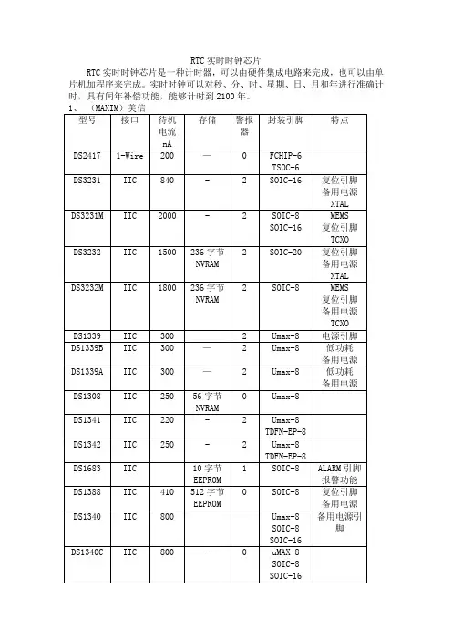
RTC实时时钟芯片RTC实时时钟芯片是一种计时器,可以由硬件集成电路来完成,也可以由单片机加程序来完成。
实时时钟可以对秒、分、时、星期、日、月和年进行准确计时,具有闰年补偿功能,能够计时到2100年。
消费类电子(机顶盒、VCR),手持式装置(GPS、POS终端),医疗设备,办公设备,电信(路由器、交换机、服务器),电器设备,汽车,消费类电子,嵌入式时标,工业,电表。
DS3231集成了温度补偿晶体振荡器(TCXO)和晶体,电池备份输入用于支持连续计时,可编程方波输出,低电平有效复位输出。
关键参数:工作温度商业级:0°C至+70°C,具有2ppm精度;工业级:40°C至+85°C,具有3.5pmm精度。
DS3231M是业内首款内置MEMS、带温度补偿的RTC,允许器件用于强烈震动的场合,不会由于晶体失效而导致产品故障。
DS3232相比较于DS3231将32kHz输出驱动器更改为推挽输出,省去一个外部上拉电阻,节省空间,够加快时钟的边沿速度,降低器件功耗。
电池切换时,可通过32kHz位选择使能/禁止32kHz输出。
DS3232的32kHz输出在关闭状态下驱动至低电平,DS3231的32kHz输出在关闭状态下为高阻输出。
DS3232内部可通过2个CRATE位控制温度转换速率,这些位用于控制器件的采样率。
采样率决定了对温度传感器进行数字转换的频率,以及补偿振荡器的时间间隔。
降低采样率则降低了温度传感器的工作频率,从而降低整体功耗。
此外,DS3232具有236字节的SRAM。
压检测功能和振荡停止检测功能,内置定时器可以产生周期性的定时中断信号,警报器用于定时报警,可设定天、日期、小时、分钟。
工作电压范围:1.70V-5.5V。
计时保持电压:1.15V-5.5V。
此外,采用IIC接口,支持低功耗模式。
RX6110频率输出功能:能选择输出频率,有32.768kHz, 1024Hz, 1Hz。

AMI8563AMI8563I2C 实时时钟/日历芯片1.概述AMI8563 是低功耗的CMOS 实时时钟/日历芯片,它提供一个可编程时钟输出,一个中断输出和掉电检测器,所有的地址和数据通过I2C总线接口串行传递。
最大总线速度为400Kbits/s,每次读写数据后,内嵌的字地址寄存器会自动产生增量。
2.特性* 低工作电流:典型值为0.25µA(V DD=3.0V,Tamb=25℃时)。
* 世纪标志* 大工作电压范围:1.0~5.5* 低休眠电流;典型值为0.25µA(V DD=3.0V,Tamb=25℃)* 400KHz 的I2C 总线接口(V DD=1.8~5.5V 时)。
* 可编程时钟输出频率为:32.768KHz,1024Hz,32Hz,1Hz。
* 报警和定时器。
* 掉电检测器。
* 内部集成的振荡器电容。
* 片内电源复位功能。
* I2C 总线从地址:读,0A3H;写,0A2H。
* 开漏中断引脚。
3.应用* 复费率电度表、IC卡水表、IC卡煤气表* 移动电话* 便携仪器* 传真机AMI8563* 电池电源产品4.简明参考数据表1 简明参考数据符号 描述 条件 最小值 最大值 单位I2C 总线无效; Tamb =25℃1.0 5.5 VV DD工作电压I2C 总线有效; fSCL=400kHz Tamb=-40~+85℃1.8 5.5 V VfSCL=400kHz — 800 μAfSCL=100kHz — 200 200 µA fSCL=0Hz ; Tamb =25℃VDD=5V — 550 nA I DD工作电流;定时器和 CLKOUT 失效VDD=2V — 450 nATamb 工作温度范围 -40 +85 ℃ Tstg 储存温度 -65 +150 ℃5.订单信息表2 订定单信息包装型号名称描述版本AMI8563P DIP8 塑料双列直插式封装;8 脚(300mil) SOT97-1 AMI8563T SO8 小塑料封装;8 脚;宽3.9mm SOT96-1 AMI8563TS TSSOP8 小塑料薄型封装;8 脚;宽3.0mm SOT505-1AMI8563 6.方框图图1 方框图7.管脚配置7.1 管脚图2 管脚配置AMI8563图3二极管保护图7.2 管脚描述符号管脚号描述OSCI 1 振荡器输入OSCO 2 振荡器输出中断输出(开漏;低电平有效)/INT 3VSS 4 地SDA 5 串行数据I/OSCL 6 串行时钟输入CLKOUT 7 时钟输出(开漏)VDD 8 正电源8. 功能描述AMI8563 有16 个8位寄存器:一个可自动增量的地址寄存器,一个内置32.768KHz 的振荡器(带有一个内部集成的电容),一个分频器(用于给实时时钟RTC 提供源时钟),一个可编程时钟输出,一个定时器,一个报警器,一个掉电检测器和一个400KHz I2C总线接口。
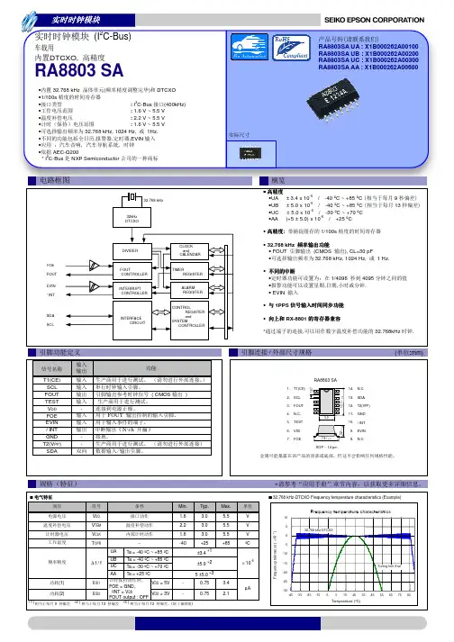
实际尺寸电路框图概览引脚功能定义引脚连接 / 外部尺寸规格(单位:mm)规格(特征)*请参考“应用手册”章节内容,以获取更多详细信息。
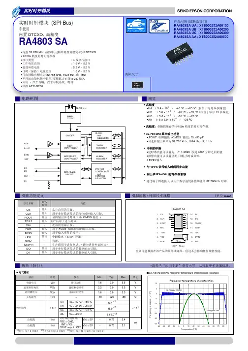
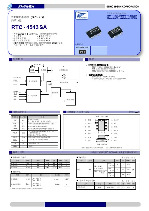
RTC-4543SA实时时钟模块 (SPI-Bus)简单功能 RTC - 4543 SA∙内置32.768 kHz 晶体单元. (频率精度调整完毕) ∙接口类型 :3线串行接口 ∙工作电压范围 :2.5 V ~ 5.5 V ∙宽计时器电压范围 :1.4 V ~ 5.5 V ∙32.768 kHz 频率输出功能 :带控制引脚的CMOS 输出 ∙包括时刻、日历、电压检测功能等产品号码(请联系我们)RTC-4543SA : Q41454352000200 RTC-4543SB : Q41454361000200推进环境管理体系 符合国际标准在环境管理体系的运行方面,使用ISO14001国际环境标准,通过“计划-实施-检查-验证(PDCA)的循环来实现持续改进。
公司位于日本和海外的主要制造基地已取得了ISO14001资格认证。
追求高品质Seiko Epson 为了向顾客提供高品质、卓越信赖性的产品、服务,迅速着手通过ISO 9000系列资格认证的工作,其日本和海外工厂也在通过ISO 9001认证。
同时,也在通过大型汽车制造厂商要求规格的ISO/TS 16949认证。
关于在目录内使用的记号●无铅。
●符合欧盟RoHS 指令。
欧盟RoHS 指令免检的含铅产品。
(密封玻璃、高温熔化性焊料或其他材料中包含铅。
)●为汽车方面的应用,如汽车多媒体、车身电子、遥控无钥门锁等。
●为汽车行驶安全方面的应用(引擎控制单元、气囊、电子稳定程序控制系统)。
注意事项·本材料如有变更,恕不另行通知。
量产设计时请确认最新信息。
·未经Seiko Epson 公司书面授权,禁止以任何形式或任何方式复制或者发布本材料中任何部分的信息内容。
·本材料中的书面信息、应用电路、编程、使用等内容仅供参考。
PCF8563实时时钟/日历第11版——2015年10月26日产品数据手册1. 简介PCF8563是一款低功耗的CMOS1实时时钟/日历芯片,支持可编程时钟输出、中断输出和低压检测。
所有地址和数据通过双线双向I2C总线串联传输,最高速率:400 kbps。
每次读写数据字节后,寄存器地址自动累加。
2. 特性和优势◼基于32.768kHz的晶振,提供年、月、日、星期、时、分和秒计时◼Century flag◼时钟工作电压:1.0 - 5.5 V(室温)◼低备用电流;典型值为0.25 μA(V DD = 3.0 V,T amb =25 °C)◼400 kHz 双线I2C总线接口(V DD = 1.8 - 5.5 V)◼可编程时钟输出(32.768 kHz、1.024 kHz、32 Hz和1Hz)◼报警和定时器功能◼集成晶振电容器◼内部上电复位(POR)◼I2C总线从机地址:读:A3h;写:A2h◼开漏中断管脚3. 应用◼移动电话◼便携式仪器◼电子计量◼电池驱动产品1. 有关本资料表所使用的缩略语及首字母缩略语的定义,请参考第18节。
4. 订购信息表1. 订购信息[1] 不推荐用于新产品设计。
替代零件为PCF8563T/5。
[2] 不推荐用于新产品设计。
替代零件为PCF8563TS/5。
5. 标示表2. 标记代码6. 功能框图图1. PCF8563功能框图7. 引脚配置信息7.1 引脚配置图2. HVSON10的引脚配置(PCF8563BS) 图3. SO8的引脚配置(PCF8563T)图4. TSSOP8的引脚配置(PCF8563TS)7.2 引脚说明表3. 引脚说明[1] 晶粒芯片焊盘(外露式焊盘)通过高电阻(非导电的)芯片附着连接到VSS,并应进行电气隔离。
将外露式焊盘焊接到电气隔离的PCB铜焊盘上,以获得更好的传热效果,这是一种较好的工程实践,但由于RTC不会消耗太多功率,因此并不需要这样做。
HYM1302HYM8563I 2C 实时时钟/日历芯片钟 特 点■ 可计时基于32.768kHz 晶体的秒,分,小时,星期,天,月和年 ■ 带有世纪标志■ 宽工作电压范围:2.0~5.5V■ 低休眠电流:典型值为0.25μA(V DD =3.0V,T A =25℃)■ I 2C总线从地址:读,0A3H;写,0A2H■ 可编程时钟输出频率为:32.768kHz,1024Hz,32Hz,1Hz ■ 报警和定时器 ■ 掉电检测器 ■ 内部集成振荡电容■ 封装形式:DIP8、SOP8和MSOP8 ■ 漏极开路中断引脚应 用■ 便携仪器 ■ 移动电话 ■ 复费率电度表、IC 卡水表、IC 卡煤气表 ■ 传真机■ 门禁概述HYM8563是一款低功耗CMOS实时时钟/日历芯片,它提供一个可编程的时钟输出,一个中断输出和一个掉电检测器,所有的地址和数据都通过I 2C总线接口串行传递。
最大总线速度为400Kbits/s,每次读写数据后,内嵌的字地址寄存器会自动递增。
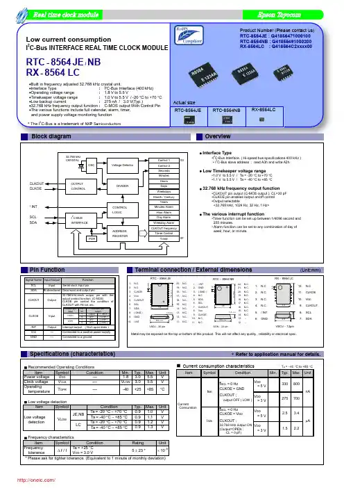
方框图和管脚功能图1.方框图管脚说明管脚序号符号 功能描述管脚序号符号 功能描述1 OSCI 振荡器输入 5 SDA 串行数据I/O2 OSCO振荡器输出 6 SCL 串行时钟输入 3中断输出(开漏) 7 CLKOUT 时钟输出(开漏) 4V SS 地8V DD正电源最大额定值参数符号 最小值最大值单位电源电压 V DD -0.5 +6.5 V 电源电流I DD-50 +50 mASCL 和SDA 管脚输入电压 -0.5 +6.5 VOSCI 管脚输入电压 V I-0.5 V DD +0.5 V CLKOUT 和 管脚输出电压 V O -0.5 +6.5 V 所有输入口的直流输入电流 I I -10 +10 mA 所有输出口的直流输出电流 I O -10 +10 mA 总损耗功率 P — 300 mW工作温度 T A -40 +85 ℃ 贮存温度 T S-65 +150 ℃电气特性参数直流电特性(如无特别说明,V DD =1.8~5.5V ,V SS =0V ;T A =-40~+85℃;f osc =32.768kHz;石英晶片Rs=40kΩ,C L =8pF)参数符号 测试条件 最小值典型值 最大值 单位电源 I 2C 总线失效,T A = 25℃[1] 1.8 - 5.5 V 工作电压I 2C 总线有效,f=400kHz [1]2.0 - 5.5 V 提供可靠的时钟/日历数据时的工作电压V DDT A =25℃ V low - 5.5 VCLKOUT 有效(FE=1)f SCL =100kHz - - 200 µAf SCL =0Hz ,T A = 25℃[2]V DD =5.0V- 275 550 nA V DD =3.0V- 250 500 nA V DD =2.0V- 225 450 nA f SCL =0Hz ,T A = -40~+85℃[2]V DD =5.0V - 500 750 nA V DD =3.0V - 400 650 nA 工作电流2 CLKOUT 禁止 (FE=0)I DD2V DD =2.0V- 400 600 nA f SCL =0Hz ,T A = 25℃[2]V DD =5.0V - 825 1600 nA V DD =3.0V- 550 1000 nA V DD =2.0V- 425 800 nA f SCL =0Hz ,T A = -40~+85℃[2]V DD =5.0V - 950 1700 nA V DD =3.0V - 650 1100 nA 工作电流3CLKOUT=32.768kHzI DD3V DD =2.0V- 500 900 nA 输入低电平输入电压 V IL V SS- 0.3V DD V 高电平输入电压 V IH 0.7V DD-V DDV输入漏电流 I LI V I =V DD 或V SS-1 0 +1 µA输入电容 C I [3]-- 8 pF输出SDA 低电平输出电流 I OLS V OL =0.4V ,V DD =5.0V -3 - - m A 低电平输出电流 I OLI V OL =0.4V ,V DD =5.0V -1 - - m A CLKOUT 低电平输出电流I OLC V OL =0.4V ,V DD =5.0V -1 - - m A CLKOUT 高电平输出电流I OHC V OL =4.6V ,V DD =5.0V 1 --m A输出漏电流 I LOVO=V DD 或V SS-1 0 +1 µA电压检测器 掉电检测电压V LOWT A = 25℃- 0.9 1.0 V1、加电时振荡器可靠起动:V DD (最小值,加电时)= V DD (最小值)+0.3V2、定时器源时钟=1/60Hz ;SCL 和SDA 都为V DD3、在样品基础上测试交流特性(如无特别说明,V DD =1.8~5.5V ,V SS =0V ;T A =-40~+85℃;f osc =32.768kHz;石英晶体Rs=40kΩ,C L =8pF)参数符号测试条件最小值典型值最大值 单位振荡器精确负载电容 C INT15 25 35 pF 振荡器稳定性Δf OSC /f OSCΔV DD =200mV,T A =25℃-2×10⁻⁷--石英晶体参数(f=32.768kHz )串联电阻 R S -- 40 k Ω微调电容C T 5- 25 pF CLKOUT输出CLKOUT占空因数δCLKOUT[1]- 50 - % I2C总线定时特性[2] [3]SCL时钟周期f SCL[4]-- 400 kHz 起动条件保持时间t HDSTA 0.6--µs重复起动条件建立时间t SUSTA 0.6--µsSCL低电平时间t LOW 1.3--µs SCL高电平时间t HIGH 0.6--µsSCL和SDA的上升沿时间t r-- 0.3 µsSCL和SDA的下降沿时间t f-- 0.3 µs 总线负载电容C b-- 400 pF 数据建立时间t SUDAT 100-- ns 数据保持时间t HDDAT 0-- ns 停止条件建立时间t SUSTO 0.6--µs可接受的总线尖峰宽度t SW-- 50 ns1、无特别说明f CLKOUT = 32.768kHz2、所有定时数值在工作电压范围内(T A条件下)有效,参考输入电压V SS到V DD之间变化是V IL和V IH的值3、I2C总线在两个起动和一个停止条件下的访问时间必须小于1s功能描述HYM8563有16个8位寄存器,一个可自动增量的地址寄存器,一个内置32.768kHz振荡器(带有一个内部集成的电容),一个分频器(用于给实时时钟RTC提供时钟源),一个可编程时钟输出,一个定时器,一个报警器,一个掉电检测器和一个400kHz的I2C总线接口。
SPXO SG-3030CMProduct nameSG-3030CM 32.768000 kHz B Product Number / Ordering code X1B0002110001xxPlease refer to the 8.Packing information about xx (last 2 digits)Output waveform CMOSPb free / Complies with EU RoHS directiveReference weight Typ. 13 mg1.Absolute maximum ratings ParameterSymbolMin.Typ.Max.UnitConditions / RemarksMaximum supply voltage Vcc-GND -0.3-7V Vcc PinStorage temperatureT_stg-55-125ºCStorage as single product2.Specifications(characteristics)ParameterSymbolMin.Typ.Max.UnitConditions / RemarksOutput frequencyf0-32.7680-kHz Supply voltageVcc 1.5- 5.5V Vcc Pin Interface power supply voltage V IO 1.5- 5.5VIO PinOperating temperatureT_use -40-85ºC No condensationFrequency tolerancef_tol -18-28x10-6@+25℃, Vcc=3.3V , 5+/-23x10^-6Frequency temperature coefficient f0-Tc -120-10x10-6-20℃ to 70℃ (+25℃ is reference)Frequency voltage coefficient f0-Vcc -2-2x10⁻⁶ /V `@+25℃ Vcc=1.5V to 5.5V Current consumption Icc --2μA Vcc=3.3V No load condition Symmetry SYM 455055%1/2Vcc(VIO )Level Output voltage V OH VIO-0.4--IOH=-400μA V OL --GND+0.4IOL=400μAOutput load condition L_CMOS --15pFCMOS Load Input voltage V IH 80%Vcc---V IL--20%Vcc -Rise time t r --200ns Fall time tf --200ns Start-up time t_str --1sVcc=2.0V to 5.0VFrequency agingf_age-5-5x10⁻⁶@+25℃ Vcc=3.3V First year3.Timing chart20%VIO ⇔ 80%VIO 15pF VIO=1.5V to 5.5V 20%VIO ⇔ 80%VIO 15pF VIO=1.8V to 5.5VGNDV CC tr 50 %V CCttw80 %V CC20 %V CC tf4.Test circuit1) Waveform observation 2) Current consumption*Current consumption under the disable function should be = GND.3) Condition (1) Oscilloscope· Band width should be minimum 5 times higher (wider) than measurement frequency.· Probe earth should be placed closely from test point and lead length should be as short as possible.* Recommendable to use miniature socket. (Don’t use earth lead.)(2) L_CMOS also includes probe capacitance.(3) By-pass capacitor (0.01 mF to 0.1 mF) is placed closely between VCC and GND.(4) Use the current meter whose internal impedance value is small.(5) Power supply· Start up time (0 %VCC ® 90 %VCC) of power source should be more than 150 ms.· Impedance of power supply should be as lowest as possible.V CCSTOUTGNDswichsupplyby-pass capacitorTest PointAor OEor OEV CCSTOUTGNDsupplyby-passcapacitorL_CMOSTest Point5.External dimensions (Unit: mm)6.Footprint(Recommended) (Unit: mm)7.Reflow profileReflow condition (Follow of JEDEC STD-020D.01)8.Packing information[ 1 ]Product number last 2 digits code(xx) descriptionThe recommended code is "00"X1B0002110001xxCode Code 01Any Q'ty vinyl bag(Tape cut)141000pcs / Reel 11Any Q'ty / Reel 152000pcs / Reel 12250pcs / Reel003000pcs / ReelConditionConditionTemperature [ ︒C ] 60 300 250200 150 100 50ts60 s to 180 s( +150 ︒C to +200 ︒C )Avg. Ramp-up 3 ︒C / s Max.Ramp-down 6 ︒C / s Max.Time [ s ]120 180 240 300 360 420 480 540 600 660 720 780Ts min ; +150 ︒CTs max ; +200 ︒C TL; +217 ︒C+255 ︒CtL60 s to 150 s( +217 ︒C over )tp ; 20 s to 40 sTP ; +260 ︒C Time +25 ︒C to Peak3.2±0.22.351.5±0.2#2 #1 #2#4#30.9 M a x .#30.65 0.5#1#40.4Pin mapPin Connection 1 V IO 2 GND 3 OUT 4 V CC3030 ○B123B1.052.651.20.8[ 2 ] Taping specificationSubject to EIA-481 & IEC-60286(1) Tape dimensions Material of the Carrier Tape : PS Material of the Top Tape : PET+PEUnit: mm(2) Reel dimensionsCenter material : PS Material of the Reel : PSφ1.0 ±0.1+0.14.0±0.12.0±0.054.0±0.110P: 40±0.15.5±0.05+0.312.0-0.11.75±0.13.6±0.10.3±0.051.0±0.11.9±0.1TopG 穴Φ76 mmΦ160 mmH Φ3Φ180 mm +015.40±1 mm13.00±0.3 mmΦ60 mmΦ21±0.8 mmΦ13±0.2 mm2.00 mm +0.39.Notice·This material is subject to change without notice.·Any part of this material may not be reproduced or duplicated in any form or any means without the written permission of Seiko Epson.·The information about applied data,circuitry, software, usage, etc. written in this material is intended for reference only.Seiko Epson does not assume any liability for the occurrence of customer damage or infringing on any patent or copyright of a third party.This material does not authorize the licensing for any patent or intellectual copyrights.·When exporting the products or technology described in this material, you should comply with the applicable export control laws and regulations and follow the procedures required by such laws and regulations.·You are requested not to use the products (and any technical information furnished, if any) for the development and/or manufacture of weapon of mass destruction or for other military purposes. You are also requested that youwould not make the products available to any third party who may use the products for such prohibitedpurposes.·These products are intended for general use in electronic equipment. When using them in specific applications that requireextremely high reliability, such as the applications stated below, you must obtain permission from Seiko Epson in advance./ Space equipment (artificial satellites, rockets, etc.)/ Transportation vehicles and related (automobiles, aircraft, trains, vessels, etc.)/ Medical instruments to sustain life/ Submarine transmitters/ Power stations and related/ Fire work equipment and security equipment/ Traffic control equipment/ And others requiring equivalent reliability.。
使用说明书版权所有。
没有精工爱普生株式会社的正式书面许可,本手册不得复制,不得保存在可再生系统内,或以任何形式任何手段进行电子、机械转载、复印、录制等。
使用本手册内的有关信息无须授权。
在编辑本手册时我们考虑到了各项防备措施,对于手册中的错误和遗漏,精工爱普生株式会社概不负责。
同时,也不负责由于使用本手册中的信息内容造成的损失。
本产品由于用户或第三方造成的事故、错误使用和乱用,以及擅自改装、修理或变更式样等,不严格遵守精工爱普生株式会社的操作和维修要求(美国除外),引起的危害、损失、费用和付出款项等,不论是精工爱普生株式会社还是其它有关的集团公司,对于该顾客或第三方概不负有任何责任。
由于使用非正规爱普生产品或非精工爱普生株式会社指定许可的任何附件或任何消耗品,从而造成的损失和故障,精工爱普生株式会社概不负责。
EPSON 以及ESC/POS 是精工爱普生株式会社的注册商标。
备注:本手册中的内容有可能发生更改,恕不事先通知。
版权所有者©2007精工爱普生株式会社,长野,日本应用安全标准该产品遵守以下标准。
如发生不合乎这些标准的情况时,请与销售商联系。
EMC: GB9254GB17625.1安全 : GB4943安全防范这一部分介绍有关确保本产品的安全和有效使用的重要信息。
请仔细阅读此部分并将其保存在便于拿到的地方。
警告:❏如果发生冒烟、异常气味、或者不正常的噪音时,请立即关闭机器。
继续使用可能会引起火灾。
应该立即拔掉插头,并与销售商或精工爱普生服务中心取得联系询问处理办法。
❏请勿试图自行维修本机。
不正确的维修是很危险的。
❏请勿自行拆卸或校正。
不正确的动作会对本机造成伤害或火灾。
❏请使用符合规格的电源。
连接不符合规格的电源可能会导致火灾。
❏防止任何异物落入机内,以免引起火灾。
❏如果有水或其他液体流入机内,请立即拔掉电源线,并且与销售商或精工爱普生服务中心取得联系询问处理办法。
继续使用可能会导致火灾。