厚生电阻规格书 兴泰隆
- 格式:pdf
- 大小:375.88 KB
- 文档页数:13
Page-1Approval SheetforCarbon Film ResistorsCFR series±2% & ±5%YAGEO CORPORATIONHeadquarters: 3F, No.233-1, Pao Chiao Rd., Shin Tien, Taipei, Taiwan,R.O.C.Tel: 886-2-2917-7555 Fax: 886-2-2917-4286URL: Page-2Page-31. PRODUCT : CARBON FILM RESISTORS(Normal & Miniature Style)2. PART NUMBER : Part number of the carbon film resistor is identified by the name,power, tolerance, packing, temperature coefficient, special type and resistance value.Example :CFR -12 J T J 52 100RSeries Size Resistance Packing Temperature Special ResistanceName Code Tolerance Style Coefficient Type Value of Resistance(1) Style: CFR SERIES(2) Power Rating: -12=1/6W 、25S=1/4WS 、-25=1/4W 、50S=1/2WS 、-50=1/2W 、 1WS=1WS 、100=1W 、2WS=2WS 、200=2W(3) Tolerance: G=±2% J=±5%(4) Packaging Type : R =Paper Taping Reel T =Tape on Box Packing B =Bulk Packing(5) T .C .R : J=±350ppm/℃ — =lgnore(6) Special Type : 26=26mm 、52=52.4mm 、73=73mm 、 PN =PANAsert AV =AVlsert(7) Resistance Value: 1R 、10R 、100R 、10K 、100K 、330K 、1M………Page-43. BAND-CODE:4. ELECTRICAL CHARACTERISTICSTabe I*Standard resistance is 1Ω~ 10M Ω, below or over this resistance on request. *Rated Continuous Working Voltage (RCWV)=Value Resistance Rating Power ×FIG.1 TEMPERATURE COEFFICIENTPage-55. DERATING CURVE & HOT-SPOT TEMPERATURE6. DIMENSIONS7. ENVIRONMENTAL CHARACTERISTICS(1) Short Time Over Load TestAt 2.5 times of the rated voltage. (If the voltage exceeds the maximum load voltage, the maximum load voltage will be used as the rated voltage) applied for 5 seconds, the resistor should be free from defects after the resistor is released from load for about 30 minutes and the change of the resistance value should be within ±(0.25%+0.05Ω) as compared with the value before the test.Page-6(2) Dielectric Withstanding VoltageThe resistor is placed on the metal V Block. Apply a Table I dielectric withstanding between the terminals connected together with the block for about 60 seconds. The resistor shall be able to withstand without breakdown or flashover.(3) Temperature Coefficient TestTest of resistors above room temperature 125°C to 130°C (Testing Temperature) at the constant temperature silicon plate for over 4 to 5 minutes. Then measure the resistance. The Temperature Coefficient is calculated by the following equation and its value should be within the range of requested.600010t t 1R R R t Coefficien e Temperatur sistor Re ×−×−=R= Resistance value under the testing temperature R 0= Resistance value at the room temperature t = The testing temperature t o = Room temperature(4) Insulation ResistanceApply test terminal on lead and resistor body. The test resistance should be high than 10,000 Mohm.(5) SolderabilityImmerse the specimen into the solder pot at 230±5°C for 5±0.5 seconds. At least 95% solder coverage on the termination.(6) Resistance to SolventThe specimen into the appropriate solvent of Methyleme Chloride condition ofultrasonic machine for 1 minutes. The specimen is no deterioration of coatings and color code.(7) Terminal StrengthDirect Load – Resistors shall be held by one terminal and the load shall be gradually applied in the direction of the longitudinal axis of the resistor unit the applied load reacheds 5 pounds. The load shall be held for 10 seconds. The load of weight shall be ≧2.5kg(24.5N).Page-7(8) Pulse OverloadApply 4 times of rated voltage to the specimen at the 1 second on and 25 seconds off cycle, subjected to voltage application cycles specified in 10000. The change of the resistance value shall be within ±(2%+0.05Ω).(9) Load Life in HumidityPlace the specimen in a test chamber at 40±2°C and 90~95% relative humidity. Apply the rated voltage to the specimen at the 1.5 hours on and 0.5 hour off cycle. The total length of test is 1000 hours. The change of the resistance value shall be within ±(1.5%+0.05Ω).(10) Load Life TestPlaced in the constant temperature chamber of 70±3°C the resistor shall be connected to the lead wire at the point of 25mm. Length with each terminal, the resistors shall be arranged not much effected mutually by the temperature of the resistors and the excessive ventilation shall not be performed, for 90 minutes on and 30 minutes off under this condition the rated D.C. voltage is applied continuously for 1000+48/-0 hours then left at no-load for 1hour, the change of the resistance value measured at this time to the value before the test shall be within ±(1.5%+0.05Ω). There shall be no remarkable change in the appearance and the color code shall be legible after the test.(11) Temperature Cycling TestThe temperature cycle shown in the following table shall be repeated 5 times consecutively. The measurement of the resistance value is done before the first cycle and after ending the fifth cycle, leaving in the room temperature for about 1 hour, the change shall be within ±(1%+0.05Ω). After the test the resistor shall be free from the electrical or mechanical damage.Temperature Cycling Conditions: Step Temperature(°C) Time (minute)1 +25+10 -5 10 to152 -65+0 -3 30 3 +25+10 -5 10 to15 4+150+3 -030Page-8(12) Resistance to Soldering HeatThe terminal lead shall be dipped into the solder pot at 350±10°C for 3±0.5 seconds up to 3 mm. The change of the resistance value shall be within ±(1%+0.05Ω).8. PACKING METHODS Bandolier for Axial leadsThe resistors are supplied on bandolier, either 1000 resistors in ammopack or 5000 resistors on reel.9. TAPE ON REEL PACKING & TAPE ON BOX PACKING10. SPECIAL TYPE (FORMING DIMENSIONS)。
Page 4•Small size and lightweight• Suitable for both flow and reflow soldering •Reduction of assembly costs and matching with placement machines2007 - 2008Standard: 2%, 5%, 10%---E 24 series 1%---E 96 series2007 - 2008 Page 5Marking on the Resistors Body:•For 0402 size, no marking on the body due to the small size of the resistor.•±5% tolerance product. (Including resistance values less than 1Ω; both 1% and 5%) The marking is 3 digits, the first 2 digits are the significant figures of the resistance and the 3rd digit denotes number of zeros.153 = 15000Ω = 15KΩ; 120 = 12Ω Below 10Ω shown as this: 6R8 = 6.8Ω 0.1Ω~0.99Ω shown as this: R33 = 0.33Ω•±1% tolerance marking of case size 0805 and bigger is 4 digits, the first 3 digits are the significant figures of the resistance and the 4th digit denotes number of zeros.2372 = 23700Ω = 23.7KΩ; 1430 = 143Ω Below 10Ω shown as this: 3R24 = 3.24Ω0.1Ω~0.99Ω shown as this: R33 = 0.33ΩPage 62007 - 2008* More details, please see pages 78-79.• Standard E-96 series values (±1% tolerance) of 0603 size. Due to the small size of the resistor’s body, 3 digitsmarking will be used to indicate the accurate resistance value by using the Multiplier code & Standard E-96 Series Resistance Value Code as shown on Page 6.1.96K Ω = 196 x 101 Ω = 29B12.4Ω = 124 x 10-1 Ω = 10X• Standard E-24 series values which does not belong to E-96 series values (in ±1% tolerance) of 0603 size. The marking is the same as 5% tolerance but marked with underline.122 = 1200 = 1.2K Ω680 = 68ΩTemperature coefficient±5%: 1Ω ~ 10M Ω ≤ ±200PPM/°C±1%: 10Ω ~ 100Ω ≤ ±200PPM/°C; 101Ω ~ 1M Ω ≤ ±100PPM/°C Short-time overload ±5%: ±(2.0% + 0.1Ω) Max. ±1%: ±(1.0% + 0.1Ω) Max. Insulation resistanceMin. 1,000 Mega OhmDielectric withstanding voltageNo evidence of flashover, mechanical damage, arcing or insulation breakdown Terminal bending ±(1.0% + 0.05Ω) Max.Soldering heat Resistance change rate is ±(1.0% + 0.05Ω) Max. SolderabilityMin. 95% coverage Temperature cycling ±5%: ±(1.0% + 0.05Ω) Max. ±1%: ±(0.5% + 0.05Ω) Max. Humidity (Steady State) ±5%: ±(3.0% + 0.1Ω) Max. ±1%: ±(0.5% + 0.1Ω) Max. Load life in humidity±5%: ±(3.0% + 0.1Ω) Max. ±1%: ±(1.0% + 0.1Ω) Max. Load life±5%: ±(3.0% + 0.1Ω) Max.±1%: ±(1.0% + 0.1Ω) Max.* The values which are not of standard E-24 series (2% & 5%) and not of E-96 series (1%) could be offered on a case to case basis.2007 - 2008Page 72007 - 2008Page 8•16P8 (16Pin 8R)THICK FILM CHIP RESISTOR ARRAYS• High density 2, 4, 8 resistors in one small case (convex type) • Improvement of placement efficiency• Packaging is suitable for automatic placement machines • Superior solderability • Scalloped•2D02 (4Pin 2R)•4D02, 4D03 (8Pin 4R)•10P8 (10Pin 8R)Part No.StyleLWHℓ1ℓ2PQ2D02 (0402x2) 2D02 (4Pin 2R) 1.0 ± 0.1 1.0 ± 0.1 0.35 ± 0.1 0.17 ± 0.1 0.25 ± 0.1 0.65 ± 0.05 0.33 ± 0.1 4D02 (0402x4) 4D02 (8Pin 4R) 2.0 ± 0.1 1.0 ± 0.1 0.45 ± 0.1 0.2 ± 0.15 0.3 ± 0.15 0.5 ± 0.05 0.3 ± 0.05 4D03 (0603x4) 4D03 (8Pin 4R) 3.2 ± 0.2 1.6 ± 0.2 0.5 ± 0.1 0.3 ± 0.15 0.3 ± 0.15 0.8 ± 0.1 0.5 ± 0.15 16P8 16P8 (16Pin 8R) 4.0 ± 0.2 1.6 ± 0.15 0.45 ± 0.1 0.3 ± 0.15 0.4 ± 0.15 0.5 ± 0.05 0.3 ± 0.05 10P8 10P8 (10Pin 8R)3.2 ± 0.21.6 ± 0.150.55 ± 0.10.4 ± 0.10.3 ± 0.150.64 ± 0.050.35 ± 0.05Resistance RangePart No. StylePower Rating at 70ºC Max. Working Voltage Max. Overload VoltageDielectric With-standing VoltageOperated Temp. RangeF (±1%) E-96 seriesJ (±5%) E-24 seriesJumper Rated Current2D02 2D02 (4Pin2R) 1/16W 50V 100V 500V -55ºC~+155ºC - 10Ω~ 1M Ω - 4D02 4D02 (8Pin4R) 1/16W 50V 100V 500V -55ºC~+155ºC -10Ω~ 1M Ω -4D03 4D03 (8Pin4R) 1/16W 50V 100V 500V -55ºC~+155ºC 100Ω~560K Ω 10Ω~ 1M Ω 1A 16P8 16P8 (16Pin8R) 1/16W 50V 100V 100V -55ºC~+155ºC - 10Ω~ 1M Ω - 10P810P8 (10Pin8R)1/32W 25V 50V 50V -55ºC~+155ºC -33Ω~ 100K Ω -Note: Part number and ordering procedure the same as Thick Film Chip Resistors on Page 4.Standard: 2%, 5%, 10%---E 24 series 1%---E 96 series。
UniOhm Uniroyal Electronics Industry Co., Ltd.厚声电子工业有限公司88 LongTeng Road, Economic & Technical Development Zone,Kunshan City, Jiangsu, China中国江苏省昆山市经济技术开发区龙腾路88号邮编: 215301Tel: +86 512 5763 1400 / 1411 /1422 /1433Fax: +86 512 5763 4599*******************************************Contents目录Metal Strip Current Sensing Chip Resistors - MS 金属带电流检测片式电阻器22MS06, MS07, MS10, MS11, MS12, MS17, MS20, MS27Anti-Electro Static Discharge Thick Film Chip Resistors - ES 抗静电膜晶片电阻器24ES01, ES02, ES03, ES05, ES06, ES07Low T.C.R Thick Film Chip Resistors - LT 低温度系数厚膜晶片电阻器26LT02, LT03, LT05, LT06AEC-Q200 Version Chip Resistors - HQ 汽车用晶片电阻器28HQ02, HQ03, HQ05, HQ06, HQ07, HQ10 , HQ12Thick Film Chip Resistors Network 厚膜晶片网络电阻器4610P8, 10S8, 10T8, 10E9Packing of Surface Mount Resistors 表面贴装式电阻器包装47Packing of Surface Mount ResistorsResistor Network - SIP Series 网络电阻器 - SIP 系列48RNL-A, RNL-B, RNL-C, RNL-D, RNL-E, RNL-L, RNL-R,RNL-G, RNL-PHigh Power Resistor Network - SIP RPL Series 高功率网络电阻器- SIP RPL 系列50RPL-A, RPL-B, RPL-RHigh Power Resistors Network Medium Profile–SIP RNM Series高功率中宽度网络电阻器 - SIP RNM 系列52RNM-A, RNM-B, RNM-RHigh Power Resistors Network High Profile–SIP RPH Series高功率高宽度网络电阻器 - SIP RPH 系列54RPH-A, RPH-B, RPH-RSpecial Network –SIP Series 特殊网络电阻器 - SIP 系列56SN0001, SN0002, SN0003, SN0004Resistor/Capacitor Network-SIP Series 网络阻容器电阻器 - SIP 系列57RCN-A, RCN-BCapacitor Network-SIP Series 网络电容器 - SIP 系列58CNM-1High Voltage Flat Resistors 高压扁平式电阻器59HFRCarbon Film Fixed Resistors 碳膜电阻器60CFRPrecision Metal Film Fixed Resistors 精密金属膜电阻器62MFRCarbon Film Power Resistors 高功率碳膜电阻器64CPR Metal Film Power Resistors 高功率金属膜电阻器65MPRWire-wound Fusible Resistors 绕线保险丝型电阻器74KFRThermal Fusing Wire-wound Fixed Resistors 绕线型温度保险丝电阻器76TFRCurrent Sense Resistors 电流检测线电阻器77CSRCurrent Sense Spring Resistors 弹簧式电流检测电阻器78CSSA, CSSB, CSSCThrough Hole Category - Network Resistors & Traditional Coated Resistors (插件式 - 排列电阻 & 涂装型电阻)New New New New UniOhm1Contents目录Axial Leaded Terminal Type-PRW Series 轴式导线型 - PRW 系列 97PRW , PRWA, PRWCRadial Leaded T ype-PRM & PRS Series 立式导线型 - PRM & PRS 系列 98PRM, PRMA, PRMB, PRMT , PRSUltra-Low Value Cement Resistors 超低阻水泥固定电阻器108PRWUPower Flat Alloy Resistors 功率型合金箔电阻器109PFAS, PFATColumnar Type Cement Fixed Resistors 圆柱状水泥电阻器111QHOStandard Packing of Cement Type Resistors 水泥型电阻器包装标准112Bulk/BoxPower Dissipation Mount Resistors 铝外壳电阻器115PDMHigh-Power Wire-wound Resistors 高功率绕线型固定电阻器116BTRVitreous Enameled Wire-wound Resistors 珐琅釉绕线固定电阻器127URXPower Type Thermal Fusing Resistors 功率型温度保险丝电阻128TFO, TFRCPower (Ribbon) Wire-wound Resistors 功率(合金带)绕线型电阻器129QH, QL, QR, QRZGTest Method of JIS-C-5201 & JIS-C-5202JIS-C-5201和 JIS-C-5202 检测方法131Standard Nominal Resistance Value 标准电阻值133Explnation of Part No. System 料号系统注释135Standard Color Code System 标准色码系统137Metal Glaze Film Fixed Resistors 金属玻璃釉膜固定电阻器79MGRHigh-Value Metal Glaze Film Fixed Resistors 超高阻玻璃釉膜固定电阻器81HMGRHigh-Voltage Metal Glaze Film Fixed Resistors 耐高压型玻璃釉膜固定电阻器82HVRTerminal Type Metal Oxide Film Resistors 端片型金属氧化膜电阻器83TMOR, TMOV , TMOLJumper Wires & Zero-Ohm Resistors 跳线及零欧姆电阻器84ZW , ZO, ZFCopper Plated Steel Lead Wire Type & Cutting Type 铜包钢导线型及切割半成品型85CP, CO Panasert Type (Panasert 型)86Avisert Type (Avisert 型)87AVI-1, AVI-2, AVI-3M & F Forming Type (M 型 & F 型 <成型> )89MF , MK, ML, F , F1, F2, F3Standard Packing of Coated Type Resistors 涂装型电阻器包装标准91Tape/Box, Tape/Reel, Bulk/BoxThrough Hole Category - Traditional Cement Resistors (插件式 - 水泥型电阻)Power Type Resistors (功率型)RELATIVE INFORMATION (相关资料)UniOhm2• Small size & light weight 短小轻薄• Reduction of assembly costs and matching with placement machine. 可降低装置成本及配合机器组装• Suitable for both wave & re-flow soldering. 适合波峰焊与回流焊• Applications: Navigator (GPS), Mobile Phone,Telecom, PDA, Setbox, Meter.应用于GPS, 移动电话,PDA,机顶盒,仪表Feature (特性)Figures (型状)Derating Curve & Specification降功率曲线及性能Thick Film Chip ResistorsPercentratedload(%)Ambient termperature 环境温度 (°C)厚膜晶片电阻器负载比率(%)UniOhm3 RoHS CompliantValue阻值Code 代码Value 阻值Code 代码Value 阻值Code 代码Value 阻值Code 代码Value 阻值Code 代码Value 阻值Code 代码100011471721533316494646568181102021501822134324504756669882105031541922635332514876771583107041582023236340524996873284110051622123737348535116975085113061652224338357545237076886115071692324939365555367178787118081742425540374565497280688121091782526141383575627382589124101822626742392585767484590127111872727443402595907586691130121912828044412606047688792133131962928745422616197790993137142003029446432626347893194140152053130147442636497995395143162103230948453646658097696Thick Film Chip Resistors• For 01005, 0201, 0402 size, no marking on the body due to the small size of the resistor. 01005, 0201, 0402因电阻本体太小,故本体无标示字码• ±5% tolerance product: the marking is 3 digits, the first 2 digits are the significant of theresistance and the 3rd digit denotes number of zeros following.±5%公差产品字码是三位数,前二位是阻值的有效数,第三位表示有几个 0• 0805, 1206, 1210, 2010, 2512 ≤±1%: the marking is 4 digits, the first 3 digits are the significant of the resistance and the 4th digit denotes number of zeros following. 0805, 1206, 1210, 2010, 2512 ≤±1%公差产品字码有四位数,前三位是阻值的有效数,第四位表示有几个 0Marking on the Resistors Body (电阻本体字码标示)2372 = 23700Ω = 23.7KΩBelow 10Ω : 3R24 = 3.24Ω10Ω 以下标示: 3R24 = 3.24Ω153 = 15000Ω = 15KΩBelow 10Ω: 6R8 = 6.8Ω10Ω 以下标示: 6R8 = 6.8Ω• Standard E-96 series values of 0603 ≤±1%: due to the small size of the resistor’s body, 3 digits marking will be used to indicate the accurate resistance value by using the following Multiplier & Resistance Code. 0603 ≤±1%公差 E-96系列标准阻值,因电阻本体太小,采用三位阻值代码(数字)及下列指数代码(字母)配合来指明标准的阻值。

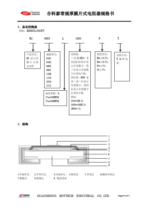
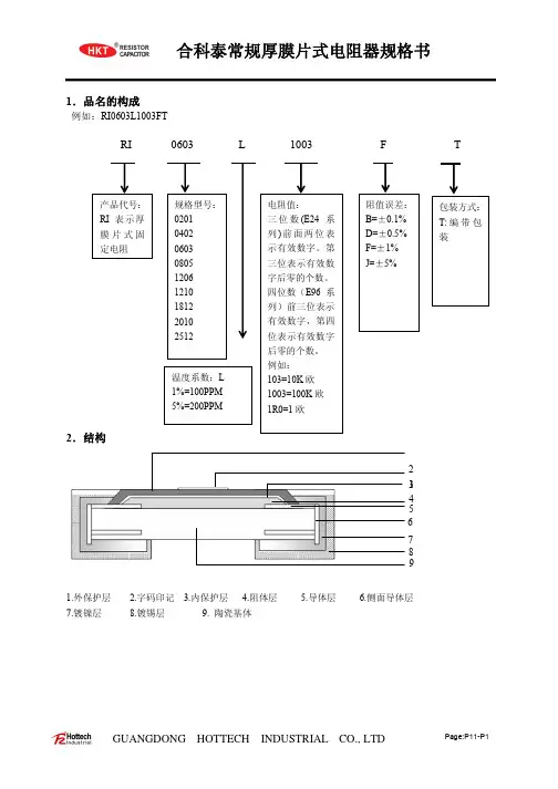
1.品名的构成例如:RI0603L1003FTRI 0603 L 1003 F T2.结构1.外保护层2.字码印记3.内保护层4.阻体层5.导体层6.侧面导体层7.镀镍层8.镀锡层9. 陶瓷基体2 3 4 5 6 7 8 913.尺寸和电性参数4.字码4.1 (大于1Ω表示方法)*0201、0402 因电阻本体太小,固无印记表示。
*公差为±0.1%、±0.5%、±1%的用四位数表示,前三位表示有效数字,第四位表示乘幂(10V)。
例如1003=100X103=100X1000=100000Ω=100KΩ4703=470X103.=470X1000=470000Ω=470KΩ22R1=22.1Ω(R表示小数点)1R30=1.3Ω(R表示小数点,不足四位在后面加0)*公差为±2%、±5%、用三位数表示,前二位数表示有效数字,第三位数表示乘幂(10V)。
例如103=10X103=10X1000=10000Ω=10KΩ473=47X103.=47X1000=47000Ω=47KΩ1R3=1.3Ω(R表示小数点)*E96代码表示, 公差为±0.1%、±0.5%、±1%用三位数表示(仅对0603表示)例如02C=102X102=102X100=10200Ω=10.2KΩ15E=140X104=140X10000=1400000Ω=1.4MΩ*公差为±0.1%、±0.5%、±1%(仅对0603表示)在E-24 系列中,但不属于E-96系列的阻值,标示和±5%的公差相同,但是在字码下多加一条横线.例如:124=120K4.2 (小于1Ω表示方法)*0201、0402 因电阻本体太小,固无印记表示。
*公差为±0.1%、±0.5%、±1%的用四位数表示,R表示小数点。
例如R200=0.2ΩR002=0.002Ω*公差为±2%、±5%、用三位数表示,R表示小数点。
Approval SheetforThick Film Chip ResistorRL series1% 2% 5%YAGEO CORPORATIONFactory: No.11, Min Chuan Rd., Ta Sheh, Kaohsiung, Taiwan, R.O.C.Tel: 886-7-351-4117 Fax: 886-7-352-6475Headquarters: 3F, No.233-1, Pao Chiao Rd., Hsin Tien, Taipei, Taiwan,R.O.C.Tel: 886-2-2917-7555 Fax: 886-2-2917-4286RL Series Version 2000-3 Page-1RL SeriesVersion 2000-3 Page-21. SUBJECT : This specification describes of RL series chip resistors made of YAGEOCorporation by thick film process.2. PART NUMBER : Part number of the chip resistor is identified by the series, size,tolerance, packing style, temperature coefficient, special type and resistance value.Example :RL 1206 F R - 07 0R02Series Size Resistance Packing Temperature Special ResistanceName Code Tolerance Style Coefficient Type Valueof Resistance(1) Size : (unit: inches)0603=0.063×0.033 1210=0.122×0.102 0805=0.083×0.051 2010=0.197×0.098 1206=0.122×0.0632512=0.250×0.126(2) Tolerance : F=±1%, G=±2%, J=±5%(3) Packaging Style : R =Paper Taping Reel. K =Embossed Plastic Tape Reel. C =Bulk Cassette.(4) T .C .R.: “-“Base on Spec.(5) Special Type : 07= 7 inch Dia. Reel10=10 inch Dia. Reel 13=13 inch Dia. Reel(6) Resistance Value : 10m Ω、20 m Ω、51 m Ω、100 m Ω、330 m Ω、470 m Ω……(7) Resistance Series : E24 (E48/96 on request)RL SeriesVersion 2000-3 Page-33. MARKING :(1) RL0805/RL1206/RL1210/RL2010/RL2512Either tolerance in 5% or 1%: 4 digits, uses MIL Standard resistance marking. “R” signifies decimal place.Value =20m Ω(2) RL0603Tolerance in 5%: 3 digits, uses MIL Standard resistance marking. “R” signifies decimal place.Value =220m Ω1% Tolerance : no marking4. POWER RATING(1) Rated Power at 70°C :RL0603=1/10WRL1210=1/3W RL0805=1/8W RL2012=3/4W RL1206=1/4WRL2512=1W(2) Rated Voltage : The DC or AC (rms) continuous working voltage correspondingto the rated power is determined by the following formula : V= √(P X R)Where V= Continuous rated DC or AC (rms) working voltage (V)P= Rated power (W) R= Resistance value (Ω)5. ELECTRICAL CHARACTERISTICSSTYLE RL0603 RL0805 RL1206 Operating Temp. Range -55°C ~ +125°CDerated to 0 Load at +125°CResistance Range 100mΩ≦Rn<1Ω 20mΩ≦Rn<1Ω 10mΩ≦Rn<1ΩTemperature Coefficient ±600ppm/°C±1500ppm/°CSTYLE RL1210 RL2010 RL2512 Operating Temp. Range -55°C ~ +125°CDerated to 0 Load at +125°CResistance Range 10mΩ≦Rn<1Ω 10mΩ≦Rn<1Ω 10mΩ≦Rn<1ΩTemperature Coefficient ±1500ppm/°CRL Series Version 2000-3 Page-4RL SeriesVersion 2000-3 Page-58. ENVIRONMENTAL CHARACTERISTICS(1) Temperature Coefficient of Resistance (T.C.R.)Test Method : Measure resistance at +25°C or specified room temperature asR 1, then measure at -55°C or +125°C respectively as R 2. Determine the temperature coefficient of resistance from the following formula.R 2-R 1 `T.C.R.= ----------------- X 106(PPM/°C) R 1 (t 2-t 1)Where t 1 =+25°C or specified room temperaturet 2 = -55°C or +125°C test temperatureR 1=resistance at reference temperature in ohms. R 2=resistance at test temperature in ohms.Acceptance Standard : (Refer to item 5)(2) Thermal ShockTest Method : -55±3°C, 2 minutes and +125±2°C, 2 minutes as one cycle. After5 cycles, the specimen shall be stabilized at room temperature for 1 hour minimum and then measure the resistance to determine △R/R(%).Acceptance Standard : ±1.0%(3) Low Temperature OperationTest Method : Place the specimen in a test chamber maintained at -65 °C. After one hour stabilization at this temperature, full rated workingvoltage shall be applied 45 minutes. Have15 minutes after remove the voltage, the specimen shall be removed from the chamber and stabilized at room temperature for 24 hrs. Measure the resistance to determine △R/R(%).Acceptance Standard : ±1.0%No mechanical damage.+5+5 -0 +0+0-5+5+5-0RL SeriesVersion 2000-3 Page-6(4) Short Time OverloadTest Method : Apply 2.5 times of rated voltage but not exceeding the maximumoverload voltage for 5 seconds. Have the specimen stabilized at room temperature for 30 minutes minimum. Measure the resistance to determine △R/R(%).Acceptance Standard : ± 1.0% for 1% tolerance± 2.0% for 2~5% toleranceNo evidence of mechanical damage(5) Insulation ResistanceTest Method : Place the specimen in the jig and apply a rated continuesoverload voltage (R.C.O.V) for one minute as shown. Measure the insulation resistance.Type Voltage Type Voltage RL0603 100V RL1210 400V RL0805 300V RL2010 400V RL1206 400V RL2512 400VAcceptance Standard : ≧10000M Ω(6) Dielectric Withstand VoltageTest Method : Place the specimen in the jig and apply a specified valuecontinuous overload voltage as shown for one minute.Type Voltage TypeVoltage RL0603 100V RL1210 400V RL0805 300V RL2010 400V RL1206 400V RL2512 400VAcceptance Standard : Breakdown voltage>specification and without open/short(7) Resistance to Soldering HeatTest Method: Immerse the specimen in the solder pot at 260±5°C for 10±1seconds. Have the specimen stabilized at room temperature for30 minutes minimum.Measure the resistance to determine △R/R(%).Acceptance Standard:±1.0% & no visible damage(8) Moisture ResistanceTest Method: Place the specimen in the test chamber, and subjected to 42damp heat cycles. Each one of which consists of the steps 1 to 7as figure 1. The total length of test is 1000 hours. After the test,have the specimen stabilized at room temperature for 24 hoursand measure the resistance to determine △R/R(%).Acceptance Standard:±2.0% & no visible damageFig.1 Conditions of change of temperatureRL Series Version 2000-3 Page-7RL SeriesVersion 2000-3 Page-8(9) LifeTest Method : Place the specimen in the oven at 70±2°C. Apply the rated voltageto the specimen at the 1.5 hours on and 0.5 hour off cycle. The total length of test is 1000 hours. After the test, have the specimen stabilized at room temperature for one hour minimum and measure the △R/R(%).Acceptance Standard : ± 2.0% for 1% tolerance± 3.0% for 2~5% tolerance(10) SolderabilityTest Method : Immerse the specimen in the solder pot at 230±5°C for 5 sec.Acceptance Standard : At least 95% solder coverage on the termination.9. TAPING REELUnit :mmStyle Packaging Tape width ∅A ∅B ∅C W TRL0603 RL0805 RL1206 RL1210Paper 8mm 180+0-360+1-0 13.0±0.29.0±0.3 11.4±1RL2010 RL2512Embossed 12mm 180+0-360+1-0 13.0±0.213.0±0.3 15.4±1RL SeriesVersion 2000-3 Page-910. PAPER TAPINGUnit : mmDimensionA B W E F P0 P1 P2 ΦD0 TRL0603 1.10±0.1 1.90±0.1 0.70±0.10RL0805 1.65±0.1 2.40±0.1 0.85±0.10RL1206 1.90±0.1 3.50±0.1 0.85±0.10RL12102.80±0.13.50±0.18.0±0.2 1.75±0.13.5±0.054.0±0.14.0±0.052.0±0.051.5+0.1 -00.85±0.1011. EMBOSSED TAPINGDimensionA B W E F P0P1P2ΦD0ΦD1TRL2010 2.8±0.2 5.4±0.2RL2512 3.5±0.2 6.7±0.212.0±0.3 1.75±0.15.5±0.054.0±0.14.0±0.12.0±0.05 1.5±0.1 1.5±0.25 1.0±0.112. PACKING METHODSPAPERRL Series Version 2000-3 Page-10。
MF06P, MF08P, MF12P, MF10P, MF20P, MF25P±1%, ±5% 1Ω~1MΩThick film High Power Chip ResistorsSize 0603, 0805, 1206, 1210, 2010, 2512 Automotive Grade & Anti-sulfur*Contents in this sheet are subject to change without prior notice.FEATURE1. Automotive grade AEC Q-200 compliant2. High reliability 1% stability3. 100% CCD inspection4. RoHS compliant and Halogen free and Lead free products5. High power rating up to 2W6. Anti-sulfur against H2S 3ppm 40’C, 90% RH, 1000hrsAPPLICATION1. High accuracy dc-power supply2. Digital multi-meter3. Telecommunication4. Computer5. Automotive industry6. Medical and military equipmentDESCRIPTIONThe resistors are constructed in a high grade ceramic body (aluminum oxide). Internal metal electrodes are added at each end and connected by a resistive paste that is applied to the top surface of the substrate. The composition of the paste is adjusted to give the approximate resistance required and the value is trimmed to nominated value within tolerance which controlled by laser trimming of this resistive layer.The resistive layer is covered with a protective coat. Finally, the two external end terminations are added. For ease of soldering the outer layer of these end terminations is a Tin (lead free) alloy.Fig 1. Construction of Chip-RQUICK REFERENCE DATA MF06PMF08PMF12PMF10PMF20PMF25PMF06PMF08PMF12PMF10PMF20PMF25PDIMENSIONS (unit: mm)MF06PMF08PMF12PMF10PMF20PM F25PMARKING3-digits marking(±1% : 0603)4-digits marking(±1% : 2512/ 2010/ 1210/ 1206/ 0805)Each resistor is marked with a four digits code on the protective coating to designate the nominal resistance value. ExampleFUNCTIONAL DESCRIPTIONProduct characterizationStandard values of nominal resistance are taken from the E96&E24 series for resistors with a tolerance of ±1%,±5%. The values of the E96/E24 series are in accordance with “IEC publication 60063”.DeratingThe power that the resistor can dissipate depends on the operating temperature; see Fig.2MOUNTINGDue to their rectangular shapes and small tolerances, Surface Mountable Resistors are suitable for handling by automatic placement systems.Chip placement can be on ceramic substrates and printed-circuit boards (PCBs).Electrical connection to the circuit is by individual soldering condition.The end terminations guarantee a reliable contact.SOLDERING CONDITIONThe robust construction of chip resistors allowsthem to be completely immersed in a solder bathof 260︒C for 10 seconds. Therefore, it is possibleto mount Surface Mount Resistors on one side ofa PCB and other discrete components on thereverse (mixed PCBs).Surface Mount Resistors are tested forsolderability at 235︒C during 2 seconds. The testcondition for no leaching is 260︒C for 30 seconds.Typical examples of soldering processes thatprovide reliable joints without any damage aregiven in Fig 3.Fig 3. Infrared soldering profile for Chip ResistorsCATALOGUE NUMBERSThe resistors have a catalogue number starting with:⏹Reeled tape packaging : 8mm width paper taping 5000pcs per 7” reel for 0603-1210 sizes.⏹Reeled tape packaging : 12mm width plastic taping 4000pcs per 7” reel for 2010, 2512 sizes.TEST AND REQUIREMENTS ( refer to AEC Q200 )PACKAGINGPaper Tape specifications(unit :mm)Reel dimensions。
ContentsIntroduction ………………………………………………………………………………………Page1.0 Scope (4)2.0 Ratings & Dimension ………………………………………………………….…………....4~53.0 Structure (5)4.0 Marking…….……………………………………… ………………………..… …………..…6~75.0 Derating Curve................................................ .. (8)6.0 Performance Specification …………………………………………………………..............8~97.0 Explanation of Part No. System (10)8.0 Ordering Procedure (11)9.0 Packing ………………….…………………………………………………………………..…11~1310.0 Note Matter (14)File Name:CHIP SERIES±0.5%,±1%,±2%,±5%& 0ΩDate 2015.02.04EditionNo. 1Amendment Record Signature Edition Prescription of amendment Amend Page Amend Date Amended by Checked byThis specification for approve relates to the Lead-Free Thick Film Chip Resistors manufactured byROYALOHM.2.0 Ratings & Dimension:01005、0201、04020603、0805、1206、1210、1812、2010、25122.1 Dimension & Resistance Range :Type70℃ PowerDimension(mm) Resistance RangeL W H A B 0.5% 1.0% 2.0% 5.0%01005 1/32W 0.40±0.02 0.20±0.02 0.13±0.02 0.10±0.050.10±0.03-- 10Ω-10M Ω 10Ω-10M Ω10Ω-10M Ω0201 1/20W 0.60±0.03 0.30±0.03 0.23±0.03 0.10±0.050.15±0.05-- 1Ω-10M Ω 1Ω-10M Ω1Ω-10M Ω0402 1/16W 1.00±0.100.50±0.05 0.35±0.05 0.20±0.100.25±0.101Ω-10M Ω0.1Ω~22M Ω 0.1Ω~22M Ω0.1Ω~22M Ω06031/16W 1/10WS1.60±0.10 +0.150.80-0.100.45±0.10 0.30±0.200.30±0.201Ω-10M Ω0.1Ω~33M Ω 0.1Ω~33M Ω0.1Ω~100M Ω08051/10W 1/8WS2.00±0.15 +0.151.25-0.10 0.55±0.10 0.40±0.200.40±0.201Ω-10M Ω0.1Ω~33M Ω 0.1Ω~33M Ω0.1Ω~100M Ω12061/8W 1/4WS 3.10±0.15+0.15 1.55 -0.100.55±0.10 0.45±0.200.45±0.201Ω-10M Ω0.1Ω~33M Ω 0.1Ω~33M Ω0.1Ω~100M Ω1210 1/4W1/3WS 1/2WSS 3.10±0.10 2.60±0.20 0.55±0.10 0.50±0.250.50±0.201Ω-10M Ω0.1Ω~10M Ω 0.1Ω~22M Ω0.1Ω~100M Ω1812 1/2W 3/4WS4.50±0.20 3.20±0.20 0.55±0.20 0.50±0.200.50±0.201Ω-10M Ω0.1Ω-10M Ω 0.1Ω-10M Ω0.1Ω-10M Ω20101/2W 3/4WS5.00±0.10 2.50±0.20 0.55±0.10 0.60±0.250.50±0.201Ω-10M Ω0.1Ω~22M Ω 0.1Ω~22M Ω0.1Ω~22M Ω2512 1W 6.35±0.10 3.20±0.20 0.55±0.10 0.60±0.250.50±0.201Ω-10M Ω0.1Ω~33M Ω 0.1Ω~33M Ω0.1Ω~33M ΩType70℃PowerMax 。
FEATURESZINC OXIDE VARISTORAre non-linear resistors utilize a semiconductor electronic ceramic element mainly composed of Zinc Oxide and its resistors change as a function of the applied voltage .It s called Varistor or Transient surge absorbers(18V~1.8KV)(25ns)(2000A/cm 2)Widely voltage range 18V~1.8KVFast response to the rapidly increase Voltage(25ns)Excellent non-linearity voltage Symmetric V-l characteristicsGreat withstanding surge current (2000A/cm )No follow-on current Long life2HOW TOORDERCHARACTERISTICSpre breakdownregionnomal operatingregion upturn regionFig1Voltage Current CharacteristicCurrent(A)V O L T A G E (V )1031021010-810-710-610-510-410-310-210-111010*********5LEAD STYLEF Inside Crimped shortQUANTITY&MEASUREFig.AFig.BFig.CFig.DFig.EFig.FZINC OXIDE VARISTORT Thickness (max)(Unit:mm)DIMENSION40K48521811.50.05TAPING SPECIFICATIONUnit:mm1.0ZINC OXIDE VARISTORK5SERIES SPECIFIATION5SeriesK7060410756983020155040200901008015030040060050030906040508070200150100400300800900700Current(A)Current(A)V-I CurveImpluse Lifetime Ratings(2time:5minutes internalup to 10times 2minutes internal up to 10times 10seconds internal)6V o l t a g e (V )Impulse width u s)Impulse width u s)ZINC OXIDE VARISTOR7K SERIES SPECIFIATION FNR-07K681420561680(612~748)7KSeriesImpulse width u s)V-I CurveCurrent(A)Impluse Lifetime Ratings(2time:5minutes internalZINC OXIDE VARISTORFNR-10K11210K SERIES SPECIFIATION6808951100(990~1210)10KSeriesImpluse Lifetime RatingsV-I Curvet ((I m p u l s e w i d t h (s )V o l t a g e (V )ZINC OXIDE VARISTORFNR-14K18214K SERIES SPECIFIATION100014651800(1620~1980)ZINC OXIDE VARISTOR14K Series)V(egatloVI m p u l s e w i d t h(s)FNR-20K18220K SERIES SPECIFIATION100014651800(1620~1980)20KSeriesImpluse Lifetime RatingsV-I CurveI m p u l s e w i d t h (s )V o l t a g e (V )C u r r e n t ()ZINC OXIDE VARISTOR25K SERIES SPECIFIATION FNR-25K182100014651800(1620~1980)25KSeriesV-I CurveV o l t a g e (V )I m p u l s e w i d t h (s )ZINC OXIDE VARISTORFNR-32K1821000146532K SERIES SPECIFIATION1800(1620~1980)32KSeriesV-I CurveV o l t a g e (V )C u r r e n t ()I m p u l s e w i d t h (s )V o l t a g e (V )C u r r e n t ()I m p u l s e w i d t h (s )ZINC OXIDE VARISTOR40K SERIES SPECIFIATION FNR-40K182100014651800(1620~1980)40KSeriesV-I CurveV o l t a g e (V)C u r r e n t ()I m p u l s e w i d t h (s )V o l t a g e (V )ZINC OXIDE VARISTOR()HOW TO SELECT A VARISTOR(ONL Y REFERENCE)A:V=a v/b c1mAa 1.2vb0.85c0.9A:Varistor voltageVaristor Voltage should be more than the operating voltage in over protective circuit,The formula is shown as the following.V=a v/b c1mAa-power Voltage ripple coefficient usually1.2v-DC Voltage(significant value only AC power)b-Tolerance usually take0.85c-Ageing coefficient usually take0.9B:50%B:Withstanding surge currentIn general,withstanding surge current is max,Pulse current value which determined by test conditions such as wave-shape,amplitude and intermal time,when the amplitude decrease to50%of the initial, it should be increased to2times of the initial in order to keep the life longer,the surge current which is sbsorbed by the varistor should be less than max.withstanding surge currentZINC OXIDE VARISTOR APPLICATIONSFNR-05K391FNR-07K391FNR10K391(SELECT OF FUSE in conformity to FNR Varistor) If conform with diameter):If conform with Max Peak current):Fuse ratingZINC OXIDE VARISTORELECTRICAL PERFORMANCE TEST:5~35:45%~85%Standardl Test Conditions:Tempreture:5~35,humidity:45%~85%(Machinecharacteristic test)ZINC OXIDE VARISTOR。
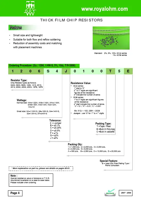
RoHS CompliantType02010402060308051206121020102512Max. Working Voltage 25V 50V 50V 150V 200V 200V 200V 200VMax. Overload Voltage50V 100V 100V 300V 400V 400V 400V 400V Dielectric withstanding Voltage -100V300V500V500V500V500V500VOperating Temperature-55~+155°C -55~+155°C -55~+155°C -55~+155°C -55~+155°C -55~+155°C -55~+155°C -55~+155°CType02010402060308051206121020102512Power Rating at 70°C1/20W 1/16W 1/16W (1/10W-S)1/10W (1/8W-S)1/8W (1/4W-S)1/4W (1/3W-S) *1/2W (3/4W-S)1W L (mm)0.60 ± 0.03 1.00 ± 0.10 1.60 ± 0.10 2.00 ± 0.15 3.10 ± 0.15 3.10 ± 0.10 5.00 ± 0.10 6.35 ± 0.10W (mm)0.30 ± 0.030.50 ± 0.050.80+0.15 -0.101.25+0.15 -0.101.55+0.15 -0.102.60+0.15 -0.102.50+0.15 -0.103.20+0.15 -0.10DimensionH (mm)0.23 ± 0.030.35 ± 0.050.45 ± 0.100.55 ± 0.100.55 ± 0.100.55 ± 0.100.55 ± 0.100.55 ± 0.10A (mm)0.10 ± 0.050.20 ± 0.100.30 ± 0.200.40 ± 0.200.45 ± 0.200.50 ± 0.250.60 ± 0.250.60 ± 0.25B (mm)0.15 ± 0.050.25 ± 0.100.30 ± 0.200.40 ± 0.200.45 ± 0.200.50 ± 0.200.50 ± 0.200.50 ± 0.20Resistance Value of Jumper <50mΩ<50mΩ<50mΩ<50mΩ<50mΩ<50mΩ<50mΩ<50mΩRated Current of Jumper 0.5A 1A 1A 2A 2A 2A 2A 2A Max. Current of Jumper 1A 2A 2A 5A 10A 10A 10A 10A Resistance Range of 0.5% (E-96)10Ω ~ 1MΩ1Ω ~ 10MΩ1Ω ~ 10MΩ1Ω ~ 10MΩ1Ω ~ 10MΩ1Ω ~ 10MΩ1Ω ~ 10MΩ1Ω ~ 10MΩResistance Range of 1% (E-96)10Ω ~ 1MΩ1Ω ~ 10MΩ1Ω ~ 10MΩ1Ω ~ 10MΩ1Ω ~ 10MΩ1Ω ~ 10MΩ1Ω ~ 10MΩ1Ω ~ 10MΩResistance Range of 2% (E-24)10Ω ~ 1MΩ1Ω ~ 10MΩ1Ω ~ 10MΩ1Ω ~ 10MΩ1Ω ~ 10MΩ1Ω ~ 10MΩ1Ω ~ 10MΩ1Ω ~ 10MΩResistance Range of 5% (E-24)1Ω ~ 1MΩ1Ω ~ 10MΩ1Ω ~ 10MΩ1Ω ~ 10MΩ1Ω ~ 10MΩ1Ω ~ 10MΩ1Ω ~ 10MΩ1Ω ~ 10MΩ* 1210 size in 1/2W could be provided specially (1210U2)• Small size & light weight• Reduction of assembly costs and matching with placement machine • Suitable for both flow & re-flow soldering• Applications: Navigator (GPS), Mobile Phone,Telecom, PDA, Setbox, Meter.FeatureFiguresDerating Curve & SpecificationThick Film Chip ResistorsP e r c e n t r a t e d l o a d (%)Ambient termperature(°C )2UniOhmRoHS CompliantValue Code Value Code Value Code Value Code Value Code Value Code100011471721533316494646568181102021501822134324504756669882105031541922635332514876771583107041582023236340524996873284110051622123737348535116975085113061652224338357545237076886115071692324939365555367178787118081742425540374565497280688121091782526141383575627382589124101822626742392585767484590127111872727443402595907586691130121912828044412606047688792133131962928745422616197790993137142003029446432626347893194140152053130147442636497995395143162103230948453646658097696Thick Film Chip Resistors• For 0201 & 0402 size, no marking on the body due to the small size of the resistor.• ±5% tolerance product: the marking is 3 digits, the first 2 digits are the significant of the resistance and the 3rd digit denotes number of zeros following.• 0805, 1206, 1210, 2010, 2512 ±1%: the marking is 4 digits, the first 3 digits are the signivicant of the resistance and the 4th digit denotes number of zeros following.Marking on the Resistors Body2372 = 23700Ω = 23.7KΩ; 1430 = 143ΩBelow 10Ω : 3R24 = 3.24Ω153 = 15000Ω = 15KΩ; 120 = 12ΩBelow 10Ω: 6R8 = 6.8Ω• Standard E-96 series values of 0603 ±1%: due to the small size of the resistor’s body, 3 digits marking will be used to indicate the accurate resistance value by using the following Multiplier & Resistance Code.Multiplier Code (for 0603 1% marking)So the resistance value are marked as the following examples:1.96KΩ= 196 ×101 Ω = 29B12.4Ω= 124 ×10 -1 = 10X• Standard E-24 and not belong to E-96 series values (±1%) of 0603 size: the marking is te same as 5% tolerance but marking as underline.122 = 1200 = 1.2 KΩ680 = 68ΩStandard E-96 Series Resistance Value Code (for 0603 1% marking)Code A B C D E F G H X Y Z Multiplier10010110210310410510610710-110-210-3UniOhm3RoHS CompliantTemperature coefficiant1Ω~10Ω ≤ ±400PPM/°C11Ω~100Ω ≤ ±200PPM/°C>100Ω ±100PPM/°C (0201: >100Ω ±200PPM/°C ) Short-time overload±5%, ± 2%: ±(2.0% + 0.1Ω) Max.±1%, ± 0.5%: ±(1.0% + 0.1Ω) Max. Insulation resistance≥ 1,000 Mega OhmDielectronic withstanding voltageNo evidence of flashover, mechanical damage, arcing or insulation breakdown Terminal bending ±(1.0% + 0.05Ω) Max. Solering heat ±(1.0% + 0.05Ω) Max. Solerability Min. 95% coverageTemperature cycling±5%, ± 2%: ±(1.0% + 0.05Ω) Max.±1%, ± 0.5%: ±(0.5% + 0.05Ω) Max. Humidity (Steady State)±5%, ± 2%: ±(3.0% + 0.1Ω) Max.±1%, ± 0.5%: ±(0.5% + 0.1Ω) Max. Load life in humidity±5%, ± 2%: ±(3.0% + 0.1Ω) Max.±1%, ± 0.5%: ±(1.0% + 0.1Ω) Max. Load life±5%, ± 2%: ±(3.0% + 0.1Ω) Max.±1%, ± 0.5%: ±(1.0% + 0.1Ω) Max.• The values which are not of standard E-24 series (2% & 5%) and not of E-96 series (1%) could be offered on a case to case basis.Special Feature:E = Lead Free (standard)Resistance Value : 5% (E-24 series):the 1st digit is “0”, the 2nd & 3rd digits are for the significant figures of the resistance and the 4th indicate the numbers of zeros following; 1% (E-96 series):the 1st to 3rd digits are for the signifi-cant figures of the resistance and the 4th indicate the numbers of zeros following.Tolerance:F = ±1%G = ±2%J = ±5%R =0~30%: Q =0~20%:N =-20~0%P =-30~0%:K =±10%:M =±20%:Wattage:Fill-in 2 digits with the codes as fol-low:WH=1/32W WM=1/20W , WG=1/16W , WA=1/10W , 1W=1W , W2=1/2W W4=1/4W , W8=1/8W , SA=1/10W-S, S8=1/8W-S, S4=1/4W-S, S3=1/3W-S, U2=1/2W-SS 07=3/4W-SProduct Type:Fill-in 4 digits with the Chip resistor type as follow:0201, 0402, 0603, 0805, 1206, 1210, 2010, 2512, 2D02, 2C02, 4D02, 4C02, 4D03, 4C03, 16P8, 10P8, 10S8, 10T8, 10E9, TR05, TR06, HP03, HP05, HP06, CS12, 1218, 0612, 1020.Ordering Procedure (Example: 1206 1/4W-S 5% 1.2 Ω T/R-5000)Performance SpecificationsThick Film Chip Resistors4UniOhm。
厚生金属电阻厚生金属电阻是一种常见的电子元件,它在电路中起着限制电流、稳定电压和改变电阻值的作用。
作为一种重要的电阻器,厚生金属电阻在各个领域都有广泛的应用。
厚生金属电阻的特点之一是其材料的选择。
它通常由金属铜、镍、铬等材料制成,这些材料具有良好的导电性和稳定性,能够在不同的工作环境下保持稳定的电阻值。
此外,厚生金属电阻还具有较高的功率耗散能力,能够承受较大的电流,不易受到过载或过热的影响。
厚生金属电阻的工作原理是基于电阻效应。
当电流通过厚生金属电阻时,金属材料内的电子会受到电阻的阻碍,导致电子的运动速度减慢,进而产生电阻。
根据欧姆定律,电阻值与电流成正比,与电压成反比。
因此,可以通过改变电流或电压来改变厚生金属电阻的阻值。
厚生金属电阻常用于电子电路中的限流电阻。
在电路中,为了保护其他元件免受过大的电流损害,需要加入适当大小的限流电阻。
厚生金属电阻由于其稳定性和功率耗散能力较强的特点,常被用作限流电阻。
通过选择合适的电阻值,可以实现对电路中电流的精确控制。
厚生金属电阻还常用于稳压电路中。
在一些需要稳定电压输出的场合,如电源、稳压器等,需要通过电阻来实现电压的稳定。
厚生金属电阻由于其稳定的电阻值和耐高温的特点,能够在这些场合中起到很好的稳压作用。
通过在电路中串联厚生金属电阻,可以有效地限制电压的变化范围,从而保证输出电压的稳定性。
厚生金属电阻还可以用于测量电流和电压。
在电路测试和仪器仪表中,常需要对电流和电压进行测量。
厚生金属电阻可以作为电流表和电压表的内部电阻,通过测量其上的电压降或电流值,来间接测量电路中的电流和电压。
由于厚生金属电阻的稳定性和精确性较高,能够提供较为准确的测量结果。
厚生金属电阻作为一种重要的电子元件,具有广泛的应用领域。
它可以用于限流、稳压、测量等方面,起到稳定电流、稳定电压和改变电阻值的作用。
在设计电子电路或选择电阻元件时,我们可以根据具体的需求和要求,选用合适的厚生金属电阻,以实现电路的稳定运行和精确控制。
直热式负温度系数热敏电阻器规格书Directly heated negative temperature coefficient thermistorsNTC Specification客户名称 CUSTOMER NAME产品名称 PART NAME MF72 NTC热敏电阻产品规格 PART NUMBER NTC5D-7签发日期 ISSUE DATE2023-12-05确认CONFIRM产品规格代码和应用范围及特点PartNumber and Application Range and Characteristics一、产品规格代码 PARTNUMBER二、应用范围及特点Application Range and Characteristics1、产品特点 FeatureofPowerThermistor1.1应用范围 Appliaction1.2特点 Characteristic○转换电源,开关电源,UPS电源○Switchingpower-supply,switchpower,upspower ○镇流器及各类加热器 ○Electronicenergysavinglampselectronicballast and all kindsofelectricheater ○各类显像管,显示器 ○AllkindsofRT,display ○电子节能灯,其他照明灯具○Bulbandotherlightinglamps○体积小,功率大,抑制浪涌电流能力强○Smallsize,largepower,strongcapacityof suppressionofinrushcurrent ○反应速度快○Fastresporse○材料常数(B值)大,残余电阻小○Bigmaterialconstant(Bvalue),small residualresistance ○寿命长,可靠性高○Longlifeandhighreliability ○系列全,应用范围宽○Completeseries,wideapplications外型尺寸及材料和电性能External dimensions and material and electrical properties一、外型尺寸及相关标准External dimensions and relevant standards3 产品尺寸 Product size4 材料 Materials(1)封装材料(Wrapper) :酚醛树脂(Modified phenolic resin)(2)引线(Down-lead) :CP线(CP Wire)(3)颜色(Coating color):黑色(Black)二、电性能Electrical performance1 引线形状 Lead the shape2 产品标识 Product identificationNTC 5D-7NTC负温度系数热敏电阻器 NTCthermistor 5额定零功率电阻值 5ΩD 圆片型Disk-Type7直径 7±1(mm)型号Part NoD maxT maxd ±0.05F ±1P max直引线StraightLead WireL15D-7950.555420型号R25(Ω)最大稳态电流(A)残余电阻(Ω)耗散系数(mw/℃)热时间常数(s)最大允许使用容量值240V/120V(μF)B值(K)工作温度(℃)认证UL/CULCQCTUV5D-7520.28约9约30100/3902700-40~ +150pass pass pass产品结构、材料及制造工艺流程Product structure, materials and manufacturing process flow 一、NTC 热敏电阻产品结构 NTC Thermisto Product structure二、材料 Materials三、制造工艺流程 Manufacturing process flowMF72型NTC热敏电阻工艺流程图备注:所有工序工人必须自检.产品阻温特性及静态伏安特性Resistance-Temperature Characteristic and Staracteristic 一、产品阻温特性Resistance-Temperature Characteristic二、静态伏安特性Staracteristic热敏电阻技术术语及安全可靠性properties of products一、HEL热敏电阻技术术语二、电气性能 Electrical Characteristics三、机械性能Mechanical Characteristics四、可靠性试验Reliability TestSafety regulation certification and corresponding modelPacking methods 一、散装式样 BULK STYLE(1)常规产品包装Normal product packaging(2)切脚产品包装 Cut the feet product packaging二、编带包装式样Packing style编带尺寸Tape size存储条件Storage condition1 存贮环境条件2 请不要在下列条件下使用本元件,否则将可能导致性能衰退或产品损毁,甚至引起火灾。
ContentsIntroduction ………………………………………………………………………………………Page1.0 Scope (4)2.0 Ratings & Dimension ………………………………………………………….…………....4~53.0 Structure (5)4.0 Marking…….……………………………………… ………………………..… …………..…6~75.0 Derating Curve................................................ .. (8)6.0 Performance Specification …………………………………………………………..............8~97.0 Explanation of Part No. System (10)8.0 Ordering Procedure (11)9.0 Packing ………………….…………………………………………………………………..…11~1310.0 Note Matter (14)File Name:CHIP SERIES±0.5%,±1%,±2%,±5%& 0ΩDate 2015.02.04EditionNo. 1Amendment Record Signature Edition Prescription of amendment Amend Page Amend Date Amended by Checked byThis specification for approve relates to the Lead-Free Thick Film Chip Resistors manufactured byROYALOHM.2.0 Ratings & Dimension:01005、0201、04020603、0805、1206、1210、1812、2010、25122.1 Dimension & Resistance Range :Type70℃ PowerDimension(mm) Resistance RangeL W H A B 0.5% 1.0% 2.0% 5.0%01005 1/32W 0.40±0.02 0.20±0.02 0.13±0.02 0.10±0.050.10±0.03-- 10Ω-10M Ω 10Ω-10M Ω10Ω-10M Ω0201 1/20W 0.60±0.03 0.30±0.03 0.23±0.03 0.10±0.050.15±0.05-- 1Ω-10M Ω 1Ω-10M Ω1Ω-10M Ω0402 1/16W 1.00±0.100.50±0.05 0.35±0.05 0.20±0.100.25±0.101Ω-10M Ω0.1Ω~22M Ω 0.1Ω~22M Ω0.1Ω~22M Ω06031/16W 1/10WS1.60±0.10 +0.150.80-0.100.45±0.10 0.30±0.200.30±0.201Ω-10M Ω0.1Ω~33M Ω 0.1Ω~33M Ω0.1Ω~100M Ω08051/10W 1/8WS2.00±0.15 +0.151.25-0.10 0.55±0.10 0.40±0.200.40±0.201Ω-10M Ω0.1Ω~33M Ω 0.1Ω~33M Ω0.1Ω~100M Ω12061/8W 1/4WS 3.10±0.15+0.15 1.55 -0.100.55±0.10 0.45±0.200.45±0.201Ω-10M Ω0.1Ω~33M Ω 0.1Ω~33M Ω0.1Ω~100M Ω1210 1/4W1/3WS 1/2WSS 3.10±0.10 2.60±0.20 0.55±0.10 0.50±0.250.50±0.201Ω-10M Ω0.1Ω~10M Ω 0.1Ω~22M Ω0.1Ω~100M Ω1812 1/2W 3/4WS4.50±0.20 3.20±0.20 0.55±0.20 0.50±0.200.50±0.201Ω-10M Ω0.1Ω-10M Ω 0.1Ω-10M Ω0.1Ω-10M Ω20101/2W 3/4WS5.00±0.10 2.50±0.20 0.55±0.10 0.60±0.250.50±0.201Ω-10M Ω0.1Ω~22M Ω 0.1Ω~22M Ω0.1Ω~22M Ω2512 1W 6.35±0.10 3.20±0.20 0.55±0.10 0.60±0.250.50±0.201Ω-10M Ω0.1Ω~33M Ω 0.1Ω~33M Ω0.1Ω~33M ΩType70℃PowerMax 。
Working VoltageMax 。
Overload VoltageDielectric withstanding VoltageResistance Value of JumperRated Current of JumperMax 。
Rated Current of JumperOperating Temperature01005 1/32W 15V 30V -- <50m Ω -- -- -55℃~155℃0201 1/20W 25V 50V -- <50m Ω 0.5A 1A -55℃~155℃0402 1/16W 50V 100V100V <50m Ω 1A 2A -55℃~155℃06031/16W 1/10WS 75V 150V 300V <50m Ω 1A 2A -55℃~155℃0805 1/10W 1/8WS 150V 300V 500V <50m Ω 2A 5A -55℃~155℃1206 1/8W 1/4WS 200V 400V 500V <50m Ω 2A 10A -55℃~155℃1210 1/4W1/3WS 1/2WSS200V 500V 500V <50m Ω 2A 10A -55℃~155℃18121/2W 3/4WS 200V 500V 500V <50m Ω 2A 10A -55℃~155℃2010 1/2W 3/4WS200V 500V 500V <50m Ω 2A 10A -55℃~155℃2512 1W 200V 500V 500V <50m Ω 2.5A 10A -55℃~155℃3.0 Structure:4.0 Marking:(1) For 01005、0201 and 0402 size. Due to the very small size of the resistor’s body, there is no marking on thebody.Example:01005、0201、0402(2) ±2%,±5%Tolerance:The first two digits are significant figures of resistance and the third denotes number ofzeros followingExample:33000 → 33KΩ(3) ±2%、±5%Tolerance: Below 10Ω show as following, read alphabet”R” as decimal point.Example:2R2 → 2.2Ω(4) ±0.5%、±1% Tolerance: 4 digits, first three digits are significant; forth digit is number of zeros. Letter r is decimalpoint.2701 → 2.7KΩ10R0 → 10Ω(5) standard E-24 and not belong to E-96 series values(in ±0.5%、±1%tolerance)of 0603 size the marking is thesame as 5% tolerance but marking as underline333=33000→33KΩ680→68Ω(6) Standard E-96 series values (±0.5%、±1% tolerance) of 0603 size. Due the small size of the resistor’s body, 3digits marking will be used to indicate the accurate resistance value by using the following multiplier &resistance code.Multiplier code:Code A B C D E F G H X Y Z Multiplier100 101 102 103 104 105 106 107 10-1 10-2 10-3 Coding formulaFirst two digits------------Resistance code Third digit-------------------Multiplier codeEXAMPLE: 1.96KΩ=196×101Ω------29B 12.4Ω=124×10-1Ω-----10XSTANDARD E-96 VALUES AND 0603 RESISTANCE CODEΩ VALUE CODE Ω VALUE CODE Ω VALUE CODE Ω VALUE CODE 100 01 178 25 316 49 562 73 102 02 182 26 324 50 576 74 105 03 187 27 332 51 590 75 107 04 191 28 340 52 604 76 110 05 196 29 348 53 619 77 113 06 200 30 357 54 634 78 115 07 205 31 365 55 649 79 118 08 210 32 374 56 665 80 121 09 215 33 383 57 681 81 124 10 221 34 392 58 698 82 127 11 226 35 402 59 715 83 130 12 232 36 412 60 732 84 133 13 237 37 422 61 750 85 137 14 243 38 432 62 768 86 140 15 249 39 442 63 787 87 143 16 255 40 453 64 806 88 147 17 261 41 464 65 825 89 150 18 267 42 475 66 845 90 154 19 274 43 487 67 866 91 158 20 280 44 499 68 887 92 162 21 287 45 511 69 909 93 165 22 294 46 523 70 931 94 169 23 301 47 536 71 953 95 174 24 309 48 549 72 976 96(7) 0ΩMarking:Normally for 01005、0201 and 0402 size, no marking on the body:Normally, the making of 0Ω 0603, 0Ω 0805, 0Ω 1206, 0Ω 1210, 0Ω 1812, 0Ω 2010, 0Ω 2512 resistors asfollowing5.0 Derating Curve:Resistors shall have a power rating based on continuous load operation at an ambient temperature from -55℃ to 70℃. For temperature in excess of 70℃, the load shall be derate as shown in figure 1Figure 15.1 Voltage rating:Resistors shall have a rated direct-current (DC) continuous workingVoltage or an approximate sine-wave root-mean-square (RMS) alternating-current (AC) continuous working voltage at commercial-line frequency and waveform corresponding to the power rating, as determined from the following formula:RCWV =R P ×Where: RCWV commercial-line frequency and waveform (Volt.)P = power rating (WATT.) R = nominal resistance (OHM)In no case shall the rated DC or RMS AC continuous working voltage be greater than the applicablemaximum value.The overload voltage is 2.5 times RCWV or Max. Overload voltage whichever is less.◎ *Solderability 95% coverage Min.Wave solder:Test temperature of solder: 245℃±3℃ dipping time in solder: 2-3 seconds.Soldering temp referenceElectrical characteristics shall besatisfied. Without distinct deformation in appearance. (95 % coverage Min.)Wave soldering condition: (2 cycles Max.) Pre-heat: 100~120,30±℃ 5 sec.Suggestion solder temp.: 235~255,10℃sec. (Max.) Peak temp.: 260℃Reflow soldering condition: (2 cycles Max.) Pre-heat:150~180,90~120℃sec.Suggestion solder temp.: 235~255,20~40℃sec. Peak temp.: 260℃Hand soldering condition:The soldering iron tip temperature should be less than 300and maximum contract t ℃ime should be 5 sec.◎ Temperaturecycling±0.5%,±1%±(0.5%+0.05 Ω)4.19Resistance change after continuous five cycles for duty cycle specified below:Step Temperature Time 1 -55℃±3℃ 30 mins 2 Room temp. 10 --- 15 mins 3 +155℃±2℃ 30 mins 4 Room temp. 10 --- 15 mins±2%,±5% ±(1.0%+0.05 Ω)01005 ±(1%+0.05Ω)◎ Solderingheat Resistance change rate is:±(1.0%+0.05Ω)4.18 Dip the resistor into a solder bath having a temperatureof 260℃±5℃ and hold it for 10±1 seconds. Terminal bending ±(1.0%+0.05Ω) 4.33 Twist of test board:Y/x = 3/90 mm for 60Seconds* Insulation resistance 1,000 M Ω or more4.6 Apply 500V DC between protective coating and termination for 1 min, then measure.◎ Humidity ( steady state )±0.5%,±1%±(0.5%+0.1Ω) 4.24Temporary resistance change after 240 hours exposure in a humidity test chamber controlled at 40±2℃ and 90-95% relative humidity,±2%,±5% ±(3.0%+0.1Ω) 01005±(3.0%+0.05Ω) ◎ *Load life in humidity±0.5%,±1%±(1.0%+0.1Ω) 7.9 Resistance change after 1,000 hours (1.5 hours “ON”,0.5 hour “OFF”) at RCWV in a humidity chamber controlled at 40℃±2℃ and 90 to 95% relative humidity. ±2%,±5% ±(3.0%+0.1Ω) 01005±(3.0%+0.05Ω)* <50m ΩApply to rated current for 0Ω◎ *Load life±0.5%,±1% ±(1.0%+0.1Ω) 4.25.1 Permanent resistance change after 1,000 hoursoperating at RCWV with duty cycle 1.5 hours “ON”, 0.5 hour “OFF” at 70℃±2℃ ambient. ±2%,±5% ±(3.0%+0.1Ω) 01005 ±(3.0%+0.05Ω)* <50m ΩApply to rated current for 0ΩThe resistors of 0Ω only can do the characteristic noted of *The resistors of 01005 & 0201 only can do the characteristic noted of ◎7.0 Explanation of Part No. System:The standard Part No. includes 14 digits with the following explanation:7.1 1st ~4th digitsThis is to indicate the Chip Resistor.Example: 01005, 0201, 0402,0603,0805,1206,1210,2010,1812,25127.2 5th~6th digits:7.2.1 This is to indicate the wattage or power rating. To dieting the size and the numbers,The following codes are used; and please refer to the following chart for detail:W=Normal Size; S=Small Size; U= Ultra Small Size; “1"~“G"to denotes“1"~“16"as Hexadecimal:1/16W~1W:1/2 1/3 1/4 1/8 1/10 1/16 1/20W 13/4WWattage 1/32Size WH 07 W2 W3 W4 W8 WA WG WM 1W NormalSize / 07 S2 S3 S4 S8 SA SG / 1S Small7.2.2 For power rating less or equal to 1 watt, the 5th digit will be the letters W or S to represent the size required & the 6th digit will be a number or a letter code.Example: WA=1/10W; S4=1/4W-S7.3 The 7th digit is to denote the Resistance Tolerance. The following letter code is to be used for indicating the standard Resistance Tolerance.D=±0.5% F=±1% G=±2% J=±5% K= ±10%7.4 The 8th to 11th digits is to denote the Resistance Value.7.4.1 For the standard resistance values of 5%&10% series, the 8th digit is “0",the 9th & 10th digits are to denote the significant figures of the resistance and the 11th digit is the number of zeros following;For the standard resistance values of ≤2% series in, the 8th digit to the 10th digits is to denote the significant figures of the resistance and the 11th digit is the zeros following.7.4.2 The following number s and the letter codes are to be used to indicate the number of zeros in the 11th digit:0=100 1=101 2=102 3=103 4=104 5=105 6=106 J=10-1K=10-2 L=10-3 M=10-47.4.3 The 12th, 13th & 14th digits.The 12th digit is to denote the Packaging Type with the following codes:C=Bulk in (Chip Product) T=Tape/Reel7.4.4 The 13th digit is normally to indicate the Packing Quantity of Tape/Reel packaging types. The following letter code is to be used for some packing quantities:4=4000pcs 5=5000pcs C=10000pcs D=20000pcs E=15000pcs Chip Product: BD=B/B-20000pcs TC=T/R-10000pcs7.4.5 For some items, the 14th digit alone can use to denote special features of additional information with the following codes:E= For “Environmental Protection, Lead Free type".S= Provided Specially.8.0 Ordering Procedure: ( Example: 0805 1/8WS ±5% 10K Ω T/R-5000 )0 8 0 5 S 8 J 0 1 0 3 T 5 E9.0 Packaging:9.1 Tapping Dimension:Unit: mmTypeABC ±0.05+0.1 ΦD -0E ±0.1F ±0.05G ±0.1 W ±0.2 T ±0.101005 0.24±0.05 0.45±0.05 2.00 1.50 1.75 3.50 4.00 8.00 0.40 0201 0.40±0.05 0.70±0.05 2.00 1.50 1.75 3.50 4.00 8.00 0.42 0402 0.65±0.20 1.15±0.20 2.00 1.50 1.75 3.50 4.00 8.00 0.45Unit: mm Type A ±0.2 B ±0.2 C ±0.05 +0.1 ΦD-0 E ±0.1F ±0.05 G ±0.1 W ±0.2 T ±0.10603 1.10 1.90 2.00 1.50 1.75 3.50 4.00 8.00 0.67 0805 1.65 2.40 2.00 1.50 1.75 3.50 4.00 8.00 0.81 1206 2.00 3.60 2.00 1.50 1.75 3.50 4.00 8.00 0.81 1210 2.80 3.50 2.00 1.50 1.75 3.50 4.00 8.00 0.75Unit: mmType A ±0.2 B ±0.2 C ±0.05 + 0.1φD- 0 +0.1 φD1 -0 E ±0.1F ±0.05G ±0.1 W ±0.2T ±0.11812 3.50 4.80 2.00 1.501.50 1.75 5.50 4.00 12.00 1.00 2010 2.90 5.60 2.00 1.501.50 1.75 5.50 4.00 12.00 1.00 25123.50 6.70 2.00 1.50 1.50 1.75 5.504.00 12.00 1.009.2 Peeling Strength of Top Cover Tape :Test Condition: 0.1 to 0.7 N at a peel-off speed of 300 mm / min.9.3 Dimension:Unit: mm Type Taping Qty/ReelA±0.5 B±0.5 C±0.5 D±1 M±2 W±1 01005 Paper 20,000pcs 2.0 13.0 21.0 60.0 178.0 10.02.013.0 21.0 60.0 178.0 10.00201 Paper 10,000pcs0402 Paper10,000pcs 2.0 13.0 21.0 60.0 178.0 10.0 0603 Paper5,000pcs 2.0 13.0 21.0 60.0 178.0 10.0 0805 Paper5,000pcs 2.0 13.0 21.0 60.0 178.0 10.0 1206 Paper5,000pcs 2.0 13.0 21.0 60.0 178.0 10.0 1210 Paper5,000pcs 2.0 13.0 21.0 60.0 178.0 10.0 2010 Paper or Embossed4,000pcs 2.0 13.0 21.0 60.0 178.0 13.8 1812 Embossed 4,000pcs 2.0 13.0 21.0 60.0 178.0 13.8 2512 Embossed 4,000pcs 2.0 13.0 21.0 60.0 178.0 13.810.0: Note Matter:10.1 Environment Related Substance.This product complies to EU RoHS directive, EU PAHs directive, EU PFOS directive and Halogen free.10.2 Ozone layer depleting substances.Ozone depleting substances are not used in our manufacturing process of this product.This product is not manufactured using Chloro fluorocarbons (CFCs), Hydrochlorofluorocarbons (HCFCs), Hydrobromofluorocarbons (HBFCs) or other ozone depleting substances in any phase of the manufacturing process.10.3 Storage ConditionThe performance of these products, including the solderability, is guaranteed for a year from the date of arrival at your company, provided that they remain packed as they were when delivered and stored at a temperature of 5℃~35℃and a relative humidity of 25%~75%RH.Even within the above guarantee periods, do not store these products in the followingconditions.Otherwise, their electrical performance and/or solderability may be deteriorated, and the packaging materials (e.g. taping materials) may be deformed or deteriorated, resulting inmounting failures.1. In salty air or in air with a high concentration of corrosive gas, such as Cl2, H2S, NH3, SO2,or NO2.2. In direct sunlight.10.4 The products are used in circuit board thickness greater than 1.6mm. If customers use less thanthe thickness of the circuit board that you should confirm with the company, in order torecommend a more suitable product.。