KRVV0805G240NXT压敏电阻规格书
- 格式:pdf
- 大小:8.42 MB
- 文档页数:13

Metal Oxide Varistors (MOV) Data SheetFeatures■ Wide operating voltage (V 1mA ) range from 18V to 1100V■ Fast responding to transient over-voltage■ Large absorbing transient energy capability■ Low clamping ratio and no follow-on current■ Meets MSL level 1, per J-STD-020■ Safety certification: UL: E327997CSA: 246579VDE: 40027827Applications■ Transistor, diode, IC, thyristor or triac semiconductor protection■ Surge protection in consumer electronics■ Surge protection in industrial electronics■ Surge protection in electronic home appliances, gas and petroleum appliances■ Relay and electromagnetic valve surge absorptionGeneral Characteristics Definition■ Operating Temperature :-40℃ ~ +85℃■ Storage Temperature :-40℃ ~ +125℃Part Number CodeDimensionsTABLE 1Unit: mm TABLE 2Unit: mmSymbol Dimension Model T(max.) Model T(max.)H(max.) 16.5 180K 4.60 301K 5.50H1(max.) 17.5 220K 4.70 331K 5.80L(min.) 20.0 270K 4.80 361K 6.00L1(min.) 15.0 330K 5.00 391K 6.20D(max.) 12.5 390K 5.30 431K 6.50D1(±0.8) 7.5 470K 5.40 471K 6.70T(max.) TABLE2 560K5.50511K6.80d(±0.05) 0.8 680K 5.60 561K 7.00d1(±0.4) 1.4 820K 4.70 621K 7.30101K 4.90 681K 7.60121K 5.10 751K 8.00151K 5.40 781K 8.10181K 4.80 821K 8.30201K5.00911K8.80221K 5.10 102K 9.30241K5.20112K9.90271K5.40Electrical CharacteristicsPart Number MaximumAllowableVoltageVaristorVoltageMaximumClampingVoltageWithstandingSurgeCurrentMaximumEnergy(10/1000μs)RatedPowerTypicalCapacitance(Reference)StandardHighSurgeV AC(V) V DC(V) V1mA(V) I P(A)V C(V)I (A)StandardI (A)HighSurge(J)Standard(J)HighSurge(W) @1KHz (pf)180KD10 180KD10J 11 14 18(15~21.6) 5 36 500 1000 2.1 3.0 0.055600 220KD10 220KD10J 14 18 22(19.5~26) 5 43 500 1000 2.5 5.0 0.054500 270KD10 270KD10J 17 22 27(24~31) 5 53 500 1000 3.0 6.0 0.053700 330KD10 330KD10J 20 26 33(29.5~36.5) 5 65 500 1000 4.0 7.0 0.053000 390KD10 390KD10J 25 31 39(35~43) 5 77 500 1000 4.6 9.0 0.052400 470KD10 470KD10J 30 38 47(42~52) 5 93 500 1000 5.5 11.0 0.052100 560KD10 560KD10J 35 45 56(50~62) 5 110500 10007.0 13.0 0.051800 680KD10 680KD10J 40 56 68(61~75) 5 135500 10008.2 15.0 0.051500 820KD10 820KD10J 50 65 82(74~90) 25 1352500 350012.0 17.0 0.4 1200 101KD10 101KD10J 60 85 100(90~110) 25 1652500 350015.0 18.0 0.4 1000 121KD10 121KD10J 75 100 120(108~132) 25 2002500 350018.0 21.0 0.4 830 151KD10 151KD10J 95 125 150(135~165) 25 2502500 350022.0 25.0 0.4 670181KD10 181KD10J 115 150 180(162~198) 25 3002500 350027.0 30.0 0.4 560 201KD10 201KD10J 130 170 200(180~220) 25 3402500 350030.0 35.0 0.4 500221KD10 221KD10J 140 180 220(198~242) 25 3602500 350032.0 39.0 0.4 450 241KD10 241KD10J 150 200 240(216~264) 25 3952500 350035.0 42.0 0.4 420271KD10 271KD10J 175 225 270(243~297) 25 4552500 350037.0 49.0 0.4 370 301KD10 301KD10J 190 250 300(270~330) 25 5002500 350040.0 54.0 0.4 330331KD10 331KD10J 210 275 330(297~363) 25 5502500 350043.0 58.0 0.4 300 361KD10 361KD10J 230 300 360(324~396) 25 5952500 350047.0 65.0 0.4 280391KD10 391KD10J 250 320 390(351~429) 25 6502500 350060.0 70.0 0.4 260 431KD10 431KD10J 275 350 430(387~473) 25 7102500 350065.0 80.0 0.4 230471KD10 471KD10J 300 385 470(423~517) 25 7752500 350067.0 85.0 0.4 210 511KD10 511KD10J 320 415 510(459~561) 25 8452500 350069.0 90.0 0.4 200561KD10 561KD10J 350 460 560(504~616) 25 9252500 350070.0 92.0 0.4 180 621KD10 621KD10J 385 505 620(558~682) 25 10252500 350072.0 95.0 0.4 160681KD10 681KD10J 420 560 680(612~748) 25 11202500 350075.0 98.0 0.4 150 751KD10 751KD10J 460 615 750(675~825) 25 12402500 350077.0 100.0 0.4 130781KD10781KD10J 485 640 780(702~858) 25 12902500 350080.0 105.0 0.4 130 821KD10 821KD10J 510 670 820(738~902) 25 13552500 350085.0 110.0 0.4 120911KD10911KD10J 550 745 910(819~1001)25 15002500 350093.0 130.0 0.4 110 102KD10 102KD10J 625 825 1000(900~1100)25 16502500 3500102.0 140.0 0.4 100112KD10 112KD10J 680 895 1100(990~1210)25 18152500 3500115.0 155.0 0.4 90 Notes: The tolerance of varistor voltage between 18V and 27V is more than 10%.Electrical RatingsThe maximum average power that can be applied within thespecified ambient temperature.The maximum energy within the varistor voltage change of ±10%when one impulse of 10/1000μs or 2ms is applied.The maximum current within the varistor voltage change of ±10%with the standard impulse current (8/20Vb at 20at70℃VbThe change of Vb shall be measured after the impulse listed belowwhich is applied 10,000 times continuously with the interval of tenseconds at room temperature.series 180K to 680K 820K to 751Kseries 180K to 680K 820K to 821Kseries 180K to 680K 820K to 112Kseries 180K to 680K 820K to 182Kseries 180K to 680K 820K to 182KSoldering RecommendationRecommendation Reworking Conditions with Soldering IronMarking CodeXXXKDXXXXXX H Taping DimensionsQuantity。
Approval SheetforThick Film Chip ResistorRL series1% 2% 5%YAGEO CORPORATIONFactory: No.11, Min Chuan Rd., Ta Sheh, Kaohsiung, Taiwan, R.O.C.Tel: 886-7-351-4117 Fax: 886-7-352-6475Headquarters: 3F, No.233-1, Pao Chiao Rd., Hsin Tien, Taipei, Taiwan,R.O.C.Tel: 886-2-2917-7555 Fax: 886-2-2917-4286RL Series Version 2000-3 Page-1RL SeriesVersion 2000-3 Page-21. SUBJECT : This specification describes of RL series chip resistors made of YAGEOCorporation by thick film process.2. PART NUMBER : Part number of the chip resistor is identified by the series, size,tolerance, packing style, temperature coefficient, special type and resistance value.Example :RL 1206 F R - 07 0R02Series Size Resistance Packing Temperature Special ResistanceName Code Tolerance Style Coefficient Type Valueof Resistance(1) Size : (unit: inches)0603=0.063×0.033 1210=0.122×0.102 0805=0.083×0.051 2010=0.197×0.098 1206=0.122×0.0632512=0.250×0.126(2) Tolerance : F=±1%, G=±2%, J=±5%(3) Packaging Style : R =Paper Taping Reel. K =Embossed Plastic Tape Reel. C =Bulk Cassette.(4) T .C .R.: “-“Base on Spec.(5) Special Type : 07= 7 inch Dia. Reel10=10 inch Dia. Reel 13=13 inch Dia. Reel(6) Resistance Value : 10m Ω、20 m Ω、51 m Ω、100 m Ω、330 m Ω、470 m Ω……(7) Resistance Series : E24 (E48/96 on request)RL SeriesVersion 2000-3 Page-33. MARKING :(1) RL0805/RL1206/RL1210/RL2010/RL2512Either tolerance in 5% or 1%: 4 digits, uses MIL Standard resistance marking. “R” signifies decimal place.Value =20m Ω(2) RL0603Tolerance in 5%: 3 digits, uses MIL Standard resistance marking. “R” signifies decimal place.Value =220m Ω1% Tolerance : no marking4. POWER RATING(1) Rated Power at 70°C :RL0603=1/10WRL1210=1/3W RL0805=1/8W RL2012=3/4W RL1206=1/4WRL2512=1W(2) Rated Voltage : The DC or AC (rms) continuous working voltage correspondingto the rated power is determined by the following formula : V= √(P X R)Where V= Continuous rated DC or AC (rms) working voltage (V)P= Rated power (W) R= Resistance value (Ω)5. ELECTRICAL CHARACTERISTICSSTYLE RL0603 RL0805 RL1206 Operating Temp. Range -55°C ~ +125°CDerated to 0 Load at +125°CResistance Range 100mΩ≦Rn<1Ω 20mΩ≦Rn<1Ω 10mΩ≦Rn<1ΩTemperature Coefficient ±600ppm/°C±1500ppm/°CSTYLE RL1210 RL2010 RL2512 Operating Temp. Range -55°C ~ +125°CDerated to 0 Load at +125°CResistance Range 10mΩ≦Rn<1Ω 10mΩ≦Rn<1Ω 10mΩ≦Rn<1ΩTemperature Coefficient ±1500ppm/°CRL Series Version 2000-3 Page-4RL SeriesVersion 2000-3 Page-58. ENVIRONMENTAL CHARACTERISTICS(1) Temperature Coefficient of Resistance (T.C.R.)Test Method : Measure resistance at +25°C or specified room temperature asR 1, then measure at -55°C or +125°C respectively as R 2. Determine the temperature coefficient of resistance from the following formula.R 2-R 1 `T.C.R.= ----------------- X 106(PPM/°C) R 1 (t 2-t 1)Where t 1 =+25°C or specified room temperaturet 2 = -55°C or +125°C test temperatureR 1=resistance at reference temperature in ohms. R 2=resistance at test temperature in ohms.Acceptance Standard : (Refer to item 5)(2) Thermal ShockTest Method : -55±3°C, 2 minutes and +125±2°C, 2 minutes as one cycle. After5 cycles, the specimen shall be stabilized at room temperature for 1 hour minimum and then measure the resistance to determine △R/R(%).Acceptance Standard : ±1.0%(3) Low Temperature OperationTest Method : Place the specimen in a test chamber maintained at -65 °C. After one hour stabilization at this temperature, full rated workingvoltage shall be applied 45 minutes. Have15 minutes after remove the voltage, the specimen shall be removed from the chamber and stabilized at room temperature for 24 hrs. Measure the resistance to determine △R/R(%).Acceptance Standard : ±1.0%No mechanical damage.+5+5 -0 +0+0-5+5+5-0RL SeriesVersion 2000-3 Page-6(4) Short Time OverloadTest Method : Apply 2.5 times of rated voltage but not exceeding the maximumoverload voltage for 5 seconds. Have the specimen stabilized at room temperature for 30 minutes minimum. Measure the resistance to determine △R/R(%).Acceptance Standard : ± 1.0% for 1% tolerance± 2.0% for 2~5% toleranceNo evidence of mechanical damage(5) Insulation ResistanceTest Method : Place the specimen in the jig and apply a rated continuesoverload voltage (R.C.O.V) for one minute as shown. Measure the insulation resistance.Type Voltage Type Voltage RL0603 100V RL1210 400V RL0805 300V RL2010 400V RL1206 400V RL2512 400VAcceptance Standard : ≧10000M Ω(6) Dielectric Withstand VoltageTest Method : Place the specimen in the jig and apply a specified valuecontinuous overload voltage as shown for one minute.Type Voltage TypeVoltage RL0603 100V RL1210 400V RL0805 300V RL2010 400V RL1206 400V RL2512 400VAcceptance Standard : Breakdown voltage>specification and without open/short(7) Resistance to Soldering HeatTest Method: Immerse the specimen in the solder pot at 260±5°C for 10±1seconds. Have the specimen stabilized at room temperature for30 minutes minimum.Measure the resistance to determine △R/R(%).Acceptance Standard:±1.0% & no visible damage(8) Moisture ResistanceTest Method: Place the specimen in the test chamber, and subjected to 42damp heat cycles. Each one of which consists of the steps 1 to 7as figure 1. The total length of test is 1000 hours. After the test,have the specimen stabilized at room temperature for 24 hoursand measure the resistance to determine △R/R(%).Acceptance Standard:±2.0% & no visible damageFig.1 Conditions of change of temperatureRL Series Version 2000-3 Page-7RL SeriesVersion 2000-3 Page-8(9) LifeTest Method : Place the specimen in the oven at 70±2°C. Apply the rated voltageto the specimen at the 1.5 hours on and 0.5 hour off cycle. The total length of test is 1000 hours. After the test, have the specimen stabilized at room temperature for one hour minimum and measure the △R/R(%).Acceptance Standard : ± 2.0% for 1% tolerance± 3.0% for 2~5% tolerance(10) SolderabilityTest Method : Immerse the specimen in the solder pot at 230±5°C for 5 sec.Acceptance Standard : At least 95% solder coverage on the termination.9. TAPING REELUnit :mmStyle Packaging Tape width ∅A ∅B ∅C W TRL0603 RL0805 RL1206 RL1210Paper 8mm 180+0-360+1-0 13.0±0.29.0±0.3 11.4±1RL2010 RL2512Embossed 12mm 180+0-360+1-0 13.0±0.213.0±0.3 15.4±1RL SeriesVersion 2000-3 Page-910. PAPER TAPINGUnit : mmDimensionA B W E F P0 P1 P2 ΦD0 TRL0603 1.10±0.1 1.90±0.1 0.70±0.10RL0805 1.65±0.1 2.40±0.1 0.85±0.10RL1206 1.90±0.1 3.50±0.1 0.85±0.10RL12102.80±0.13.50±0.18.0±0.2 1.75±0.13.5±0.054.0±0.14.0±0.052.0±0.051.5+0.1 -00.85±0.1011. EMBOSSED TAPINGDimensionA B W E F P0P1P2ΦD0ΦD1TRL2010 2.8±0.2 5.4±0.2RL2512 3.5±0.2 6.7±0.212.0±0.3 1.75±0.15.5±0.054.0±0.14.0±0.12.0±0.05 1.5±0.1 1.5±0.25 1.0±0.112. PACKING METHODSPAPERRL Series Version 2000-3 Page-10。
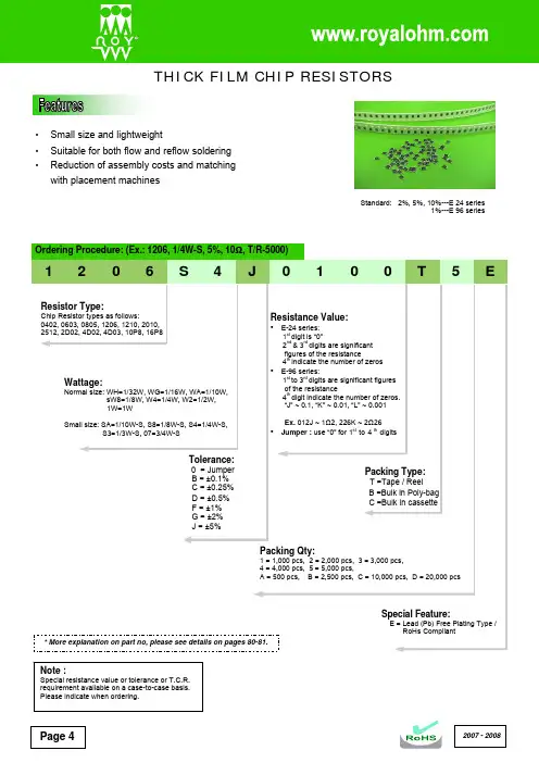
Page 4•Small size and lightweight• Suitable for both flow and reflow soldering •Reduction of assembly costs and matching with placement machines2007 - 2008Standard: 2%, 5%, 10%---E 24 series 1%---E 96 series2007 - 2008 Page 5Marking on the Resistors Body:•For 0402 size, no marking on the body due to the small size of the resistor.•±5% tolerance product. (Including resistance values less than 1Ω; both 1% and 5%) The marking is 3 digits, the first 2 digits are the significant figures of the resistance and the 3rd digit denotes number of zeros.153 = 15000Ω = 15KΩ; 120 = 12Ω Below 10Ω shown as this: 6R8 = 6.8Ω 0.1Ω~0.99Ω shown as this: R33 = 0.33Ω•±1% tolerance marking of case size 0805 and bigger is 4 digits, the first 3 digits are the significant figures of the resistance and the 4th digit denotes number of zeros.2372 = 23700Ω = 23.7KΩ; 1430 = 143Ω Below 10Ω shown as this: 3R24 = 3.24Ω0.1Ω~0.99Ω shown as this: R33 = 0.33ΩPage 62007 - 2008* More details, please see pages 78-79.• Standard E-96 series values (±1% tolerance) of 0603 size. Due to the small size of the resistor’s body, 3 digitsmarking will be used to indicate the accurate resistance value by using the Multiplier code & Standard E-96 Series Resistance Value Code as shown on Page 6.1.96K Ω = 196 x 101 Ω = 29B12.4Ω = 124 x 10-1 Ω = 10X• Standard E-24 series values which does not belong to E-96 series values (in ±1% tolerance) of 0603 size. The marking is the same as 5% tolerance but marked with underline.122 = 1200 = 1.2K Ω680 = 68ΩTemperature coefficient±5%: 1Ω ~ 10M Ω ≤ ±200PPM/°C±1%: 10Ω ~ 100Ω ≤ ±200PPM/°C; 101Ω ~ 1M Ω ≤ ±100PPM/°C Short-time overload ±5%: ±(2.0% + 0.1Ω) Max. ±1%: ±(1.0% + 0.1Ω) Max. Insulation resistanceMin. 1,000 Mega OhmDielectric withstanding voltageNo evidence of flashover, mechanical damage, arcing or insulation breakdown Terminal bending ±(1.0% + 0.05Ω) Max.Soldering heat Resistance change rate is ±(1.0% + 0.05Ω) Max. SolderabilityMin. 95% coverage Temperature cycling ±5%: ±(1.0% + 0.05Ω) Max. ±1%: ±(0.5% + 0.05Ω) Max. Humidity (Steady State) ±5%: ±(3.0% + 0.1Ω) Max. ±1%: ±(0.5% + 0.1Ω) Max. Load life in humidity±5%: ±(3.0% + 0.1Ω) Max. ±1%: ±(1.0% + 0.1Ω) Max. Load life±5%: ±(3.0% + 0.1Ω) Max.±1%: ±(1.0% + 0.1Ω) Max.* The values which are not of standard E-24 series (2% & 5%) and not of E-96 series (1%) could be offered on a case to case basis.2007 - 2008Page 72007 - 2008Page 8•16P8 (16Pin 8R)THICK FILM CHIP RESISTOR ARRAYS• High density 2, 4, 8 resistors in one small case (convex type) • Improvement of placement efficiency• Packaging is suitable for automatic placement machines • Superior solderability • Scalloped•2D02 (4Pin 2R)•4D02, 4D03 (8Pin 4R)•10P8 (10Pin 8R)Part No.StyleLWHℓ1ℓ2PQ2D02 (0402x2) 2D02 (4Pin 2R) 1.0 ± 0.1 1.0 ± 0.1 0.35 ± 0.1 0.17 ± 0.1 0.25 ± 0.1 0.65 ± 0.05 0.33 ± 0.1 4D02 (0402x4) 4D02 (8Pin 4R) 2.0 ± 0.1 1.0 ± 0.1 0.45 ± 0.1 0.2 ± 0.15 0.3 ± 0.15 0.5 ± 0.05 0.3 ± 0.05 4D03 (0603x4) 4D03 (8Pin 4R) 3.2 ± 0.2 1.6 ± 0.2 0.5 ± 0.1 0.3 ± 0.15 0.3 ± 0.15 0.8 ± 0.1 0.5 ± 0.15 16P8 16P8 (16Pin 8R) 4.0 ± 0.2 1.6 ± 0.15 0.45 ± 0.1 0.3 ± 0.15 0.4 ± 0.15 0.5 ± 0.05 0.3 ± 0.05 10P8 10P8 (10Pin 8R)3.2 ± 0.21.6 ± 0.150.55 ± 0.10.4 ± 0.10.3 ± 0.150.64 ± 0.050.35 ± 0.05Resistance RangePart No. StylePower Rating at 70ºC Max. Working Voltage Max. Overload VoltageDielectric With-standing VoltageOperated Temp. RangeF (±1%) E-96 seriesJ (±5%) E-24 seriesJumper Rated Current2D02 2D02 (4Pin2R) 1/16W 50V 100V 500V -55ºC~+155ºC - 10Ω~ 1M Ω - 4D02 4D02 (8Pin4R) 1/16W 50V 100V 500V -55ºC~+155ºC -10Ω~ 1M Ω -4D03 4D03 (8Pin4R) 1/16W 50V 100V 500V -55ºC~+155ºC 100Ω~560K Ω 10Ω~ 1M Ω 1A 16P8 16P8 (16Pin8R) 1/16W 50V 100V 100V -55ºC~+155ºC - 10Ω~ 1M Ω - 10P810P8 (10Pin8R)1/32W 25V 50V 50V -55ºC~+155ºC -33Ω~ 100K Ω -Note: Part number and ordering procedure the same as Thick Film Chip Resistors on Page 4.Standard: 2%, 5%, 10%---E 24 series 1%---E 96 series。
厦门昱电电子有限公司
规格承认书
产品名称:氧化锌压敏电阻器(陕西华星)
一、特点与用途
压敏电阻器是以氧化锌为主要原材料制造的半导体陶瓷元件,其电阻值随施加电压的变化而呈非线形变化。
具有体积小、通流量大等特点。
主要用于半导体器件保护、家用电器浪涌过电压保护、通信、测量仪器的过电压保护。
二、命名方法
MY G 20 G07 K 471
压敏电压
电压允许误差(±10%)
芯片直径
20系列
G型压敏电阻器
三、技术参数
注:1. 标准品05K 系列压敏电压在0.1mA 电压下测量,07K 、10K 、14K 、20K 系列压敏电压在1mA 电压下测量。
2. 05K 、07K 、10K 、14K 、20K 分别代表瓷片直径为 φ5mm 、φ7mm 、φ10mm 、 φ14mm 、φ20mm 。
3. K 代表压敏电压±10%,后面三位数字中个位数字代表0的个数。
四、外形尺寸
φ5系列
φ7系列
五、产品取得认证。
R 科聚G G Y、G N Y系列氧化锌压敏电阻保护器ZnO VOLT-SENSITIVE PROTECTORS安徽时代科聚电气有限公司ANHUI TIME KEJU Electric Co. Ltd.1.产品概述氧化锌压敏电阻器是一种具有优良限压特性(压敏特性)的非线性电阻器,被国内外广泛用作电气系统过电压抑制元件。
本公司(原中国科学院等离子体物理研究所电器设备厂)从20世纪70年代起从事压敏电阻材料、器件的研究及应用开发,是国际上首先将高能氧化锌压敏电阻用于大型发电机转子灭磁及过电压保护,并实现产品化的单位。
本公司已形成从电子系统到电力系统,从低压到高压全系列的防雷过电压保护产品,所开发的各类压敏电阻阀片均具有独立知识产权,产品曾多次获得国家及省、部级奖励。
根据过电压的特点和不同电器设备保护的需要,多年来我们对上千例各种过电压保护问题进行分析,采用最新的微粉压敏材料制成高能型和高压型氧化锌压敏电阻阀片,开发出GNY、GGY系列压敏电阻器。
该电阻器具有能量容量大、残压低、动作速度快、保护性能稳定、适用范围广、体积小、安装简单、无须维护等特点,是传统过电压保护器的和早期氧化锌压敏电阻器的更新换代产品。
1.1 GNY高能型压敏电阻器系列主要应用于同步电机或直流电机的励磁回路、各类大功率半导体变换装置如整流器、逆变器、变频器、开关电源、UPS等以及电力机车高压变压器、三相电力变压器低压侧、大电感负载换流回路等大能量、宽脉冲过电压保护。
1.2 GGY高压型压敏电阻器系列主要用于抑制电气系统的各类操作过电压、回路谐振过电压和雷电感应过电压,还可用于大电流开关、接触器等的灭弧。
产品品种齐全,型式多样,不仅广泛应用于上述强电系统,还普遍用作电子设备、仪器、家电等过电压保护元件,保护性能稳定可靠。
2. 使用要求使用环境:温度不超过-40°C~+45°C,相对湿度在+40°C时不超过95%;使用场所:户内使用,一般安装于电气柜内。
关于压敏电阻的正确使用一、压敏电阻的原理压敏电阻意思是"在一定电流电压范围内电阻值随电压而变",或者是说"电阻值对电压敏感"的阻器。
相应的英文名称叫“Voltage Dependent Resistor”简写为“VDR”。
随着加在它上面的电压不断增大,它的电阻值可以从MΩ(兆欧)级变到mΩ(毫欧)级。
当电压较低时,压敏电阻工作于漏电流区,呈现很大的电阻,漏电流很小;当电压升高进入非线性区后,电流在相当大的范围内变化时,电压变化不大,呈现较好的限压特性;电压再升高,压敏电阻进入饱和区,呈现一个很小的线性电阻,由于电流很大,时间一长就会使压敏电阻过热烧毁甚至炸裂。
正常使用时压敏电阻处于漏电流区,受到浪涌冲击时进入非线性区泄放浪涌电流,一般不能进入饱和区压敏电阻器的电阻体材料是半导体,所以它是半导体电阻器的一个品种。
现在大量使用的"氧化锌"(ZnO)压敏电阻器,它的主体材料有二价元素(Zn)和六价元素氧(O)所构成。
所以从材料的角度来看,氧化锌压敏电阻器是一种“Ⅱ-Ⅵ族氧化物半导体”。
二、压敏电阻的作用压敏电阻的最大特点是当加在它上面的电压低于它的阀值"UN"时,流过它的电流极小,相当于一只关死的阀门,当电压超过UN时,流过它的电流激增,相当于阀门打开。
利用这一功能,可以抑制电路中经常出现的异常过电压,保护电路免受过电压的损害。
压敏电阻器是一种具有瞬态电压抑制功能的元件,可以用来代替瞬态抑制二极管、齐纳二极管和电容器的组合。
压敏电阻器可以对IC 及其它设备的电路进行保护,防止因静电放电、浪涌及其它瞬态电流(如雷击等)而造成对它们的损坏。
使用时只需将压敏电阻器并接于被保护的IC 或设备电路上,当电压瞬间高于某一数值时,压敏电阻器阻值迅速下降,导通大电流,从而保护IC 或电器设备;当电压低于压敏电阻器工作电压值时,压敏电阻器阻值极高,近乎开路,因而不会影响器件或电器设备的正常工作。