SP1117-3.3V使用手册
- 格式:pdf
- 大小:284.21 KB
- 文档页数:10


LDO1117-3.3VTECHNICAL DATA1.0A Low Dropout Positive Voltage RegulatorThe IL1117 is a series of low dropout voltage regu-lators which can provide up to 1A of output current. The IL1117 is available in eight fixed voltage, 1.2, 1.25, 1.5,1.8, 2.5, 2.85, 3.3 and 5.0V. Additionally it is also avail-able in adjustable version. On chip precision trimming adjusts the reference/ output voltage to withined(for IL1117-1.2V - 0 to +150°C)Applications●Post Regulator for switching DC/DC Converter ● High Efficiency Linear Regulator ● Battery Chargers ● PC Add on Card● Motherboard clock supplies ● LCD Monitor ● Set-top BoxAbsolute Maximum RatingsSymbol DescriptionMax Units VIN Input Voltage15V IOUT DC Output CurrentPD/(VIN-VO)mA TJ Operating Junction Temperature Range -40 to 125°C ΘJA Thermal Resistance (SOT-223)150°C/W ΘJA Thermal Resistance (TO-252)80°C/W ΘJA Thermal Resistance (TO-220)60°C/W PD Maximum Power Dissipation (SOT-223)mW PD Maximum Power Dissipation (TO-252)mW PDMaximum Power Dissipation (SOT-220)Internally LimitedIL1117-xxPin#2 connected with heat sinkElectrical CharacteristicsVin = 5V, Co = 10uF, Ta = 25°C, Tj = -40°C to +125°C ( for IL1117-1.2 Tj = 0 to +150°C) unless otherwise specified PARAMETER CONDITIONS MIN TYP MAX UNIT OUTPUT VOLTAGEIL1117-1.2IL1117-1.25 (Adjustable)IL1117-1.5IL1117-1.8IL1117-2.5IL1117-2.85IL1117-3.3IL1117-5.0Io = 10mA to 1.0A, Vin = 2.7 to 12.0VIo = 10mA to 1.0A, Vin = 2.8 to 12.0VIo = 10mA to 1.0A, Vin = 3.0 to 12.0VIo = 10mA to 1.0A, Vin = 3.3 to 12.0VIo = 10mA to 1.0A, Vin = 4.0 to 12.0VIo = 10mA to 1.0A, Vin = 4.4 to 12.0VIo = 10mA to 1.0A, Vin = 4.8 to 12.0VIo = 10mA to 1.0A, Vin = 6.5 to 15.0V1.1761.2251.4701.7642.4502.7903.2401.2001.2501.5001.8002.5002.8503.3005.0001.2241.2801.5301.8362.5502.9103.3605.100VLINE REGULATIONIL1117-1.2IL1117-1.25 (Adjustable)IL1117-1.5IL1117-1.8IL1117-2.5IL1117-2.85IL1117-3.3IL1117-5.0Io =10mA, Vin = 2.7 to 12.0V Io =10mA, Vin = 2.8 to 12.0VIo =10mA, Vin = 3.0 to 12.0VIo =10mA, Vin = 3.3 to 12.0VIo =10mA, Vin = 4.0 to 12.0V Io =10mA, Vin = 4.4 to 12.0V Io =10mA, Vin = 4.8 to 12.0V Io =10mA, Vin = 6.5 to 15.0V 2.00.12.02.02.02.03.04.07.00.27.07.07.07.07.010.0mV%mVmVmVmVmVmVLOAD REGULATIONIL1117-1.2IL1117-1.25 (Adjustable)IL1117-1.5IL1117-1.8IL1117-2.5IL1117-2.85IL1117-3.3IL1117-5.0Io = 10mA to 1.0A, Vin = 3.2V Io = 10mA to 1.0A, Vin = 3.3VIo = 10mA to 1.0A, Vin = 3.5VIo = 10mA to 1.0A, Vin = 3.8VIo = 10mA to 1.0A, Vin = 4.5VIo = 10mA to 1.0A, Vin = 4.85VIo = 10mA to 1.0A, Vin = 5.3VIo = 10mA to 1.0A, Vin = 7.0V3.00.23.03.03.03.04.05.010.00.410.010.010.010.012.015.0mV%mVmVmVmVmVmVDROPOUT VOLTAGE(2)All Models Io =1A 1.20 1.30VIo Tj =-40°C to +125°C) 1.20 1.55 CURRENT LIMIT Vin - Vo = 5V1000mA MINIMUM LOAD CURRENTAdjustable Models Vin= 13.75V5mA QUIESCENT CURRENT Vin - Vo = 1.5V 5.210mA Adjust Pin Current Io = 10mA, Vin - Vo = 1.4 to 10V50120uA vs Load Current,IL1117Io= 10mA to 1A,Vin Vo= 1.4 to 10V0.55uA TEMPERATURE DRIFT Tj = -40°C to +125°C0.5% RMS Output Noise Bandwidth of 10Hz to 10kHz at 25°C0.003%VoRipple Rejection Ratio 120Hz input Ripple(Cadj for ADJ) =25uFVin -Vo= 5V, Io = 1.0ATj = -40°C to +125°C6072dBNOTES: (1) IL1117-x adjustable versions require a minimum load current for ±3% regulation.(2) Dropout voltage is the input voltage minus output voltage that produces a 1% decrease inoutput voltage.Block DiagramApplication InformationFIGURE 1. Fixed-Voltage Model FIGURE 2. Adjustable-Voltage Model—Basic Connections. --Basic Connections.Vo=Vref(1+R2/R1)+Iadj*R2IL1117IL1117(Adj)Typical Perfomance CharacteristicsTypical Perfomance Characteristics (continue)Figure 3.Application InformationOutput voltage adjustmentLike most regulators, the IL1117 regulates the output by comparing the output voltage to an internally gen-erated reference voltage. On the adjustable version as shown in Fig.4, the V REF is available externally as 1.25V between V OUT and ADJ.The voltage ratio formed by R1 and R2 should be set to conduct 10mA (mi-numum output load).The output voltage is given by the following equation:On fixed versions of IL1117, the voltage divider is provided internally.Figure 4. Basic Adjustable RegulatorInput Bypass CapacitorAn input capacitor is recommended. A 10μF tantalum on the input is a suitable input bypassing for almost all applications.Adjust Terminal Bypass CapacitorThe adjust terminal can be bypassed to ground with a bypass capacitor (C ADJ) to improve ripple rejection. This bypass capacitor prevents ripple from being amplified as the output voltage is increased. At any ripple frequency, the impedance of the C ADJ should be less than R1 to prevent the ripple from being amplified:The R1 is the resistor between the output and the adjust pin. Its value is normally in the range of 100- 200Ω. For example, with R1 = 124Ωand f RIPPLE= 120Hz, the C ADJ should be> 11μF.Output CapacitorIL1117 requires a capacitor from V OUT to GND to providecompensation feedback to the internal gain stage. This is to ensure stability at the output terminal. Typically, a 10μF tantalum or 50μF aluminum electrolytic is sufficient.Note: It is important that the ESR for this capacitor does not exceed 0.5 Ω.The output capacitor does not have a theoretical upper limit and increasing its value will increase stability.C OUT= 100μF or more is typical for high current regulator design.Load RegulationWhen the adjustable regulator is used (Fig.5), the best load regulation is accomplished when the top of the resistor divider (R1) is connected directly to the output pin of the IL1117. When so connected, R P is not multiplied by the divider ratio. For Fixed output version, the top of R1 is internally connected to the output and ground pins can be connected to low side of the load.Figure 5. Best Load Regulation Using Adjustable Output RegulatorThermal ProtectionIL1117 has thermal protection which limits junction tempe rature to 150°C. However, device functionality is only guaranteed to a maximum junction temperature of +125°C. The power dissipation and junction tem-perature for IL1117 in DPAKpackage are given byNote: T JUNCTION must not exceed 125°CCurrent Limit ProtectionIL1117 is protected against overload conditions. Current protection is triggered at typically 1.6A.Thermal ConsiderationThe IL1117 series contain thermal limiting circuitry designed to protect itself from over-temperature condi-tions. Even for normal load conditions, maximum junction temperature ratings must not be exceeded. As mention in thermal protection section, we need to consider all sources of thermal resistance between junc-tion and ambient. It includes junction-tocase, case-to-heat-sink interface, and heat sink thermal resistance itself.Junction-to-case thermal resistance is specified from the IC junction to the bottom of the case directly below the die. Proper mounting is required to ensure the best possible thermal flow from this area of the package to the heat sink. The case of all devices in this series is electrically connected to the output. Therefore, if the case of the device must be electrically isolated, a thermally conductive spacer is recommended.。
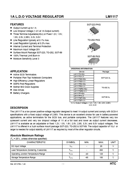
DESCRIPTIONFEATURES■ Guaranteed 0.8A Output Current ■ Guaranteed 1A Peak Current■ Three Terminal Adjustable or Fixed 1.5V, 1.8V, 2.5V, 2.85V, 3.0V, 3.3V and 5V■ Low Quiescent Current■ Low Dropout Voltage of 1.1V at 0.8A ■ 0.1% Line and 0.2% Load Regulation ■ Stable with 2.2uF Ceramic Capacitor ■ Overcurrent and Thermal Protection ■ Available Packages: SOT-223,TO-252, TO-220, and TO-263The SPX1117 is a low power positive-voltage regulator designed to satisfy moderate power requirements with a cost effective, small footprint solution. This device is an excellent choice for use in battery-powered applications and portable computers. The SPX1117 features very low quiescent current and a low dropout voltage of 1.1V at a full load. As output current decreases,quiescent current flows into the load, increasing efficiency. SPX1117 is available in adjustable or fixed 1.5V, 1.8V, 2.5V,2.5V, 2.85V, 3.0V, 3.3V and 5V output voltages.The SPX1117 is offered in several 3-pin surface mount packages: SOT-223, TO-252, TO-220and TO-263. An output capacitor of 10µF provides unconditional stability while a smaller 2.2µF capacitor is sufficient for most applications.APPLICATIONS■ Desktop PC's Servers ■ SCSI-II Active Terminator■ Portable/ Palm Top / Notebook Computers■ Cordless Phones ■ Battery Chargers ■ Disk Drives■ Portable Consumer Equipment ■ Portable Instrumentation ■ SMPS Post-RegulatorFUNCTIONAL DIAGRAMOUTINµANow Available in Lead Free PackagingELECTRICAL CHARACTERISTICSTA = 25°C, CIN= COUT= 10µF, unless otherwise specified. The Boldface applies over the full operating temperature range.PARAMETER CONDITIONS MIN TYP MAX UNITS 1.5V VersionOutput Voltage IOUT = 10mA, VIN=3.0V, TJ= 25ºC 1.485 1.500 1.515V10mA ≤ IOUT ≤ 800mA, 2.9V ≤ VIN≤ 10V 1.470 1.5301.8V VersionOutput Voltage IOUT = 10mA, VIN=3.3V, TJ= 25ºC 1.782 1.800 1.818V10mA ≤ IOUT ≤ 800mA, 3.2V ≤ VIN≤ 10V 1.764 1.8362.5V VersionOutput Voltage IOUT = 10mA, VIN=4.0V, TJ= 25ºC 2.475 2.500 2.525V10mA ≤ IOUT ≤ 800mA, 3.9V ≤ VIN≤ 10V 2.450 2.5502.85V VersionOutput Voltage IOUT = 10mA, VIN=4.35V, TJ= 25ºC 2.821 2.850 2.878V10mA ≤ IOUT ≤ 800mA, 4.25V ≤ VIN≤ 10V 2.793 2.9073.00V VersionOutput Voltage IOUT = 10mA, VIN=4.5V, TJ= 25ºC 2.970 3.000 3.030V10mA ≤ IOUT ≤ 800mA, 4.4V ≤ VIN≤ 10V 2.940 3.0603.30V VersionOutput Voltage IOUT = 10mA, VIN=4.8V, TJ= 25ºC 3.267 3.300 3.333V10mA ≤ IOUT ≤ 800mA, 4.7V ≤ VIN≤ 10V 3.234 3.3665V VersionOutput Voltage IOUT = 10mA, VIN=6.5V 4.9505 5.050V10mA ≤ IOUT ≤ 800mA, 6.4V ≤ VIN≤ 12V 4.90 5.10All Voltage OptionsReference Voltage IOUT =10mA, (VIN- VOUT)= 2V, TJ= 25ºC 1.238 1.250 1.262V10mA≤IOUT ≤ 800mA, 1.4V≤(VIN-VOUT)≤ 10V 1.225 1.270Output Voltage0.3% Temperature StabilityLine Regulation VINMIN ≤VIN≤ 12V,VOUT=Fixed/Adj,(Note 1)IOUT=10mA37mVLoad Regulation10mA≤IOUT ≤ 800mA,VOUT=Fixed/Adj612mV(Note 1)Dropout Voltage IOUT =100mA 1.00 1.10V(Note 2)IOUT =500mA 1.05 1.15IOUT=800mA 1.10 1.20Quiescent Current 4.25V≤VIN ≤ 6.5V510mAPower Dissipation.......................................Internally Limited Lead Temperature (soldering, 5 seconds) ...............260°C Storage Temperature Range.......................-65°C to +150°C Operating Junction Temperature Range.....-40°C to +125°C Input Supply Voltage....................................................+20V Input to Output Voltage................................................18.8V ESD Rating.................................................................2kV min These are sterss ratings only and functional operation of the device at these ratings or any other above those indicated in the operation sections of the specifications below is not implied. Exposure to absolute maximum rating conditions for extended periods of time may affect reliability.ABSOLUTE MAXIMUM RATINGSELECTRICAL CHARACTERISTICST A = 25°C, C IN = C OUT = 10µF, unless otherwise specified. The Boldface applies over the full operating temperature range.PARAMETER CONDITIONS MIN TYP MAX UNITS Adjust Pin Current 50120µA Current Limit (V IN -V OUT )=5V 1.01.52.0A Thermal Regulation 25°C, 30mS pulse0.010.1%/W Ripple Rejection f RIPPLE =120Hz, (V IN -V OUT )=2V,6075dB V RIPPLE =1V PP Long Term Stability 125°C, 1000Hrs0.03%RMS Output Noise % of V OUT , 10Hz ≤f ≤10kHz0.003%Thermal ResistanceTO-220 Junction to Case, at Tab 3°C/WTO-220 Junction to Ambient 60TO-263 Junction to Case, at Tab 3TO-263 Junction to Ambient 60TO-252 Junction to Case, at Tab 6TO-252 Junction to Ambient126SOT-223 Junction to Case, at Tab 15SOT-223 Junction to Ambient156*Note 1 - For fixed option, V INMIN = V OUT + 1.5V- For adjustable option, V INMIN = V IN - V OUT = 1.4V*Note 2 - Dropout voltage is the input voltage minus output voltage that produces a 1% decrease in output voltage with respect to the nominal output voltage at V IN = V OUT + 1.5VTYPICAL PERFORMANCE CHARACTERISTICSFigure 1. Load Regulation for SPX1117M3-3.3;Figure 2. Line Regulation for SPX1117M3-3.3; V IN =4.8V I OUT =10mAFigure 3. Dropout Voltage vs Output Current for SPX1117M3-3.3; V IN =4.8V, C OUT =2.2µFVoltage Deviation with I OUT =10mA to 1A StepFigure 6. V OUT vs Temperature, V IN =2.5V, I OUT =10mAIN C IN =C OUT =1µF, I OUT pulsed from 10mA to Current LimitIN OUTIN OUTIN OUT TYPICAL PERFORMANCE CHARACTERISTICS: ContinuedFigure 8. V IN =3.3V, I OUT =10mAIN OUT IN OUT Figure 14. Output Voltage vs Temperature at different Current Loads, V IN =3.3V, V OUT = 1.8V AdjustableFigure 13. Line Regulation vs Temperature. V OUT =1.8V (adjustable), V IN = 3.3VFigure 15. Line Regulation at I LOAD =800mA over Temperature, V OUT =1.8V adjustableOutput CapacitorTo ensure the stability of the SPX1117, anoutput capacitor of at least 2.2µF (tantalum orceramic) or 10µF (aluminum) is required. The value may change based on the application requirements of the output load or temperature range. The value of ESR can vary based on the type of capacitor used in the applications to guarantee stability. The recommended value for ESR is 0.5Ω or less. A larger value of output capacitance (up to 100µF) can improve the load transient response.Soldering MethodsThe SPX1117 SOT-223 package is designed to be compatible with infrared reflow or vapor-phase reflow soldering techniques.During soldering, the non-active or mildly active fluxes may be used. The SPX1117 die is attached to the heatsink lead which exits opposite the input, output, and ground pins.Hand soldering and wave soldering should be avoided since these methods can causedamage to the device with excessive thermal gradients on the package. The SOT-223recommended soldering method are as follows: vapor phase reflow and infraredreflow with the component preheated to within 65°C of the soldering temperature range.Figure 16. Load Step Response (0 to 800mA), Vin=3.3V,Vout=1.8V, Cin=10µF, Cout=2.2µF, Ceramic; 1 = Vout,4= IloadFigure 17. Load Step Response (0 to 800mA), Vin=3.3V,Vout=1.8V, Cin=10µF, Cout=2.2µF, OSCON; 1 = Vout,4= IloadAPPLICATION INFORMATIONThermal CharacteristicsThe thermal resistance of SPX1117 (SOT-223Package) is 15°C/W from junction to tab and 31°C/W from tab to ambient for a total of 46 °C/W from junction to ambient (Table 1). The SPX1117features the internal thermal limiting to protect the device during overload conditions. Special care needs to be taken during continuous load conditions such that the maximum junction tem-perature does not exceed 125 °C. Thermal pro-tection is activated at >155°C and deactiviated at <140 °C.Taking the FR-4 printed circuit board and 1/16thick with 1 ounce copper foil as an experiment (fig.13), the PCB material is effective at trans-mitting heat with the tab attached to the pad area and a ground plane layer on the backside of the substrate. Refer to table 1 for the results of the experiment.The thermal interaction from other components in the application can effect the thermal resis-tance of the SPX1117. The actual thermal resistance can be determined with experimenta-tion.SPX1117 power dissipation is calculated as follows:P D = (V IN - V OUT )(I OUT )Maximum Junction Temperature range:T J = T A (max) + P D * thermal resistance (junction-to-ambient)Maximum junction temperature must not ex-ceed the 125°C.Ripple RejectionRipple rejection can be improved by adding a capacitor between the ADJ pin and ground as shown in Figure 23. When ADJ pin bypassing is used, the value of the output capacitor re-quired increases to its maximum. If the ADJ pin is not bypassed, the value of the output capacitor can be lowered to 10µF for an electrolytic alu-minum capacitor or 2.2µF for a ceramic or solid tantalum capacitor (Fig 22).However the value of the ADJ-bypass capacitor should be chosen with respect to the following equation:C = 1 / ( 6.28 * F R * R 1 )WhereC = value of the capacitor in Farads (select an equal or larger standard value),F R = ripple frequency in Hz,R 1 = value of resistor R1 in Ohms.If an ADJ-bypass capacitor is used, the ampli-tude of the output ripple will be independent of the output voltage. If an ADJ-bypass capacitor is not used, the output ripple will be proportional to the ratio of the output voltage to the reference voltage:M = V OUT / V REF Where M = multiplier for the ripple seen when the ADJ pin is optimally bypassed.V REF =1.25VRipple rejection for the adjustable version is shown in Figure 20.Figure 19. Substrate Layout for SOT-223Figure 20. Ripple Rejection; Vin=3.3V, Vout=1.8V (adj.), Iload=200mAAPPLICATION INFORMATION: ContinuedOutput VoltageThe output of the adjustable regulator can be set to any voltage between 1.25V and 15V. The value of V OUT can be quickly approximated using the formulaV OUT =1.25 *(R 1 + R 2)/R 1.A small correction to this formula is required depending on the values of resistors R 1 and R 2,since the adjustable pin current (approx 50µA)flows through R 2. When I ADJ is taken into ac-count, the formula becomesPC BOARD TOPSIDE COPPER BACKSIDE COPPER THERMAL RESISTANCEJUNC. TO AMB.mm 2mm 2mm 2°C/W25002500250046 25001250250047 2500950250049 25002500051 250018000531600600160055250012500582500915059160060006790024090072900240085V OUT = V REF (1+ (R 2/R 1)) + I ADJ * R 2,whereV REF =1.25V.Layout ConsiderationsParasitic line resistance can degrade load regu-lation. In order to avoid this, connect R 1 directly to V OUT as illustrated in Figure 25. For the same reason, R 2 should be connected to the negative side of the load.Figure 21. Current Source Figure 22. Typical Adjustable RegulatorTABLE 1APPLICATION INFORMATION: ContinuedAPPLICATION INFORMATION: ContinuedPINOUTS SOT-223 (M3)Top ViewTO-263-3 (T)Front ViewTO-220-3 (U)Front ViewTO-252 (R)ADJ/GND VOUTVINADJ/GND VOUTVINADJ/GND VOUTVINADJ/GND VOUTVINTop ViewPACKAGE: 3 PIN SOT-223Section C-C- - 1.800.02 - 0.10Dimensions in (mm)3 PIN SOT-223JEDEC TO-261(AA) V ariation6.506.707.00 7.30A A1D E E1e LMIN NOM MAX c 0.230.300.356.306.70ø0º-10ºA2 1.50 1.60 1.700.66 0.76 0.84b b2 2.90 3.00 3.103.30 3.50 3.702.30 BASIC e1 4.60 BASIC 0.75 - -3 PIN SOT-223PACKAGE: 3 PIN TO-2521PACKAGE: 3 PIN TO-220.140 - .190.020 - .055Dimensions in (mm)3 PIN TO-220JEDEC TO-220(AB) V ariation.080 - .115.015 .027 .040.015 - .038.045 - .070.014 - .022 .480 - .507A A1A2b b1b2b3c1D1D2 .380 - .420E MIN NOM MAX.045 - .068c .014 - .024D .560 - .650.330 - .355E1.270-.350E2- - .030e .100 BSC e1.200 BSCN 4H1.230 - .270L1- - .250L2- - -∆P .139 - .161Q.100 - .135PACKAGE: 3 PIN TO-263(4.4700.127)±(1.2700.051)±ORDERING INFORMATION PART NUMBER ACC. OUTPUT VOLTAGE PACKAGE SPX1117M3.................................1%......................................Adj..........................3 Pin SOT-223 SPX1117M3/TR...........................1%......................................Adj..........................3 Pin SOT-223 SPX1117M3-1.5...........................1%.....................................1.5V.........................3 Pin SOT-223 SPX1117M3-1.5/TR.....................1%.....................................1.5V.........................3 Pin SOT-223 SPX1117M3-1.8...........................1%.....................................1.8V.........................3 Pin SOT-223 SPX1117M3-1.8/TR.....................1%.....................................1.8V.........................3 Pin SOT-223 SPX1117M3-2.5...........................1%.....................................2.5V.........................3 Pin SOT-223 SPX1117M3-2.5/TR.....................1%.....................................2.5V.........................3 Pin SOT-223 SPX1117M3-2.85.........................1%....................................2.85V........................3 Pin SOT-223 SPX1117M3-2.85/TR...................1%....................................2.85V........................3 Pin SOT-223 SPX1117M3-3.0...........................1%.....................................3.0V.........................3 Pin SOT-223 SPX1117M3-3.0/TR.....................1%.....................................3.0V.........................3 Pin SOT-223 SPX1117M3-3.3...........................1%.....................................3.3V.........................3 Pin SOT-223 SPX1117M3-3.3/TR.....................1%.....................................3.3V.........................3 Pin SOT-223 SPX1117M3-5.0...........................1%.....................................5.0V.........................3 Pin SOT-223 SPX1117M3-5.0/TR.....................1%.....................................5.0V.........................3 Pin SOT-223 SPX1117R...................................1%......................................Adj.............................3 Pin TO-252 SPX1117R/TR.............................1%......................................Adj.............................3 Pin TO-252 SPX1117R-1.5.............................1%.....................................1.5V............................3 Pin TO-252 SPX1117R-1.5/TR.......................1%.....................................1.5V............................3 Pin TO-252 SPX1117R-1.8.............................1%.....................................1.8V............................3 Pin TO-252 SPX1117R-1.8/TR.......................1%.....................................1.8V............................3 Pin TO-252 SPX1117R-2.5.............................1%.....................................2.5V............................3 Pin TO-252 SPX1117R-2.5/TR.......................1%.....................................2.5V............................3 Pin TO-252 SPX1117R-2.85...........................1%....................................2.85V...........................3 Pin TO-252 SPX1117R-2.85/TR.....................1%....................................2.85V...........................3 Pin TO-252 SPX1117R-3.0.............................1%.....................................3.0V............................3 Pin TO-252 SPX1117R-3.0/TR.......................1%.....................................3.0V............................3 Pin TO-252 SPX1117R-3.3.............................1%.....................................3.3V............................3 Pin TO-252 SPX1117R-3.3/TR.......................1%.....................................3.3V............................3 Pin TO-252 Available in lead free packaging. To order add "-L" suffix to part number.Example: SPX1117M3-5.0/TR = standard; SPX1117M3-L-5.0/TR = lead free/TR = Tape and ReelPack quantity is 500 for TO-263, 2,000 for TO-252, and 2,500 for SOT223.ANALOG EXCELLENCEHeadquarters andSales Office233 South Hillview DriveMilpitas, CA 95035TEL: (408) 934-7500FAX: (408) 935-7600Sipex Corporation reserves the right to make changes to any products described herein. Sipex does not assume any liability arising out of the application or use of any product or circuit described herein; neither does it convey any license under its patent rights nor the rights of others.ORDERING INFORMATION PART NUMBER ACC. OUTPUT VOLTAGE PACKAGE SPX1117T....................................1%......................................Adj.............................3 Pin TO-263 SPX1117T/TR..............................1%......................................Adj.............................3 Pin TO-263 SPX1117T-1.5.............................1%.....................................1.5V............................3 Pin TO-263 SPX1117T-1.5/TR........................1%.....................................1.5V............................3 Pin TO-263 SPX1117T-1.8.............................1%.....................................1.8V............................3 Pin TO-263 SPX1117T-1.8/TR........................1%.....................................1.8V............................3 Pin TO-263 SPX1117T-2.5.............................1%.....................................2.5V............................3 Pin TO-263 SPX1117T-2.5/TR........................1%.....................................2.5V............................3 Pin TO-263 SPX1117T-2.85...........................1%....................................2.85V...........................3 Pin TO-263 SPX1117T-2.85/TR......................1%....................................2.85V...........................3 Pin TO-263 SPX1117T-3.0.............................1%.....................................3.0V............................3 Pin TO-263 SPX1117T-3.0/TR........................1%.....................................3.0V............................3 Pin TO-263 SPX1117T-3.3.............................1%.....................................3.3V............................3 Pin TO-263 SPX1117T-3.3/TR........................1%.....................................3.3V............................3 Pin TO-263 SPX1117U...................................1%......................................Adj..............................3 Pin TO220 SPX1117U-1.5.............................1%.....................................1.5V.............................3 Pin TO220 SPX1117U-1.8.............................1%.....................................1.8V.............................3 Pin TO220 SPX1117U-2.5.............................1%.....................................2.5V.............................3 Pin TO220 SPX1117U-2.85...........................1%....................................2.85V............................3 Pin TO220 SPX1117U-3.0.............................1%.....................................3.0V.............................3 Pin TO220 SPX1117U-3.3.............................1%.....................................3.3V.............................3 Pin TO220 Available in lead free packaging. To order add "-L" suffix to part number.Example: SPX1117M3-5.0/TR = standard; SPX1117M3-L-5.0/TR = lead free/TR = Tape and ReelPack quantity is 500 for TO-263, 2,000 for TO-252, and 2,500 for SOT223.Sipex CorporationHeadquarters andSales Office233 South Hillview DriveMilpitas, CA 95035TEL: (408) 934-7500FAX: (408) 935-7600This datasheet has been downloaded from:Free DownloadDaily Updated Database100% Free Datasheet Search Site100% Free IC Replacement Search SiteConvenient Electronic DictionaryFast Search SystemAll Datasheets Cannot Be Modified Without PermissionCopyright © Each Manufacturing Company。
1A Adjustable/Fixed Low Dropout Linear Regulator- Low dropout voltage- Load regulation: 0.2% typical - Optimized for Low V oltage - On-chip thermal limiting- Standard SOT-223 and TO-252 packages- Three-terminal adjustable or fixed low dropout 1.2V ,1.5V ,1.8V , 2.5V , 2.85V , 3.3V , 5V . Regulators- Active SCSI terminators- High efficiency linear regulators- Post regulators for switching supplies - Battery chargers- 12V to 5V linear regulators - M otherboard clock suppliesThe AMS 1117-ADJ and AMS 1117-1.2,-1.5,-1.8,-2.5,-2.85, -3.3 and-5 are low dropout three-terminal regulators with 1A output current capability. These devices have been optimized for low voltage where transient response and minimum input voltage are critical. The 2.85V version is designed specifically to be used in Active Terminators for SCSI bus.On-chip thermal limiting provides protection against any combination of overload and ambient temperatures that would create excessive junction temperatures.Unlike PNP type regulators where up to 10% of the output current is wasted as quiescent current, the quiescent cur-rent of the AMS 1117 flows into the load, increasing effi-ciency.The AMS 1117 series regulators are available in the indus-try-standard SOT-223 and TO-252 power packages.Key FeaturesApplicationsGeneral DescriptionTypical ApplicationNotice: The distance between V out pin and Capacitor should not exceed 4cm for excellent performanceFigure 1. Typical Applications of AMS 11171A Adjustable/Fixed Low Dropout Linear RegulatorPin Assignments*With package soldered to 0.5 square inch copper area over backside ground plane or internal power plane, ΘJA can vary from 30°C/W to more than 50°C/W. Other mounting techniques may provide better thermal resistance than 30°C/W.Absolute Maximum RatingsFigure 2. Pin Assignments of AMS 1117ParameterMin.Max.UnitV IN 18 V(V IN – V OUT ) * I OUTSee Figure 3Operating Junction Temperature Range -20 125°C Storage Temperature Range-65150°C Lead Temperature (Soldering, 10 sec.) 300°C1A Adjustable/Fixed Low Dropout Linear RegulatorTypicals and limits appearing in normal type apply for T J =25℃.Limits appearing in Boldface type apply over the entire junction temperature for operation, -20℃to 125℃.Electrical CharacteristicBlock DiagramThermal LimitCurrent LimitV OUTV INSubstrateGND (fixed output) ADJ. (adjustable output)Figure 3. Block Diagram of AMS 1117Symbol ParameterConditionsMin (Note 2) Typ (Note 1) Max(Note 2)UnitsV REFReference VoltageAMS 11171.5V<=(V IN -V OUT )<=7V,10mA<=I OUT <=1A1.225 1.250 1.275 VV OUT OutputVoltage 10mA<=I OUT <=1AI OUT = 10mA, V IN = 3.2V AMS 1117-1.2 ,2.7V<= V IN <=8.2V 1.176 1.152 1.200 1.200 1.224 1.248 V AMS 1117-1.5 ,3.0V<= V IN <=8.5V1.4701.5001.530VAMS 1117-1.8 ,3.3V<= V IN <=8.8V 1.764 1.800 1.836 VAMS 1117-2.5 ,4V<= V IN <= 9.5V 2.450 2.500 2.550 V AMS 1117-2.85 , 4.35V <= V IN <= 9.85V 2.793 2.850 2.907 V AMS 1117-3.3 , 4.8V<= V IN <=10.3V 3.234 3.300 3.366 V AMS 1117-5.0,6.5V<=V IN <= 12V4.9005.0005.100V1A Adjustable/Fixed Low Dropout Linear RegulatorTypicals and limits appearing in normal type apply for T J =25℃.Limits appearing in Boldface type apply over the entire junction temperature for operation, -20℃ to 125℃.Electrical Characteristic(Continued)SymbolParameter ConditionsMin (Note 2)Typ (Note 1) Max (Note 2) Units △V OUTLine Regultion (Note 3)I OUT =10mA ,(V OUT +1.5V)<=V IN <=12V 0.035 0.2 % Load Regultion (Note 3) V IN -V OUT =2V,10mA<= I OUT <=1A,0.2 0.7 % AMS 1117-1.2V IN -V OUT =2V,10mA<= I OUT <=1A,0.2 1 % V IN -V OUTDropout Volage I OUT =1A,△V REF =1% 1.100 1.250 V I LimitCurrent Limit V IN -V OUT = 2V, T J =25℃1.1 1.5A Minimum Load Current (Note 4) AMS 1117-ADJ1.5V<=(V IN -V OUT )<=10V10mA Quiescent CurentV IN =V OUT +1.25V 5 13 mA Thermal Regulation T A = 25°C, 30ms pulse 0.01 0.1 %/W RippleRejection f=120Hz,V IN -V OUT =3V, V Ripple =1V PP60 72 dB Adjust Pin Current50120µAAdjust Pin CurrentChange 1.5V<=V IN -V OUT <=7V, 10mA<=I OUT <=1A0.2 5 µATemperature Stability0.5 % Long Term StabilityT A = 125°C, 1000hrs.0.3%1A Adjustable/Fixed Low Dropout Linear RegulatorNote 1: Typical Values represent the most likely parametric norm. Note 2: All limits are guaranteed by testing or statistical analysis.Note 3: Load and line regulation are measured at constant junction room temperature. Note 4: The minimum output current required to maintain regulation.Typical Performance CharacteristicsTypicals and limits appearing in normal type apply for T J =25℃.Limits appearing in Boldface type apply over the entire junction temperature for operation, -20℃to 125℃.Electrical Characteristic(Continued)Symbol ParameterConditionsMin (Note 2) Typ (Note 1) Max (Note 2)UnitsI LimitRMS Output Noise(% ofV OUT )T A = 25°C, 10Hz<= f <=10kHz0.003 % Thermal Resistance, Junctionto CaseSOT-223 15 ℃/W TO-252 3 ℃/W Thermal Shutdown Junction Temperature155 ℃ Thermal Shutdown Hysteresis25℃Output Current ( A )0 0.2 0.4 0.6 0.8 1.01.5 1.4 1.3 1.2 1.0 0.9 0.8 0.7 0.6 0.5 0D r o p o u t V o l t a g e ( V )Figure 4. Dropout Voltage VS. Output Current1A Adjustable/Fixed Low Dropout Linear RegulatorTypical Performance Characteristics(Continued)Figure 6. Output Voltage VS. TemperatureO u t p u t V o l t a g e ( V )3.70 3.65 3.60 3.55 3.50 3.45 3.40 3.35 3.30 3.253.20Junction Temperature ( ℃ )-75 –50 –25 0 25 50 75 100 125 150 175Figure 5. Reference Voltage VS. Temperature R e f e r e n c e V o l t a g e ( V )0.260 1.255 1.250 1.245 1.240 1.235 1.225 1.220 1.215 1.210Junction Temperature ( ℃ )-75 –50 –25 0 25 50 75 100 125 150 175Figure 7. Minimum Load Current VS. TemperatureM i n i m u m L o a d C u r r e n t ( m A )5 4 3 2 1Junction Temperature ( ℃ ) -75 –50 –25 0 25 50 75 100 125 150 175Figure 8. ADJ Pin Current VS. TemperatureA D J P i n C u r r e n t ( µA )100 90 80 70 60 50 40 30 20 10 0Junction Temperature ( ℃ ) -75 –50 –25 0 25 50 75 100 125 150 175Note:AMS 1117 OnlyAMS11171A Adjustable/Fixed Low Dropout Linear RegulatorMechanical Dimensions4-Lead SOT-223 PackageSymbolInches MillimetersNotesMin.Max.Min. Max.A Ñ .071 Ñ 1.80 A1 Ñ .181 Ñ 4.80B .025 .033 .064 .840 c Ñ 0.90 Ñ 2.29 D .248 .264 6.30 6.71 E .130 .148 3.30 3.71 e .115 .124 2.95 3.15 F .033 .041 .840 1.04 H .264 .287 6.71 7.29 I .0121 Ñ .310 Ñ J Ñ 10° Ñ 10° K 10° 16° 10° 16° L .0008 .0040 .0203 .1018 M 10° 16° 10° 16° N.010.014.250.360Figure 9. 4-Lead SOT-223 Package1A Adjustable/Fixed Low Dropout Linear RegulatorMechanical Dimensions(Continued)3-Lead TO-252 PackageNotes:1. Dimensions are exclusive of mold flash, metal burrsor interlead protrusion.2. Stand off-height is measured from lead tip with ref. toDatum –B-.3. Foot length is measured with ref. to Datum –A– withlead surface. 4. Thermal pad contour optional within dimension b3 and L3.5. Formed leads to be planar with respect to one anotherat seating place –C-.6. Dimensions and tolerances.SymbolInchesMillimetersNotesMin. Max.Min. Max.A .086 .094 2.19 2.39 b .025 .035 0.64 0.89 b2 .030 .045 0.76 1.14 b3 .205 .215 5.12 5.46 4 c .018 .024 0.46 0.61 c2 .018 .023 0.46 0.58 D .210 .245 5.33 6.22 1E .250 .265 6.35 6.73 1e .090 BSC 2.29 BSCH .370 .410 9.40 10.41 L .055 .070 1.40 1.78 3 L1 .108 REF 2.74 REFL3 .035 .080 0.89 2.03 4 L4.025.0400.641.02Figure 10. 3-Lead TO-252 Package1A Adjustable/Fixed Low Dropout Linear R egulatorAdvanced Monolithic Systems The " " logo is a registered trademark of Advanced Monolithic Systems.All other company and product names are trademarks of their respective ownersOrdering InformationPackage Temperature Range Part Number Output Voltage Packing Marking Transport MediaSOT -223-20℃ - +125℃ AMS 1117-1.2 1.2V AMS 1117 1.2 2.5K Tape and Reel -20℃ - +125℃ AMS 1117-1.5 1.5V AMS 1117 1.5 2.5K Tape and Reel -20℃ - +125℃ AMS 1117-1.8 1.8V AMS 1117 1.8 2.5K Tape and Reel-20℃ - +125℃ AMS 1117-2.5 2.5V AMS 1117 2.5 2.5K Tape and Reel -20℃ - +125℃ AMS 1117-2.85 2.85V AMS 1117 2.8 2.5K Tape and Reel -20℃ - +125℃ AMS 1117-3.3 3.3V AMS 1117 3.3 2.5K Tape and Reel -20℃ - +125℃ AMS 1117-5 5V AMS 1117 5 2.5K Tape and Reel -20℃ - +125℃ AMS 1117 Adjust AMS 1117 2.5K Tape and Reel TO -252-20℃ - +125℃ AMS 1117-1.2 1.2V AMS 1117 1.2 2.5K Tape and Reel -20℃ - +125℃ AMS 1117-1.5 1.5V AMS 1117 1.5 2.5K Tape and Reel -20℃ - +125℃ AMS 1117-1.8 1.8V AMS 1117 1.8 2.5K Tape and Reel-20℃ - +125℃ AMS 1117-2.5 2.5V AMS 1117 2.5 2.5K Tape and Reel -20℃ - +125℃ AMS 1117-2.85 2.85V AMS 1117 2.8 2.5K Tape and Reel -20℃ - +125℃ AMS 1117-3.3 3.3V AMS 1117 3.3 2.5K Tape and Reel -20℃ - +125℃ AMS 1117-5 5.0V AMS 1117 5 2.5K Tape and Reel -20℃ - +125℃ AMS 1117CD Adjust AMS 1117CD 2.5K Tape and ReelDisclaimer:• AMS reserves the right to make changes to the information herein for the improvement of the design and performancewithout further notice! Customers should obtain the latest relevant information before placing orders and should verify that such information is complete and current.• All semiconductor products malfunction or fail with some probability under special conditions. When using AMS productsin system design or complete machine manufacturing, it is the responsibility of the buyer to comply with the safety standards strictly and take essential measures to avoid situations in which a malfunction or failure of such AMS products could cause loss of body injury or damage to property.• AMS will supply the best possible product for customers!。

JIANGSU CHANGJIANG ELECTRONICS TECHNOLOGY CO., LTD1A LOW DROPOUT LINEAR REGULATORGENERAL DESCRIPTIONThe CJ1117 is a series of low dropout three-terminal regulators with a dropout of 1.15V at 1A output current.The CJ1117 series provides current limiting and thermal shutdown. Its circuit includes a trimmed bandgap reference to assure output voltage accuracy to be within 1%. Current limit is trimmed to ensure specified output Current and controlled short-circuit current. On-chip thermal shutdown provides protection against any combination of overload and ambient temperature that would create excessive junction temperature.The CJ1117 has an adjustable version, that can provide the output voltage from 1.25V to 12V with only 2 external resistors.The CJ1117 series is available in the industry standard SOT-223,SOT-89,TO-220,TO-252 and TO-263 power packages.FEATURES• Low Dropout Voltage: 1.15V at 1A Output Current• Trimmed Current Limit• On-Chip Thermal Shutdown• Three-Terminal Adjustable or Fixed 1.5V, 1.8V, 2.5V, 3.3V, 5V• Operation junction Temperature: 0 ℃ to125℃APPLICATIONS• PC Motherboard• LCD Monitor• Graphic Card• DVD-Video player• NIC/Switch• Telecom Modem• ADSL Modem• Printer and other peripheral EquipmentJIANGSU CHANGJIANG ELECTRONICS TECHNOLOGY CO., LTD1A LOW DROPOUT LINEAR REGULATOR PIN CONFIGURATIONST Package A Package(SOT-223) (SOT-89)P Package U Package(TO-220) (TO-252)B Package D Package(TO-263) (TO-251)Figure 2. Pin Configurations of CJ1117JIANGSU CHANGJIANG ELECTRONICS TECHNOLOGY CO., LTD1A LOW DROPOUT LINEAR REGULATOR FUNCTIONAL BLOCK DIAGRAMFigure 3. Functional Block Diagram of CJ1117JIANGSU CHANGJIANG ELECTRONICS TECHNOLOGY CO., LTDORDERING INFORMATIONNumber Package TemperatureRange PartCJT1117-ADJCJT1117-1.5CJT1117-1.8SOT-223 0 to 125℃CJT1117-2.5CJT1117-3.3CJT1117-5.0CJA1117-ADJCJA1117-1.5CJA1117-1.8SOT-89 0 to 125℃CJA1117-2.5CJA1117-3.3CJA1117-5.0CJP1117-ADJCJP1117-1.5CJP1117-1.8TO-220 0 to 125℃CJP1117-2.5CJP1117-3.3CJP1117-5.0CJU1117-ADJCJU1117-1.5CJU1117-1.8TO-252 0 to 125℃CJU1117-2.5CJU1117-3.3CJU1117-5.0CJB1117-ADJCJB1117-1.5CJB1117-1.8TO-263 0 to 125℃CJB1117-2.5CJB1117-3.3CJB1117-5.0CJD1117-ADJCJD1117-1.5CJD1117-1.8TO-251 0 to 125℃CJD1117-2.5CJD1117-3.3CJD1117-5.0CJ Χ 1117- ZADJ: Adjustable OutputPackage Circuit Type 1.5: Fixed Output 1.5VT: SOT-223 U: TO-252 1.8: Fixed Output 1.8VA: SOT-89 B: TO-263 2.5: Fixed Output 2.5VJIANGSU CHANGJIANG ELECTRONICS TECHNOLOGY CO., LTD1A LOW DROPOUT LINEAR REGULATORABOSLUTE MAXIMUM RATINGS (NOTE 1)Parameter Value UnitV IN20 VMaximum Junction Temperature 150 ℃Storage Temperature Range -65 to 150 ℃Lead Temperature (Soldering, 10sec.) 300 ℃ESD (Machine Model) 600 VNote 1: Su=tresses greater than those listed under ”Absolute Maximum Ratings” may cause permanent damage tothe device. These are stress ratings only, and functional of the device at these or any other conditions beyond thoseindicated under “Recommended Operating Conditions” is not implied. Exposure to “Absolute Maximum Ratings” forextended periods may affect device reliability.RECOMMENDED OPERATING CONDITIONSParameter MinUnitMaxV IN 15 VOperating Junction Temperature Range 0 125 ℃JIANGSU CHANGJIANG ELECTRONICS TECHNOLOGY CO., LTD1A LOW DROPOUT LINEAR REGULATORELECTRICAL CHARACTERISTICSOperating Conditions: V IN ≤10V, T J =25℃ unless otherwise specified. Parameter Conditions MinTyp Max Unit Reference Voltage CJ1117-ADJ I OUT =10mA, =2V,10mA ≤I OUT ≤1A, 1.4V ≤V IN -V OUT ≤8V, P ≤ Maximum power Dissipation1.238 1.225 1.250 1.250 1.262 1.270 VCJ1117-1.5,I OUT =10mA, V IN =3.5V10mA ≤I OUT ≤1A, 3.0V ≤V IN ≤10V 1.485 1.470 1.5 1.5 1.515 1.530 V CJ1117-1.8, I OUT =10mA, V IN =3.8V 10mA ≤I OUT ≤1A, 3.2V ≤V IN ≤10V 1.782 1.746 1.8 1.8 1.818 1.854 V CJ1117-2.5, I OUT =10mA, V IN =4.5V 10mA ≤I OUT ≤1A, 3.9V ≤V IN ≤10V 2.475 2.450 2.5 2.5 2.525 2.550 V CJ1117-3.3, I OUT =10mA, V IN =5.0V 10mA ≤I OUT ≤1A, 4.75V ≤V IN ≤10V 3.267 3.235 3.3 3.3 3.333 3.365 V Output Voltage CJ1117-5.0, I OUT =10mA, V IN =7.0V 10mA ≤I OUT ≤1A, 6.5V ≤V IN ≤12V4.950 4.9005.0 5.05.050 5.100VCJ1117-ADJIOUT=10mA, 1.5V ≤V IN -V OUT ≤10V 0.035 0.2 % CJ1117-1.5IOUT=10mA, 1.5V ≤V IN -V OUT ≤10V 1 6 mV CJ1117-1.8IOUT=10mA, 1.5V ≤V IN -V OUT ≤10V 1 6 mV CJ1117-2.5IOUT=10mA, 1.5V ≤V IN -V OUT ≤10V 1 6 mV CJ1117-3.3IOUT=10mA, 1.5V ≤V IN -V OUT ≤10V 1 6 mV Line Regulation CJ1117-5.0IOUT=10mA, 1.5V ≤V IN -V OUT ≤10V1 6 mV CJ1117-ADJV IN -V OUT =2V, 10mA ≤I OUT ≤1A 0.2 0.4 % CJ1117-1.5V IN -V OUT =2V, 10mA ≤I OUT ≤1A 1 10 mV CJ1117-1.8V IN -V OUT =2V, 10mA ≤I OUT ≤1A 1 10 mV CJ1117-2.5V IN -V OUT =2V, 10mA ≤I OUT ≤1A 1 10 mV CJ1117-3.3V IN -V OUT =2V, 10mA ≤I OUT ≤1A 1 10 mV Load Regulation CJ1117-5.0V IN -V OUT =2V, 10mA ≤I OUT ≤1A1 15 mVJIANGSU CHANGJIANG ELECTRONICS TECHNOLOGY CO., LTD1A LOW DROPOUT LINEAR REGULATORELECTRICAL CHARACTERISTICS (CONTINUED)Operating Conditions: V IN ≤10V, T J =25℃ unless otherwise specified.Parameter Conditions Min Typ Max Unit ∆V REF =1%, IOUT =0.1A 1.00 1.1 V∆V REF =1%, I OUT =0.5A 1.08 1.18 V Dropout Voltage ∆V REF =1%, I OUT =1.0A 1.15 1.25 VCurrent Limit V IN -V OUT =2V 1.25 1.35 A Adjust Pin Current 60 120 µA Adjust Pin Current Change 1.4V ≤V IN -V OUT ≤10V, 10mA ≤I OUT ≤1A 0.2 5 µA Minimum Load Current (ADJ) 1.5V ≤V IN -V OUT ≤10V (ADJ only) 1.7 5 mA Quiescent Current V IN = V OUT +1.25V 5 10 mA Ripple Rejection f=120Hz, C OUT =22µF Tantalum,V IN -V OUT =3V, I OUT =1A60 75 dBTemperature Stability 0.5 %Long-Term Stability TA=125℃, 1000hrs 0.3 % RMS Output Noise(% of V OUT )TA=25℃, 10Hz ≤f ≤10KHz0.003 % Thermal Resistance, Junction to Case SOT-223 TO-252/251 TO-220 TO-263 15 104.5 4℃/WThermal Shutdown Junction Temperature150 ℃ Thermal Shutdown Hysteresis 25 ℃JIANGSU CHANGJIANG ELECTRONICS TECHNOLOGY CO., LTD1A LOW DROPOUT LINEAR REGULATOR Typical Characteristics CJ1117JIANGSU CHANGJIANG ELECTRONICS TECHNOLOGY CO., LTD1A LOW DROPOUT LINEAR REGULATOR Typical Characteristics CJ1117JIANGSU CHANGJIANG ELECTRONICS TECHNOLOGY CO., LTD1A LOW DROPOUT LINEAR REGULATOR Typical Characteristics CJ1117JIANGSU CHANGJIANG ELECTRONICS TECHNOLOGY CO., LTD 1A LOW DROPOUT LINEAR REGULATORTypical Applications元器件交易网。
1117 3.3v稳压芯片1117 3.3V稳压芯片概述:1117 3.3V稳压芯片是一种常用的线性稳压芯片,用于电子设备中对电压的稳定和调整。
它广泛应用于各种电子设备中,如电源模块、无线通信设备、计算机、嵌入式系统等。
本文将介绍1117 3.3V稳压芯片的工作原理、特点和常见应用场景。
工作原理:1117 3.3V稳压芯片采用线性稳压的方式来提供稳定的输出电压。
其核心组件是一个三端可调的稳压器,由稳压器管脚中的电压参考和电流限制来控制输出电压的稳定性。
当输入电压高于输出电压时,芯片将调整电压,保持输出电压恒定。
当输出电流变化时,芯片会自动调整输出电压以保持稳定。
特点:1. 低功耗:1117 3.3V稳压芯片采用低功耗设计,具有较高的转换效率和低的静态电流消耗,能有效提高系统的整体效率。
2. 稳定性高:该芯片具有较高的输出稳定性,在输入电压或输出电流变化时,能够快速响应并维持稳定的输出电压。
3. 低压差:1117 3.3V稳压芯片的最小输出电压差仅为0.8V,能够满足低电压要求的电子设备。
4. 高负载能力:该芯片具有较高的负载能力,能够稳定输出较大电流,并提供足够的电源供应给系统各个模块。
5. 过温保护:1117 3.3V稳压芯片内置过温保护电路,当温度超过设定阈值时,芯片会自动减小输出电压,以保护芯片和系统。
应用场景:1. 电源模块:1117 3.3V稳压芯片广泛应用于各种电源模块中,如线性电源、开关电源等。
它能够提供稳定的输出电压并具有较高的负载能力,使得整个电源模块的工作更加稳定可靠。
2. 无线通信设备:在无线通信设备中,对于各个模块的供电电压要求较高而且要稳定。
1117 3.3V稳压芯片能够提供固定的输出电压,保持通信设备的正常运行。
3. 计算机:在计算机系统中,各个芯片、模块的供电电压要求不同,需要稳定的电源供应。
1117 3.3V稳压芯片能够提供3.3V的稳定输出,满足计算机系统的电源需求。