Digital beamforming demonstration radar
- 格式:pdf
- 大小:194.41 KB
- 文档页数:4


flac 3d 法向刚度的单位下载温馨提示:该文档是我店铺精心编制而成,希望大家下载以后,能够帮助大家解决实际的问题。
此文下载后可定制随意修改,请根据实际需要进行相应的调整和使用。
并且,本店铺为大家提供各种各样类型的实用资料,如教育随笔、日记赏析、句子摘抄、古诗大全、经典美文、话题作文、工作总结、词语解析、文案摘录、其他资料等等,如想了解不同资料格式和写法,敬请关注!Downloaded tips: This document is carefully compiled by the editor. I hope that after you download them, they can help you solve practical problems. The documents can be customized and modified after downloading, please adjust and use it according to actual needs, thank you!In addition, our shop provides you with various types of practical materials, such as educational essays, diary appreciation, sentence excerpts, ancient poems, classic articles, topic composition, work summary, word parsing, copy excerpts, other materials and so on, want to know different data formats and writing methods, please pay attention!FLAC 3D 法向刚度的单位。
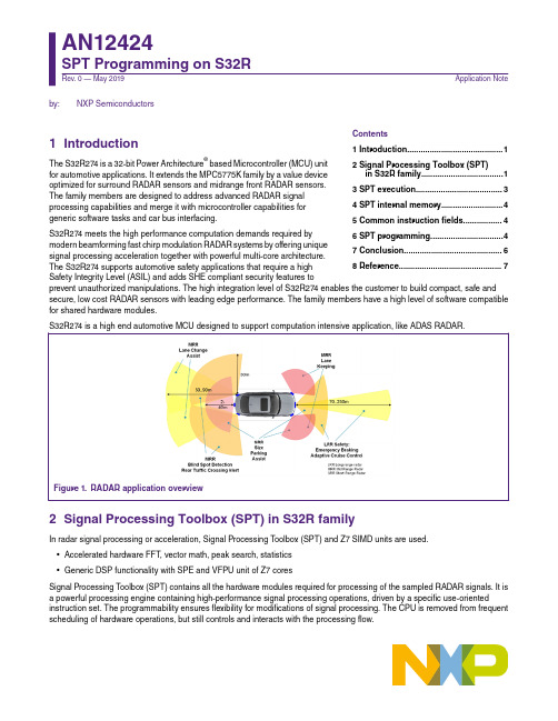
by:NXP Semiconductors1Introduction The S32R274 is a 32-bit Power Architecture ® based Microcontroller (MCU) unitfor automotive applications. It extends the MPC5775K family by a value deviceoptimized for surround RADAR sensors and midrange front RADAR sensors.The family members are designed to address advanced RADAR signalprocessing capabilities and merge it with microcontroller capabilities forgeneric software tasks and car bus interfacing.S32R274 meets the high performance computation demands required by modern beamforming fast chirp modulation RADAR systems by offering unique signal processing acceleration together with powerful multi-core architecture.The S32R274 supports automotive safety applications that require a highSafety Integrity Level (ASIL) and adds SHE compliant security features toprevent unauthorized manipulations. The high integration level of S32R274 enables the customer to build compact, safe and secure, low cost RADAR sensors with leading edge performance. The family members have a high level of software compatible for shared hardware modules.S32R274 is a high end automotive MCU designed to support computation intensive application, like ADAS RADAR.Figure 1.RADAR application overview2Signal Processing Toolbox (SPT) in S32R familyIn radar signal processing or acceleration, Signal Processing T oolbox (SPT) and Z7 SIMD units are used.•Accelerated hardware FFT , vector math, peak search, statistics•Generic DSP functionality with SPE and VFPU unit of Z7 coresSignal Processing T oolbox (SPT) contains all the hardware modules required for processing of the sampled RADAR signals. It is a powerful processing engine containing high-performance signal processing operations, driven by a specific use-orientedinstruction set. The programmability ensures flexibility for modifications of signal processing. The CPU is removed from frequent scheduling of hardware operations, but still controls and interacts with the processing flow.Contents1 Introduction (1)2 Signal Processing Toolbox (SPT)in S32R family....................................13 SPT execution......................................34 SPT internal memory...........................45 Common instruction fields.................46 SPT programming................................47 Conclusion. (6)8 Reference.............................................7AN12424SPT Programming on S32R Rev. 0 — May 2019Application NoteSPT is connected to the device by an advanced high performance master bus and a peripheral bus.Figure 2.SPT in S32R274 block diagramThe system bus master interface performs fast data transfers between external memory and local RAM.The purpose of the peripheral interface is to set configuration, get status information and basic control of SPT (start/stop, program pointer) and to trigger interrupts. It can also be used to exchange small amounts of the data between the CPU and the SPT , such as constant operands.Figure 3.SPT block diagramIt has the following features:•Acquisition of ADC samples—Capturing of ADC samples within programmed window—On-the-fly statistical computation—Supports MIPICSI2 interface•Provides HW acceleration for—FFT (8 - 4096 point)—Histogram calculation—Maximum and peak searchSignal Processing Toolbox (SPT) in S32R family—Mathematical operations on vector data•High-speed DMA data transfer—Supports system RAM, TCM and Flash memory transfers—Includes compression/decompression capability for reduction of storage footprint•Instruction based program flow—High-level commands for signal processing operations—Simple control commands—Local instruction buffer—Automatic instruction fetch from main memory—CPU interaction possible•CPU interruption notification•Watchdog•Debug Support - Single Stepping and Jamming ModeIt has three operation modes:1.STOP mode2.System Debug mode3.Normal mode3SPT executionThe SPT executes a list of instructions. These commands contain all the information to perform signal processing operations on data vectors consisting of a set of numbers. The instruction list is provided by the CPU in a memory buffer (SRAM or flash) and read by the SPT with autonomous triggered DMA operations. Preparation of command scripts is performed off-line duringdevelopment on a different system, such as a PC.Figure 4.SPT operation modelData as results or inputs of signal processing operations can be transferred between operand/twiddle RAM and system RAM or TCM by DMA operations. These kind of DMA operations are also scheduled by commands in the script.CPU application software functions may be invoked between signal processing operations. In order to synchronize these SW functions with the processing flow, interrupts and polling flags are provided, which may be activated as a result of specificcommands. In the same way, eDMA operations can be triggered from the SPT . The data transfer descriptors need to be prepared by application software.T o enable advanced and precisely timed pipelining of HW assisted operations, SPT command execution can also be synchronized with or triggered by events from CTE or MIPICSI2.SPT executionSPT internal memoryProgram execution is performed by a dedicated register machine. The program execution may be stalled at the end of each command and can be synchronized with events provided by the CTE or MIPICSI2. The CPU can stop and release program execution and execute its own instructions in the same time.The SPT command sequence is provided by CPU SW and written to a buffer in the system RAM or flash, where CSDMA fetches or alternatively transfers the list of instructions to the command queue.The program is executed sequentially, one command following the next in the chain with the exception being loops and asynchronous PDMA instruction. The end of a sequence is marked with a specific termination command. The start address of the instruction sequence is configured by application software using the peripheral interface.The command queue stores a number of instructions to be executed, which may be a shorter sequence than the complete instruction list. It maintains an instruction pointer to the current executed operation, which is incremented when the current operation is completed. This instruction pointer indicates the position in the complete instruction list sequence relative to the first instruction.Loop instructions are special cases, the program sequence may continue with a lower address depending on the state of the loop counter. The start and next command address of the loops are saved in special registers. Up to four nested loops are supported. Jump instructions or branch instructions are another case where the program may cause the program to branch to a non-contiguous address location. It is the responsibility of the assembler to ensure that the sanity of the program structure is not violated i.e. infinite loops, jumping into or out of a loop, etc.4SPT internal memorySPT contains internal memory resources namely, Operand RAM, Twiddle RAM and work registers. Out of these, only the work registers can be directly accessed via the peripheral interface and are visible on the SPT external memory map.The CPU can access these internal memory resources via the hardware accelerators. The instruction bitfields SRC_ADD and DEST_ADD point to these memories.The Twiddle RAM extends from location 0x4000 to 0x4FFF. However the area from 0x5000 to 0x7FFF is aliased to the Twiddle RAM i.e. it wraps around to point to the T widdle RAM. It should be noted that the memory accesses to the T widdle RAM should not cross the area from 0x4000 to 0x7FFF.The Operand RAM extends from location 0x8000 to 0xBFFF. But the area from 0xC000 to 0xFFFF is aliased to the Operand RAM. The memory accesses to the Operand RAM should not cross the area from 0x8000 to 0xFFFF.5Common instruction fieldsCommon instructions contains the following fields.•Opcode•Source and Destination address•Indirect Memory address•Source and destination address increment•Vector size•Input datatype/preprocessing6SPT programming6.1Programming based on RSDKNXP Radar SDK(RSDK) provides basic radar processing algorithms and device drivers for S32R hardware devices. Its purpose is to facilitate radar algorithm development (using SPT kernels, MA TLAB models), creation of higher level algorithms (starting from the basic blocks supplied with RSDK) and easy application development by integrating driver and platform support.Radar SDK (Radar SDK for S32R27 SPT accelerator ) could be downloaded from NXP website.RSDK SPT module consists of the SPT Driver, SPT Kernels software components.The SPT Driver serves as an interface between the user application running on the host CPU cores and the SPT hardware. The figure below shows a high-level block diagram of SPT software architecture. Its purpose is to enable the integration and executionof low-level microcode kernels on the SPT (Signal Processing T oolbox) accelerator for baseband radar signal processing.Figure 5.SPT software architectureThe SPT Kernels are individual precompiled routines of SPT code packed into a library, each implementing a part of the radar processing flow.T ogether, the SPT Driver and SPT Kernels library provide a software abstraction of the built-in SPT hardware functions (e.g. FFT ,Maximum Search, Histogram etc.) combined in a series of algorithms.The RSDK package also includes RSDK Sample Applications showing how to integrate these software components into the user code.6.2Programming based on graphic toolS32 Design Studio SPT graphical tool allows user to use graphical modeling workbench by leveraging the Eclipse Modeling technologies. It provides a workbench for model-based architecture engineering. Graphical tool equips teams who have to deal with complex architectures. The graphical tool includes everything necessary to easily create and manipulate models. The output of this tool is SPT assembler source code.The SPT graphical tool is integrated with the New S32DS Project wizard for devices which have SPT module. SPT1, SPT2 and SPT2.5 versions of SPT modules are supported. The SPT graphical tool can be used after project creation with the new graph tools project wizard. For detailed description of new project wizards, please read S32 Design Studio for Power Architecture, Version 2017.R1 reference manual.After the project is generated, SPT graphical tool windows could be gotten in IDE. User could drag 'Instructions', 'Flow' and 'Directives' from Palette window into working flow window.SPT programmingEach 'Instructions', 'Flow' or 'Directives' could change their setting in properties window. After finished the design of SPT working flow, generate SPT code through right click mouse.Figure 6.Generate project with SPT graphical toolFigure 7.SPT graphical tool windowsFigure 8.Example working flow and generate code7ConclusionThe SPT is a powerful processing engine containing high-performance signal processing operations driven by a specific instruction set. Its programmability ensures flexibility while removing the CPU from frequent scheduling of hardware operations, while still controlling and interacting with the processing flow. RSDK supports the API of SPT for customer and graphics tool for SPT programming could meet the flexible design request.8Reference•S32R274 Reference Manual•Radar SDK for S32R27 SPT accelerator •AN5375, S32R RADAR Signal CompressionHow To Reach Us Home Page: Web Support: /support Information in this document is provided solely to enable system and software implementers to use NXP products. There are no express or implied copyright licenses granted hereunder to design or fabricate any integrated circuits based on the information in this document. NXP reserves the right to make changes without further notice to any products herein.NXP makes no warranty, representation, or guarantee regarding the suitability of its products for any particular purpose, nor does NXP assume any liability arising out of the application or use of any product or circuit, and specifically disclaims any and all liability, including without limitation consequential or incidental damages. “Typical” parameters that may be provided in NXP data sheets and/or specifications can and do vary in different applications, and actual performance may vary over time. All operating parameters, including “typicals,” must be validated for each customer application by customer's technical experts. NXP does not convey any license under its patent rights nor the rights of others. NXP sells products pursuant to standard terms and conditions of sale, which can be found at the following address: / SalesTermsandConditions.While NXP has implemented advanced security features, all products may be subject to unidentified vulnerabilities. Customers are responsible for the design and operation of their applications and products to reduce the effect of these vulnerabilities on customer’s applications and products, and NXP accepts no liability for any vulnerability that is discovered. Customers should implement appropriate design and operating safeguards to minimize the risks associated with their applications and products.NXP, the NXP logo, NXP SECURE CONNECTIONS FOR A SMARTER WORLD, COOLFLUX, EMBRACE, GREENCHIP, HIT AG, I2C BUS, ICODE, JCOP, LIFE VIBES, MIFARE, MIFARE CLASSIC, MIFARE DESFire, MIFARE PLUS, MIFARE FLEX, MANTIS, MIFARE ULTRALIGHT, MIFARE4MOBILE, MIGLO, NTAG, ROADLINK, SMARTLX, SMARTMX, ST ARPLUG, TOPFET, TRENCHMOS, UCODE, Freescale, the Freescale logo, AltiVec, C‑5, CodeTEST, CodeWarrior, ColdFire, ColdFire+, C‑Ware, the Energy Efficient Solutions logo, Kinetis, Layerscape, MagniV, mobileGT, PEG, PowerQUICC, Processor Expert, QorIQ, QorIQ Qonverge, Ready Play, SafeAssure, the SafeAssure logo, StarCore, Symphony, VortiQa, Vybrid, Airfast, BeeKit, BeeStack, CoreNet, Flexis, MXC, Platform in a Package, QUICC Engine, SMARTMOS, Tower, TurboLink, and UMEMS are trademarks of NXP B.V. All other product or service names are the property of their respective owners. AMBA, Arm, Arm7, Arm7TDMI, Arm9, Arm11, Artisan, big.LITTLE, Cordio, CoreLink, CoreSight, Cortex, DesignStart, DynamIQ, Jazelle, Keil, Mali, Mbed, Mbed Enabled, NEON, POP, RealView, SecurCore, Socrates, Thumb, TrustZone, ULINK, ULINK2, ULINK-ME, ULINK-PLUS, ULINKpro, µVision, Versatile are trademarks or registered trademarks of Arm Limited (or its subsidiaries) in the US and/or elsewhere. The related technology may be protected by any or all of patents, copyrights, designs and trade secrets. All rights reserved. Oracle and Java are registered trademarks of Oracle and/or its affiliates. The Power Architecture and word marks and the Power and logos and related marks are trademarks and service marks licensed by .© NXP B.V. 2019.All rights reserved.For more information, please visit: Forsalesofficeaddresses,pleasesendanemailto:**********************Date of release: May 2019Document identifier: AN12424。

三维立体阵列波束赋形Three-dimensional beamforming in an array is atechnique used to enhance the performance of wireless communication systems. It involves shaping the radiation pattern of an antenna array in order to focus thetransmitted or received signal towards a specific direction. This technology has gained significant attention in recent years due to its potential to improve the capacity, coverage, and reliability of wireless networks.One of the main advantages of three-dimensional beamforming is its ability to mitigate interference. By focusing the transmitted signal in a specific direction, it is possible to reduce the interference caused by signals coming from other directions. This can significantlyimprove the signal quality and increase the capacity of the wireless network. In addition, three-dimensional beamforming can also be used to null out interference from specific directions, further improving the overall system performance.Another important aspect of three-dimensional beamforming is its ability to improve the coverage of wireless networks. By shaping the radiation pattern of the antenna array, it is possible to increase the signal strength in specific areas, extending the coverage of the network. This is particularly useful in environments with challenging propagation conditions, such as urban areas with high-rise buildings or rural areas with limited infrastructure.Furthermore, three-dimensional beamforming can also be used to improve the reliability of wireless communication systems. By focusing the transmitted signal towards the intended receiver, it is possible to increase the signal-to-noise ratio, reducing the impact of noise and interference. This can result in a more reliable and stable wireless connection, especially in scenarios with high interference levels or fading channels.In addition to its technical advantages, three-dimensional beamforming also has the potential to enablenew applications and services. For example, it can be used to provide targeted coverage in specific areas, such as stadiums or shopping malls, where high-capacity andreliable wireless connectivity is required. It can also be used to support emerging technologies, such as virtual reality or augmented reality, which demand high data rates and low latency.Despite its potential benefits, there are also challenges associated with three-dimensional beamforming. One of the main challenges is the complexity of the algorithms and hardware required to implement this technology. Three-dimensional beamforming requires precise control of the phase and amplitude of the signals transmitted by each antenna element in the array. This requires sophisticated signal processing algorithms and high-performance hardware, which can be costly anddifficult to implement in practice.Another challenge is the limited scalability of three-dimensional beamforming. As the number of antennas in the array increases, the complexity and cost of the system alsoincrease. This makes it challenging to deploy large-scale three-dimensional beamforming systems in practical scenarios. Additionally, the performance of three-dimensional beamforming is highly dependent on the accuracy of the channel state information, which can be difficult to estimate accurately in real-world environments.In conclusion, three-dimensional beamforming in an array is a promising technology that can significantly improve the performance of wireless communication systems. It offers advantages such as interference mitigation, improved coverage, and enhanced reliability. However, there are challenges associated with its implementation,including algorithm complexity, hardware requirements, and scalability issues. Despite these challenges, three-dimensional beamforming has the potential to enable new applications and services and drive the evolution of wireless networks towards higher capacity and improved quality of service.。

数字超表面国内研究数字超表面(Digital Metasurface)是一种能够对电磁波进行精确调控的新型材料,近年来在国内得到了广泛的研究关注。
本文将介绍数字超表面的基本原理、国内的研究进展以及未来的发展方向。
数字超表面是一种由二维阵列结构构成的人工表面,每一个单元格都包含了一个微小的天线和一个可编程的电路。
通过控制每个单元格的相位和振幅,数字超表面可以实现对电磁波的精确调控,包括波束操控、相位调制、极化转换等功能。
与传统的天线技术相比,数字超表面具有体积小、重量轻、功耗低等优点,可以在通信、雷达、成像等领域发挥重要作用。
在国内,数字超表面的研究起步较晚,但近年来取得了快速的发展。
首先,国内的研究团队在数字超表面的设计和制备方面取得了重要的突破。
他们利用微纳加工技术制备出了具有高精度的数字超表面结构,并通过优化设计算法实现了对电磁波的高效调控。
国内的研究团队在数字超表面的应用方向上也进行了广泛的探索。
他们将数字超表面应用于通信系统中,实现了对无线信号的波束操控,提高了信号传输的可靠性和效率。
同时,数字超表面还可以用于雷达系统中,通过对电磁波的相位调制,实现了对目标的高分辨成像。
此外,数字超表面还可以用于光学系统中,实现对光波的聚焦和偏振转换,有望在光通信和光计算领域发挥重要作用。
未来,数字超表面在国内的研究方向有望进一步扩展。
首先,研究人员可以进一步优化数字超表面的设计和制备技术,提高其调控性能和稳定性。
其次,可以将数字超表面与其他新型材料相结合,实现更多种类的功能。
例如,将数字超表面与拓扑绝缘体相结合,可以实现对电磁波的拓扑调控;将数字超表面与光子晶体相结合,可以实现对光波的超透镜效应。
此外,还可以探索数字超表面在声波和机械波领域的应用,拓宽其应用范围。
数字超表面是一种具有重要应用前景的新型材料,在国内得到了广泛的研究关注。
国内的研究团队在数字超表面的设计、制备和应用方向上取得了重要进展,并展望了未来的发展方向。

One Technology Way · P.O. Box 9106 · Norwood, MA 02062-9106 · Tel: 781.329.4700 · Fax: 781.461.3113 · EVALUATING THE AD9653/AD9253/AD9633 ANALOG-TO-DIGITAL CONVERTERSPrefaceThis user guide describes the AD9653, AD9253 and AD9633 evaluation boards, AD9653-125EBZ,AD9253-125EBZ and AD9633-125EBZ, which provide all of the support circuitry required to operate these parts in their various modes and configurations. The application software used to interface with the devices is also described.The AD9653AD9253 and AD9633 data sheets provide additional information and should be consulted when using the evaluation board. All documents and software tools are available at/hsadcevalboard. For additional information or questions, send an email to*******************************.Typical Measurement SetupFigure 1. Evaluation Board Connection—AD9653-125EBZ, AD9253-125EBZ or AD9633-125EBZ (on Left)and HSC-ADC-EVALCZ (on Right)FeaturesFull featured evaluation board for the AD9653/AD9253/AD9633qSPI interface for setup and controlqExternal, on-board oscillator, or AD9517 clocking optionqBalun/transformer or amplifier input drive optionqOn-board LDO regulator needing a single external 6 V, 2 A dc supplyqVisualAnalog® and SPI controller software interfacesqHelpful DocumentsAD9653, AD9253 or AD9633 data sheetqHigh speed ADC FIFO evaluation kit (HSC-ADC-EVALCZ)qAN-905 Application Note, VisualAnalog Converter Evaluation Tool Version 1.0 User ManualqAN-878 Application Note, High Speed ADC SPI Control SoftwareqAN-877 Application Note, Interfacing to High Speed ADCs via SPIqAN-835 Application Note, Understanding ADC Testing and EvaluationqDesign and Integration FilesSchematics, layout files, bill of materialsqEquipment NeededAnalog signal source and antialiasing filterqSample clock source (if not using the on-board oscillator)q2 switching power supplies (6.0 V, 2.5 A), CUI EPS060250UH-PHP-SZ providedqPC running Windows®qUSB 2.0 portqAD9653-125EBZ, AD9253-125EBZ or AD9633-125EBZ boardqHSC-ADC-EVALCZ FPGA-based data capture kitqGetting StartedThis section provides quick start procedures for using the AD9653-125EBZ, AD9253-125EBZ or AD9633-125EBZ board. Both the default and optional settings are described.Configuring the BoardBefore using the software for testing, configure the evaluation board as follows:1.Connect the evaluation board to the data capture board, as shown in Figure 1.2.Connect one 6 V, 2.5 A switching power supply (such as the CUI, Inc., EPS060250UH-PHP-SZ that is supplied) to the AD9653-125EBZ, AD9253-125EBZ or AD9633-125EBZ.3.Connect one 6 V, 2.5 A switching power supply (such as the supplied CUI EPS060250UH-PHP-SZ) to the HSC-ADC-EVALCZ board.Connect the HSC-ADC-EVALCZ board (J6) to the PC using a USB cable.4.5.On the ADC evaluation board, confirm that the jumpers are installed as shown in Figure 2 and Table 1.On the ADC evaluation board, use a clean signal generator with low phase noise to provide an6.input signal to the desired A and/or B channel(s). Use a 1 m, shielded, RG-58, 50 Ω coaxial cable to connect the signal generator. For best results, use a narrow-band, band-pass filter with 50 Ωterminations and an appropriate center frequency. (Analog Devices, Inc., uses TTE, Allen Avionics, and K&L band-pass filters.)Evaluation Board HardwareThe evaluation board provides the support circuitry required to operate the AD9653, AD9253 andAD9633 in their various modes and configurations. Figure 1 shows the typical bench characterization setup used to evaluate AC performance. It is critical that the signal sources used for the analog input and clock have very low phase noise (<1 ps rms jitter) to realize the optimum performance of the signal chain. Proper filtering of the analog input signal to remove harmonics and lower the integrated or broadband noise at the input is necessary to achieve the specified noise performance.See the Getting Started section to get started, and visit UG-328 Design Support for the complete schematics and layout diagrams. These diagrams demonstrate the routing and grounding techniques that should be applied at the system level when designing application boards using these converters.Power SuppliesThis evaluation board comes with a wall-mountable switching power supply that provides a 6 V, 2 A maximum output. Connect the supply to a 100 V ac to 240 V ac, 47 Hz to 63 Hz wall outlet. The output from the supply is provided through a 2.1 mm inner diameter jack that connects to the printed circuit board (PCB) at P101. The 6 V supply is fused and conditioned on the PCB before connecting to the low dropout linear regulators that supply the proper bias to each of the various sections on the board.The evaluation board can be powered in a nondefault condition using external bench power supplies. To do this, remove the E101, E102, E103 and E104 ferrite beads to disconnect the outputs from theon-board LDOs. This enables the user to bias each section of the board individually. Use P102 andP103 to connect a different supply for each section. A 1.8 V, 0.5 A supply is needed for 1.8V_AVDD and 1.8V_DRVDD. Although the power supply requirements are the same for AVDD and DRVDD, it is recommended that separate supplies be used for both analog and digital domains. The SPI and its level shifters and alternate clock options require a separate 3.3 V, 0.5 A analog supply.Two additional supplies, 5V_AVDD and 3V_AVDD, are used to bias the optional input path amplifiers and optional AD9517-3 clock chip. If used, these supplies should each have 0.5 A current capability. Input SignalsWhen connecting the ADC clock and analog source, use clean signal generators with low phase noise, such as the Rohde & Schwarz SMA, or HP 8644B signal generators or an equivalent. Use a 1 m shielded, RG-58, 50 Ω coaxial cable for connecting to the evaluation board. Enter the desired frequency and amplitude (see the Specifications section in the data sheet of the respective part). When connecting the analog input source, use of a multipole, narrow-band band-pass filter with 50 Ωterminations is recommended. Analog Devices uses band-pass filters from TTE and K&L Microwave, Inc. Connect the filters directly to the evaluation board.If an external clock source is used, it should also be supplied with a clean signal generator as previously specified. Analog Devices evaluation boards typically can accept ~2.8 V p-p or 13 dBm sine wave input for the clock.Output SignalsThe default setup uses the Analog Devices high speed converter evaluation platform (HSC-ADC-EVALCZ) for data capture. The serial LVDS outputs from the ADC are routed to ConnectorP1002 using 100 Ω differential traces. For more information on the data capture board and its optional settings, visit /hsadcevalboard.Jumper SettingsSet the jumper settings/link options on the evaluation board for the required operating modes before powering on the board. The functions of the jumpers are described in Table 1. Figure 2 shows the default jumper settings.Table 1. Jumper SettingsJumperDescriptionJ202This jumper selects between internal V REF and external V REF .To choose the internal 1 V reference, connect Pin 3 (DUT_SENSE) to Pin 5 (GND).To use the on-board ADR130 1 V reference, connect Pin 2 (DUT_SENSE) to Pin 1 (AVDD), and connect Pin 4 (DUT_VREF) to Pin 6 (EXT_REF).To apply a reference voltage from an external off-board source, connect Pin 2 (DUT_SENSE)to Pin 1 (AVDD) and apply the reference voltage to Pin 4 (DUT_VREF). The AD9653 canaccommodate reference voltages from 1.0 V to 1.3 V; the AD9253 and AD9633 referencevoltage is specified to be 1.0 V.J204Use this jumper to power down the ADC. Using the SPI, the PDWN pin can be configured to be STBY (standby).J302This jumper sets the ADC for SPI communications with the HSC-ADC-EVALCZ .Connect Pin 1 to Pin 2 for SDIO, Pin 4 to Pin 5 for SCLK, and Pin 8 to Pin 9 for CSB.J803This jumper enables the on-board crystal oscillator.Figure 2. Default Jumper Connections for AD9653-125EBZ /AD9253-125EBZ /AD9633-125EBZ Board Evaluation Board CircuitryThis section explains the default and optional settings or modes allowed on the AD9653-125EBZ ,AD9253-125EBZ and the AD9633-125EBZ boards.PowerPlug the switching power supply into a wall outlet rated at 100 V ac to 240 V ac, 47 Hz to 63 Hz. Connect the DC output connector to P101 on the evaluation board.Analog InputThe four channel inputs on the evaluation board are set up for a double balun-coupled analog input with a 50 Ω impedance. The default analog input configuration supports analog input frequencies of up to ~200 MHz.VREFThe default VREF configuration is to connect the SENSE pin to AGND for internal VREF operation. This is done by connecting Pin 3 to Pin 5 on Header J202. An external reference voltage can be provided to the AD9653, AD9253 and AD9633. Connecting Pin 2 to Pin 1 on Header J202 puts the ADC in a mode where it requires a reference voltage from an external source. The external on-board 1.0 V reference is provided by the ADR130. This external reference can be connected to the ADC by connecting Pin 4 to Pin 6 on Header J202. Alternatively, if an external off-board reference is desired, connect Pin 2 to Pin1 on Header J202 and apply the reference voltage directly to Pin 4 of Header J202. The AD9653 can accommodate reference voltages from 1.0 V to 1.3 V; the AD9253 and AD9633 reference voltage is specified to be 1.0 V.RBIASRBIAS has a default setting of 10 kΩ (R205) to ground and is used to set the ADC core bias current. Note that using a resistor value other than a 10 kΩ, 1% resistor for RBIAS may degrade the performance of the device.ClockThe default clock input circuit is derived from a simple transformer-coupled circuit using a high bandwidth 1:1 impedance ratio transformer (T801/T802) that adds a low amount of jitter to the clock path. The clock input is 50 Ω terminated and ac-coupled to handle single-ended sine wave types of inputs. The transformer converts the single-ended input to a differential signal that is clipped byCR801 before entering the ADC clock inputs. The AD9653, AD9253 and AD9633 ADCs are equipped with an internal 8:1 clock divider to facilitate usage with higher frequency clocks. When using the internal divider and a higher input clock frequency, remove CR801 to preserve the slew rate of the clock signal.The AD9653-125EBZ, AD9253-125EBZ and AD9633-125EBZ boards are set up to be clocked through the transformer-coupled input network from the crystal oscillator, Y801. This oscillator is a low phase noise oscillator from Valpey Fisher (VFAC3-BHL-125MHz). If a different clock source is desired, remove C810 (optional) and Jumper J803 to disable the oscillator from running and connect the external clock source to the SMA connector, J802 (labeled CLK+).PDWNTo enable the power-down feature, add a shorting jumper across J204 at Pin 1 and Pin 2 to connect the PDWN pin to DRVDD.Modes of OperationStandalone (PIN) ModeThe AD9653/AD9253/AD9633 ADCs can operate in pin mode if there is no need to program and change the default modes of operation via the SPI. For applications that do not require SPI mode operation, the CSB pin is tied to AVDD, and the SDIO/OLM pin controls the output lane mode. Table 2 and Table 3 specify the settings for pin mode operation.Table 2. Output Lane Mode (OLM) Pin SettingsOLM Pin Voltage Output ModeAVDD (Default)Two-lane. 1× frame, 16-bit serial outputGND One-lane. 1× frame, 16-bit serial outputTable 3. Digital Test Pattern (DTP) Pin SettingsSeected DTP Output Mode Resulting D0±x and D1±xNormal Operation10 kΩ to AGND Normal operationDTP AVDD1000 0000 0000 0000Additional information on the lane modes is provided in the AD9653, AD9253 and AD9633 data sheets.Default ModeTo operate the device under test (DUT) using the SPI, follow the jumper settings for J302 as shown in Table 1.How To Use The Software For TestingSetting up the ADC Data CaptureAfter configuring the board, set up the ADC data capture using the following steps:1.Open VisualAnalog on the connected PC. The appropriate part type should be listed in the status bar of the VisualAnalog – New Canvas window. Select the template that corresponds to the type of testing to be performed (see Figure 3, where the AD9253 is shown as an example).Figure 3. VisualAnalog, New Canvas Window2.After the template is selected, a message appears asking if the default configuration can be used to program the FPGA (see Figure 4). Click Yes, and the window closes.Figure 4. VisualAnalog Default Configuration Message3.To change features to settings other than the default settings, click the Expand Display button,located on the bottom right corner of the window (see Figure 5), to see what is shown in Figure 6. 4.Change the features and capture settings by consulting the detailed instructions in the AN-905 Application Note, VisualAnalog Converter Evaluation Tool Version 1.0 User Manual. After the changes are made to the capture settings, click the Collapse Display button.Figure 5. VisualAnalog Window Toolbar, Collapsed DisplayFigure 6. VisualAnalog, Main Window Expanded DisplayEvaluation And TestSetting up the SPI Controller SoftwareAfter the ADC data capture board setup is complete, set up the SPI controller software using the following procedure:1.Open the SPI controller software by going to the Start menu or by double-clicking theSPIController software desktop icon. If prompted for a configuration file, select the appropriate one. If not, check the title bar of the window to determine which configuration is loaded. Ifnecessary, choose Cfg Open from the File menu and select the appropriate file based on your part type. Note that the CHIP ID(1) box should be filled to indicate whether the correct SPI controller configuration file is loaded (see Figure 7).Figure 7. SPI Controller, CHIP ID(1) BoxClick the New DUT button in the SPIController window (see Figure 8)2.Figure 8. SPI Controller, New DUT Button3.In the ADCBase 0 tab of the SPIController window, find the CLOCK DIVIDE(B) box (see Figure9). If using the clock divider, use the drop-down box to select the correct clock divide ratio, ifnecessary. For additional information, refer to the data sheet, the AN-878 Application Note, High Speed ADC SPI Control Software, and the AN-877 Application Note, Interfacing to High Speed ADCsvia SPI.Figure 9. SPI Controller, CLOCK DIVIDE(B) Box4.Note that other settings can be changed on the ADCBase 0 tab (see Figure 9) and the ADC A, ADC B, ADC C, and ADC D tabs (see Figure 10) to set up the part in the desired mode. TheADCBase 0 tab settings affect the entire part, whereas the settings on the ADC A, ADC B, ADC C, and ADC D tabs affect the selected channel only. See the appropriate part data sheet, the AN-878 Application Note, High Speed ADC SPI Control Software, and the AN-877 Application Note,Interfacing to High Speed ADCs via SPI, for additional information on the available settings.Figure 10. SPI Controller, Example ADC A Page5.Click the Run button in the VisualAnalog toolbar (see Figure 11).Figure 11. Run Button (Encircled in Red) in VisualAnalog Toolbar, Collapsed DisplayAdjusting the Amplitude of the Input SignalThe next step is to adjust the amplitude of the input signal for each channel as follows:Adjust the amplitude of the input signal so that the fundamental is at the desired level. Examine 1.the Fund Power reading in the left panel of the VisualAnalog Graph - AD9253 FFT window(see Figure 12).Figure 12. Graph Window of VisualAnalogRepeat this procedure for Channel B, Channel C, and Channel D.2.3.Click the disk icon within the VisualAnalog Graph - AD9253 FFT window to save theperformance plot data as a .csv formatted file. See Figure 13 for an example.Figure 13. Typical FFT, AD9253Troubleshooting TipsIf the FFT plot appears abnormal, do the following:If you see an abnormal noise floor, go to the ADCBase0 tab of the SPIController window andqtoggle the Chip Power Mode in MODES(8) from Chip Run to Reset and back.If you see a normal noise floor when you disconnect the signal generator from the analog input, be qsure that you are not overdriving the ADC. Reduce the input level if necessary.In VisualAnalog, click the Settings icon in the Input Formatter block. Check that NumberqFormat is set to the correct encoding (twos complement by default). Repeat for the other channels.If the FFT appears normal but the performance is poor, check the following:Make sure that an appropriate filter is used on the analog input.qMake sure that the signal generators for the clock and the analog input are clean (low phase noise). qChange the analog input frequency slightly if noncoherent sampling is being used.qMake sure that the SPI configuration file matches the product being evaluated.qIf the FFT window remains blank after Run in VisualAnalog (see Figure 11) is clicked, do the following:Make sure that the evaluation board is securely connected to the HSC-ADC-EVALCZ board.qMake sure that the FPGA has been programmed by verifying that the DONE LED is illuminated onqthe HSC-ADC-EVALCZ board. If this LED is not illuminated, make sure that the U4 switch on the board is in the correct position for USB CONFIG.Make sure that the correct FPGA program was installed by clicking the Settings icon in the ADCqData Capture block in VisualAnalog. Then select the FPGA tab and verify that the proper FPGA bin file is selected for the part.If VisualAnalog indicates that the FIFO Capture timed out, do the following:Make sure that all power and USB connections are secure.qProbe the DCO signal at P1002 (Pin A10 and/or Pin B10) on the evaluation board, and confirm that a qclock signal is present at the ADC sampling rate.© Analog Devices, Inc. All rights reserved. Trademarks andregistered trademarks are the property of their respective 。
Extraction of Virtual Scattering Centers of Vehicles by Ray-Tracing SimulationsKarin Schuler,Denis Becker,and Werner Wiesbeck,Fellow,IEEEAbstract—Radar images of complex targets can be understood as a superposition of the reflected signals from a high number of scattering centers.To model complex targets for radar simulations, the plurality of scattering centers should be reduced to few signifi-cant scattering centers in order to minimize computational effort. The scope of this work is to present a technique to generate a signif-icantly simplified RCS model of the vehicle with a limited number of virtual scattering centers,each with its own scattering charac-teristic,and how to group these scattering centers in a cluster data-base.The work is based on ray-tracing simulations of complex vehicle models.The ray-tracing simulations have been validated by measurements.The scattering centers may not be physically existing strong scattering centers,but virtual scattering centers representing a certain scattering behavior.In this paper,a tech-nique for extracting such virtual scattering centers from a complex 3D-vehicle-model is presented.It is based on ray-tracing simula-tions of such models.As an example,the design model of a Ford Focus is used.Index Terms—Ray-tracing,RCS-modeling,scattering center.I.I NTRODUCTIOND URING the last years,safety relevant sensor systems havebecome an important feature in the automotive industry. Presently,short range radar(SRR)systems are being devel-oped and introduced to the market.Their intention is to cover the near surrounding of a vehicle to assist the driver during Stop-n-Go traffic and parking,but also to increase safety by blind-spot surveillance and side impact warnings.Currently,dif-ferent approaches are being discussed for the realization of a radar sensor with full azimuth coverage and high azimuth res-olution of the close-by environment.To simulate and evaluate the performance of different approaches for such SRR-systems, scattering-models of vehicles are required.Since vehicles ob-served in the close-by region exhibit multiple scattering centers, contributions from different angles are expected.Depending on the incidence angle,they cause multiple intensity maxima in radar images[1].By describing the scattering characteristics of complex objects by one single RCS value,the multiple scat-tering centers and other scattering phenomena are not apparentManuscript received January22,2007;revised July12,2008.Current version published November14,2008.K.Schuler was with the Universität Karlsruhe(TH),Institut für Höch-stfrequenztechnik und Eletronik(IHE),Karlsruhe D76131,Germany.She is now with EADS Defence Electronics,Ulm D89077,Germany(e-mail: karin.schuler@a.de).D.Becker and W.Wiesbeck are with the Universität Karlsruhe(TH),Institut für Höchstfrequenztechnik und Eletronik(IHE),Karlsruhe D76131,Germany (e-mail:denis.becker@a.de;werner.wiesbeck@a.de).Color versions of one or more of thefigures in this paper are available at .Digital Object Identifier10.1109/TAP.2008.2005436anymore.For this reason,it is not sufficient to consider a single scattering center or an azimuth independent RCS in the simu-lations.However,the multiple scattering centers are important and have to be taken into account in radar imaging simulations with high azimuth resolution.A scattering center description for target recognition in one dimension is proposed in[2].Ap-proaches for scattering center extraction are suggested in[3], [4].There exist various numerical methods for the calculation of electromagneticfield distributions like the method of moments (MoM)[5],finite-difference-time-domain(FDTD)method[6] and thefinite element method(FEM).All these methods require a high discretization of the structure relative to the wavelength. At high frequencies,this leads to an immense computational ef-fort for large structures.Therefore,these numerical methods are not suited for large problems[7].In such cases,hybrid[8]or asymptotic methods based on geometrical optics(GO)or phys-ical optics(PO)are often used.Physical optics may also be ex-tended by physical theory of diffraction(PTD)[7],the method of equivalent currents(MEC)[9]and impedance boundary con-dition(IBC)techniques[10].These ray-tracing simulations deliver fast and reliable results when considering the scattering characteristic of complex ob-jects.However,sometimes even these simulations of complex models are too time-consuming.For electrically large problems like traffic scenarios,it is therefore crucial to derive a simplified scattering model,which delivers a good approximation for the scattering characteristic of the involved vehicles.In the following,a straightforward approach to generate such a simplified scattering model by determining the virtual scat-tering centers of the vehicle directly from ray-tracing simula-tions will be presented.In general,ray-tracing simulations determine the properties of the propagation paths between a transmitter and a receiver, including multiple non-line-of-sight paths.On the way from the transmitter to the receiver,the rays hit the simulation struc-ture at multiple points,which leads to reflection,diffraction and scattering.All these interaction points are called scattering cen-ters.The scattering centers are therewith a direct result of the ray-tracing simulation.The goal of this work is to group the scattering centers into so-called virtual scattering centers.The virtual scattering centers are representatives of the scattering be-havior of the structure itself and describe the most important ge-ometrical parts and their contributions to the scattering.The ray-tracing simulation results have been validated by measurements.Based on these results,a simplified scattering model is derived,consisting of multiple virtual scattering centers,each with its special scattering characteristic.These virtual scattering centers represent the simplified scattering0018-926X/$25.00©2008IEEEFig.1.Model of Ford Focus for IHE3D-ray-tracing.Fig.2.Coordinate system.model,which has a similar scattering behavior as the complex car model.This simplified scattering model allows the rapid investigation of a wide range of radar scattering situations,where a conventional ray-tracing method would be too complex or is not available.II.R AY -T RACING S IMULATIONSimulations of vehicles with commercial FDTD simulation tools are not feasible at frequencies of 24GHz or 76GHz,as they are specified for automotive radar applications.The dis-cretization of the model into sub-wavelength-elements would lead to too large matrices.Ray-tracing simulations do not suffer directly from this constraint.The crucial number for ray-tracing-simulations is the number of visible faces seen by the trans-mitter.This number is therewith rather related to the geometry’s complexity than to its size.RCS simulations with ray-tracing have also been presented in [7].One approach for the determination of scattering centers is presented in [11].In simulated ISAR images intensity maxi-mums are considered as scattering centers and subtracted from the radar image with the clean algorithm [12].The radar images are based on the shooting and bouncing ray technique and on the processing of ISAR images.This procedure therefore requires a detour when processing the ISAR image.A similar but frequency and aspect dependent technique for data compression of SAR and ISAR images is presented in [13].It is based on the extraction of point and line-segment scatterers from the measured radar image.In the following,the scattering information obtained by the ray-tracing simulation will be directly evaluated.The usedray-Fig.3.Example of bistatic ray-tracing simulation with IHE3D-ray-tracing.Fig.4.Bistatic measurements at JRC,Ispra,Italy,car outside the chamber.tracing tool has been developed at the Institut für Höchstfre-quenztechnik und Elektronik (IHE)at the University of Karl-sruhe (TH)in Germany.It is a ray optical approach for modeling wave propagation.Each ray is considered separately and takes into account multiple reflections,diffraction and scattering.This gives an insight to the scattering centers and the scattering phe-nomena that will be exploited in the following.Modified Fresnel coefficients are used to model rough surfaces.Diffraction is de-scribed by the uniform geometrical theory of diffraction (UTD)and the corresponding heuristic coefficients for wedge diffrac-tion.The ray-tracing tool has already been verified multiple times with measurements for various wave propagation simu-lations [14]–[17].The 3D-model of the car,which is considered in the fol-lowing,is illustrated in Fig.1.The model of the car consists of 12.100triangles.Each ofthem is at least25,guaranteeing a large area compared to the wavelengthat .This is important to fulfill the requirements of the ray-tracing tool.For calculating the reflections,the ray-tracing tool assumes rel-atively large areas and uses the modified Fresnel-coefficients for the calculation of the reflection coefficient.Therefore,the edgeSCHULER et al.:EXTRACTION OF VIRTUAL SCATTERING CENTERS OF VEHICLES3545Fig.5.Bistatic coupling coefficient for front illumination ('=180)in vertical polarization at f =24GHz .Left:measurement,right:simulation.Fig.6.Bistatic coupling coefficient at elevation angle =60for rear illumination ('=0).Left:vertical polarization,right:horizontal polarization.length of an element must be within 5to 10wavelength,which is fulfilled in this case.This condition determines also the max-imum number of elements.In this particular case of a vehicle,reflections are the majority of all interactions.If the number of elements is chosen significantly smaller,the ray-tracer will not find enough reflections to represent the scattering character-istic of the car precisely enough.This would also be the case for lower frequencies,for which the size of the triangles would have to be increased and therefore their number would become to small to give a precise representation of the cars geometry.For higher frequencies,more detailed models could be used,delivering even more accurate results.A material assignment is made for each discretization element of the car.It contains the parameters of the permittivity,the roughness and the loss.For the simulation,a ground floor was added to take multipath propagation effects also into account [18].III.V ERIFICATION OF R AY -T RACING S IMULATIONSThe bistatic scattering coefficient of a Ford Focus has been simulated with ray-tracing and compared to measurements of the same vehicle.In Fig.2the coordinate system and its origin is defined relative to the car.Fig.3shows the top view for a bistatic ray-tracing simulation.The lines indicate the propagation paths.The line-of-sight path is neglected.For each transmitter and receiver position,the dynamic range is limited to 100dB with reference to the strongest non-line-of-sight path.Up to five interactions as diffraction and reflection are considered per path.For scattering only one interaction is considered,since the power level of the scattered path is reduced drasti-cally.For each path,the path information is stored.The path information contains the number,types and locations of the interactions.Also the amplitude and the phase of the received signals are delivered.These parameters are obtained from the propagation time and the complex scattering coefficients of the interactions.The vehicle is illuminated from therearin the azimuthplane whereas the receiver performs a 360-turn along the azimuth.The simulations have been per-formed for both horizontal and vertical polarization.Similar simulations were performed for frontillumination .The same configurations are used in the verification measure-ments.The verification measurements were performed in the ane-choic chamber of the European Commission Joint Research Center (JRC),located at Ispra in northern Italy,and were pub-lished in [19].Fig.4shows the vehicle in front of the anechoic chamber.3546IEEE TRANSACTIONS ON ANTENNAS AND PROPAGATION,VOL.56,NO.11,NOVEMBER 2008With this setup,the bistatic coupling coefficient along the az-imuthangle and the elevationangle has been measured for the two cases:front and rear illumination,both in vertical and horizontal polarization.The coupling coefficient for front illu-mination has been simulated and measured along a spherical surface.It is plotted along the azimuthangle and the eleva-tionangle .In Fig.5the comparison between measurement and simulation is shown for vertical polarization.The transmitantenna was placed at azimuthangleand elevationangle .The receive antenna was moved along azimuthfromto and along elevationfromto in the upper hemisphere.Measurements have alreadybeen performed for the study presented in [19]with an angular step width of 5along azimuth and elevation.For the compar-ison between the measurement and the simulation,the bistatic simulations have been performed with the same step width.The comparisons show a good agreement for high elevationangles,which are close to the azimuth plane.The farther transmitter and receiver are positioned from each other,the more simulation and measurement differ from each other.However,the closer transmitter and receiver are positioned to each other,the better is the agreement.Since in the following only monostatic simulations will be analyzed,reliable results from these ray-tracing simulations are expected.For a closer look at the data,the coupling coefficient for aconstant elevationangleis shown in Fig.6.It shows the comparison of the simulated and the measured coupling co-efficient for rear illumination in vertical (left)and horizontal (right)polarization.For both polarizations,the coupling coef-ficient drops significantly when transmit and receive antennasareorientedrelative to each other.The agreement be-tween measurement and simulation is very good for azimuthanglebetweenand 160.For azimuth angles closeto ,the angle of reflection is relatively large.In this spe-cific configuration,the simulation leads to an increased reflec-tion coefficient since the coupling along the roof of the car is considered to strong.The here presented comparison uses a bistatic configuration due to the available measurements.It shows,that the closer transmit and receive antenna are situated to each other,the better is the agreement between simulation and measurement.This is important since the following simulations and the derivation of the virtual scattering model will be performed in monostatic configuration.This monostatic configuration can be looked at as the extreme case of a bistatic configuration,where both an-tennas are placed at the same location.However,the accuracy of the virtual scattering center model can not be higher than the accuracy of the initial ray-tracing simulation.This comparison proves the reliability of the ray-tracing simulations with this de-tailed simulation model of the Ford Focus.Therefore the anal-ysis of ray-tracing specific information like the location of scat-tering centers and the path information can be used for further analysis.IV .M ONOSTATIC V IRTUAL S CATTERING C ENTER E XTRACTION In the following,monostatic ray-tracing simulations in az-imuth will be evaluated.The analysis of the scatteringcentersFig.7.Scattering centers for monostatic simulation of FordFocus.Fig.8.Flowchart of implemented greedy-algorithm.leads to scattering clusters.To each cluster,a single virtual scat-tering center with its own scattering characteristic is assigned.The scattering characteristic is obtained by summarizing the scattering effects of all scattering centers belonging to one cluster.Of course,a high number of clusters will lead to a more precise model,but on the other hand,a model containing a low number of clusters will result in a faster calculation.It will be shown that it is possible to reduce the complex vehicle model to a limited number of clusters for characterizing the scattering behavior in the azimuth plane without compromising on the precision of the simulation.A.Simulation of Scattering CentersA monostatic simulation of the reflection coefficient has been performed along azimuth using 1step width along a circle withtheradius.Regarding the possible application of this model for Short Range Radar simulations,the angular resolution width is a good compromise between computation time and ac-curacy.The position and the amplitude of the scattering centers depend on the radius and the azimuth angle during ray-tracing simulation.This fact has to be taken into account when the de-rived virtual scattering center model will be used in other radar simulations by calculating the aspect angles for each cluster and the attenuation.In Fig.7,the scattering centers for a monostatic simulationin vertical polarization for elevationangleand azimuth angle varyingfromto are plotted onto the carSCHULER et al.:EXTRACTION OF VIRTUAL SCATTERING CENTERS OF VEHICLES3547Fig.9.Adaptive clustering for size and shape.Left:circle middle:rectangle across.Right:rectangleupright.Fig.10.Shape moving of original position(dashed)tofind optimumfit posi-tion(solid).as black dots.Each scattering center is active for a certain di-rection with a specific amplitude and phase.This diagram illus-trates the important parts of the vehicle regarding the scattering in general.For each specific direction,only a part of the shown scattering centers is contributing to the scattering characteristic. In total,all scattering centers lead to the typical scattering char-acteristic,which is taken later on as a reference.B.Extraction of Scattering Clusters and Virtual Scattering CentersTo simplify the model,the scattering centers are arranged into scattering clusters.This is done by a so called greedy-algorithm [20].In thefirst part the scattering centers are arranged by their location and in the second part the contribution of the scattering center into a certain direction is considered.In the following the greedy algorithm,which is illustrated in theflowchart in Fig.8,is described in detail.Search for Strongest Scattering Center:In thefirst step,the algorithm looks for the scattering center related to the strongest scattering center.This is the starting point for the cluster forma-tion.In the surrounding of this point,the algorithm then searches for further scatteringcenters.Fig.11.Virtual scattering centers of Ford Focus.Find Best Cluster Shape and Position:Adaptively,the algo-rithm decides on the shape of the cluster.The cluster shape and size affect the cluster extraction.If the cluster shape and the ge-ometrical structure of the scattering centers do not match,the algorithm will determine a high number of clusters for an appro-priate description.The cluster size also affects the number of de-termined clusters.If the cluster size is to small,a higher number of clusters is required to take into account all contributions from the scattering centers.On the other hand,large clusters sum up the contributions from a large number of scattering centers.This reduces the effect of multiple scattering centers.In the extreme case,when all scattering centers are combined into one cluster, the conventional radar cross section is obtained,which cannot be used for simulations evaluating multiple scattering centers. In the case of the presented vehicle,three different cluster shapes are considered:Circles,upright rectangles and across placed rectangles.These shapes have been chosen according to the top view geometry of the vehicle,which is basically a rec-tangle with rounded edges.The circle shapes have aradiusfromto tofit to the car edges. The aspect ratio of upright rectangleswidth toheightis.This is chosen due to the fact that the up-right rectangles are intended to cover the bumpers.For the up-right rectangles theheight is variedfromto.These values have been chosen relative to the car widthof,which is more than the maximum rectangleheight,but less than two times the minimumheight.For the rectangles across the as-pectratio,which is the aspect ratio of the car itself,thewidth is variedfromto.These values have been chosen relative to3548IEEE TRANSACTIONS ON ANTENNAS AND PROPAGATION,VOL.56,NO.11,NOVEMBER2008Fig.12.Monostatic scattering characteristic for virtual scattering centers relative to their center.Left:cluster #9and cluster #10,vertical polarization,right:cluster #4and cluster #9,horizontal polarization.the car lengthof to allow two to three clusters along the side of the car.These parameters are the only geomet-rical input parameters affecting the cluster search.To achieve the maximum density of scattering centers per cluster area,the geometrical size of the cluster is varied within the given margins.This step of the algorithm is illustrated in Fig.9.Each cluster shape and cluster size is also moved inthe -planebyalongandalong to achieve an optimum fitting of the shape to the location of the scattering centers.The initial position (dashed line)and the op-timum fit position (solid line)are shown in Fig.10for a cluster at the right front of the car.Cluster Generation:After a cluster has been determined,all scattering centers contained in that cluster are neglected during the determination of the next clusters.Hence the algorithm is called a greedy algorithm.To each generatedcluster ,a virtualscatteringcenteris assigned.This is not the geometrical center of the cluster area,but the center ofallscatteringcenters contributing to thecluster ,weighted by theirreflectivity(1)Also,for each cluster the monostatic scatteringcharacteristicis calculated.For this,all complexcontributionsofthe scattering centers within the cluster contributing to theangle are referred to the cluster center by theterm and summedup(2)Restart Search:After the determination of one cluster,the search for the next strongest signal restarts.This procedure isrepeated until the contribution of the remaining scattering cen-ters is below 100dB with reference to the strongest scattering center.Fig.11shows the 10virtual scattering centers determined by the algorithm for vertical and horizontal polarization.The numbers indicate the order in which the clusters are found by the algorithm.They are also ordered according to the reflection of the strongest scattering center within the clusters.The strongest virtual scattering centers are at the four corners on the car,followed by the virtual scattering centers on wheel-houses.The positions of the virtual scattering centers are not symmetric.This is due to the fact that the implemented algo-rithm searches for the cluster centers one after the other without any pre-knowledge about the structure itself and its symmetry.In the second step of the implemented algorithm,the scat-tering characteristic of the virtual scattering center is calculated.The contributions of all scattering centers within one cluster are referred to the virtual scattering center of the cluster and called reflection coefficient or scattering characteristic.For each po-larization,the ray-tracing data is therefore evaluated.In Fig.12two scattering characteristics are shown for two individual vir-tual scattering centers.The angle of arrival AoA is relative to the virtual scattering center of each cluster.In Fig.12left,the cluster characteristics are shown for cluster #9and #10in vertical polarization.These are the sides of the car.It shows a strong influence for angles of arrivalaround.This means,that the clusters are active for inci-dence angles perpendicular to the side of the car,what one would expect.In Fig.12right,the cluster characteristic for cluster #4and #9,the rear left cluster and a cluster at the right side of the car,are shown in horizontal polarization.Cluster #9has in hori-zontal polarization a similar influence as in vertical polarization.The influence of cluster #4is significant for angles of arrivalfromto .This is a relatively large angular coverage but since the cluster #4represents an edge of the car,this is evident.Both examples show a high reflection coefficient for those aspect angles,where the clusters are visible.This indicates a reasonable description of the scattering characteristic.SCHULER et al.:EXTRACTION OF VIRTUAL SCATTERING CENTERS OF VEHICLES3549Fig.13.Virtual scattering center description and ray-tracing simulation.Cluster #1to #4considered for virtual scattering center description.Left:vertical polar-ization,right:horizontalpolarization.Fig.14.Virtual scattering center description and ray-tracing simulation.Cluster #1to #10considered for virtual scattering center description.Left:vertical po-larization,right:horizontal polarization.C.Validation of Virtual Scattering Center Description To validate the simplified car model of the Ford Focus,repre-sented by the virtual scattering centers,its monostatic reflection coefficient is calculated.This is the summation over all scat-tering characteristics of the virtual scattering centers.For this,the scattering characteristics have to be referred to the origin of the coordinate system.This is a comparison between two simulations:The result of the original ray-tracing simulation and the corresponding virtual scattering center model.Both the ray-tracing simulation and the virtual scattering model might be different for other types of vehicles but a general behavior can be expected for similar cars with hatchback.Cluster #1and #2are situated at the front of the car,whereas cluster #3and #4are located at the rear of the car.Therefore,these clusters have a strong influence on the rear backscatter.The monostatic scattering characteristics of the simplified scat-tering model for azimuth anglefromto 50is shown in Fig.13.The model consists of only the clusters #1to #4,both in vertical (left)and horizontal (right)polarization.The referenceis the reflection coefficient obtained by the ray-tracing simula-tion of the Ford Focus model.The virtual scattering center representation shows a good agreement with the ray-tracing simulation for the shown az-imuth angles.At the sides of the car,the virtual scattering center representation does not match the original ray-tracing simulation,since the virtual scattering centers at the side of the car were not considered.For 10clusters,the comparison is shown in Fig.14for vertical (left)and horizontal (right)polarization.Considering the first 10clusters,the agreement between virtual scattering center representation and original ray-tracing simulation is very good for the whole azimuth angle.This confirms the validity of the virtual scattering center rep-resentation with 10clusters each with its own scattering charac-teristic.V .C ONCLUSIONIn this paper,bistatic measurements and ray-tracing simula-tions have been compared to validate the ray-tracing simulations3550IEEE TRANSACTIONS ON ANTENNAS AND PROPAGATION,VOL.56,NO.11,NOVEMBER2008of a detailed car model.Monostatic simulations were used to determine the scattering centers.By forming clusters and repre-senting them by virtual scattering centers with associated scat-tering characteristics led to a simple car model for monostatic simulations in the azimuth plane.This shows that ray-tracing simulations of complex objects allow the derivation of simpli-fied scattering models.In general,the developed algorithm can be applied to arbitrary complex three-dimensional objects de-livering simplified models with similar scattering characteris-tics.This is important,since only by reducing the complexity of large objects it becomes possible to simulate superior prob-lems like automotive radar scenarios in realistic traffic situa-tions.The herein presented monostatic model offers a proven base for such simulations.The presented method enables quick comparisons of different radar configurations.The extension to a bistatic model will make this method applicable to other prob-lems and can be used to,e.g.simplify and improve channel es-timation simulations for mobile communications.R EFERENCES[1]J.Odendaal and P.Niemand,“Statistical properties of radar backscatterdata for imaging applications,”IEEE Trans.Instrum.Meas.,vol.51,pp.670–672,Mar.2003.[2]K.-T.Kim, D.-K.Seo,and H.-T.Kim,“Radar target identifica-tion using one-dimensional scattering centres,”Proc.Inst.Elect.Eng.—Radar,Sonar and Navigation,vol.148,pp.285–296,Oct.2001.[3]S.Chaudhuri and W.-M.Boerner,“A polarimetric model for the re-covery of the high-frequency scattering centers from bistatic-monos-tatic scattering matrix data,”IEEE Trans.Antennas Propag.,vol.35,pp.87–93,Jan.1987.[4]H.Borrion,H.Griffiths,P.Tait,D.Money,and C.Baker,“Scatteringcentre extraction for extended targets,”in Proc.IEEE Int.Radar Conf.,May2005,pp.173–178.[5]S.M.Rao,D.R.Wilton,and A.W.Glisson,“Electromagnetic scat-tering by surfaces of arbitrary shape,”IEEE Trans.Antennas Propag.,vol.30,no.3,pp.409–418,May1982.[6]C.M.Furse,S.P.Mathur,and O.P.Gandhi,“Improvements to thefinite-difference time-domain method for calculating the radar crosssection of a perfectly conductig target,”IEEE Trans.Microw.TheoryTech.,vol.38,no.7,pp.919–927,Jul.1990.[7]F.Weinmann,“Ray tracing with PO/PTD for RCS modeling of largecomplex objects,”IEEE Trans.Geosci.Remote Sensing,vol.54,pp.1797–1806,Jun.2006.[8]A.Tzoulis and T.F.Eibert,“A hybrid FEBI-MLFMM-UTD methodfor numerical solutions of electromagnetic problems including arbi-trarily shaped and electrically large objects,”IEEE Trans.AntennasPropag.,vol.53,no.10,pp.3358–3366,Oct.2005.[9]M.Domingo,F.Rivas,J.Pérez,R.P.Torres,and M.F.Cátedra,“Com-putation of the RCS of complex bodies modeled using NURBS sur-faces,”IEEE Antennas Propag.Mag.,vol.37,no.6,pp.36–47,Dec.1995.[10]J.M.Rius,M.Ferrando,and L.Jofre,“GRECO:Graphical Electro-magnetic Computing for RCS prediction in real time,”IEEE AntennasPropag.Mag.,vol.35,no.2,pp.7–17,Apr.1993.[11]R.Bhalla and H.Ling,“Three-dimensional scattering center extractionusing the shooting and bouncing ray technique,”IEEE Trans.Geosci.Remote Sensing,vol.44,pp.1445–1453,Nov.1996.[12]J.Tsao and B.D.Steinberg,“Reduction of sidelobe and speckle ar-tifacts in microwave imaging:The CLEAN technique,”IEEE Trans.Antennas Propag.,vol.36,no.4,pp.543–556,Apr.1988.[13]L.-C.T.Chang,I.J.Gupta,W.D.Burnside,and C.-L.T.Chang,“Adata compression technique for scatteredfields from complex targets,”IEEE Trans.Antennas Propag.,vol.45,no.8,pp.1245–1251,Aug.1997.[14]T.Fügen,J.Maurer,T.Kayser,and W.Wiesbeck,“Capability of3Dray tracing for defining parameter sets for the specification of futuremobile communications systems,”IEEE Trans.Antennas Propag.,vol.54,no.11,Nov.2006.[15]T.Fügen,J.Maurer,T.Kayser,and W.Wiesbeck,“Verification of3D ray-tracing with non-directional and directional measurementsin urban macrocellular environments,”in Proc.63rd IEEE VehicularTechnology Conf.VTC-2006Spring,2006,vol.6,pp.2661–2665.[16]J.Maurer,“Strahlenoptisches Kanalmodell für die Fahrzeug-Fahrzeug-Funkkommunikation,”Dissertation am,Institut für Höchstfrequen-ztechnik und Elektronik(IHE),Universität Karlsruhe(TH),Karls,Ger-many,Jul.2005,0942-2935.[17]J.Maurer,T.Fügen,T.Schäfer,and W.Wiesbeck,“A new inter-ve-hicle communications(IVC)channel model,”in Proc.60th IEEE Veh.Technol.Conf.VTC-2004Fall,2004,vol.1,pp.9–13.[18]R.Schneider,D.Didascalou,and W.Wiesbeck,“Impact of road sur-faces on millimeter-wave propagation,”IEEE Trans.Veh.Technol.,vol.49,pp.1314–1320,Jul.2000.[19]M.Younis,J.Maurer,J.Fortuny-Guasch,R.Schneider,and W.Wiesbeck,“Interference from24-GHz automotive radars to passivemicrowave remote sensing satellites,”IEEE Trans.Geosci.RemoteSensing,vol.42,pp.1387–1398,Jul.2004.[20]T.C.Cormen,Introduction to Algorithms,1st ed.Cambridge,MA:MIT Press,2001.Karin Schuler was born in St.Georgen,Germany,in1976.She received the DEA(M.S.E.E.)degree in2002from Ecole Nationale Supérieure d’Electron-ique et de Radioélectricité(ENSERG),Grenoble,France,and the Dipl.-Ing.and Ph.D.degrees fromthe Universität Karlsruhe(TH),Germany,in2003and2007,respectively.In2000,she spent six months as a Visiting Scien-tist at the National Oceanic and Atmospheric Admin-istration(NOAA),Boulder,CO,where she workedon passive remote sensing.Afterwards,she was with the Institut für Höchstfrequenztechnik und Elektronik(IHE),Universität Karl-sruhe(TH),Germany,as a Research Assistant.Her research areas have been fo-cused on millimeter wave antennas,digital beamforming and automotive radar. Currently,she works for EADS Defence Electronics,Ulm,Germany.Dr.Schuler won the2003EADS student award for her work on millimeter wave antennas and is coauthor of the paper winning the EEEfCOM Innovations-preis2003awarded by Rohde&Schwarz,together with GerotronGmbH.Denis Becker was born in Trier,Germany,in1979.He studied electrical engineering and informationtechnology at the Universitaet Karlsruhe(TH),Ger-many,where he received the Dipl.-Ing.(M.S.E.E.)degree in October2006.He is currently workingtowards the Dr.-Ing.(Ph.D.E.E.)degree.Since March2007,he has been with the Institutfuer Hoechstfrequenztechnik und Elektronik(IHE),Universitaet Karlsruhe(TH),as a Research Asso-ciate.His research topics are focused on automotiveradar and new digital beam forming signal pro-cessing techniques and concepts.Mr.Becker won the Continental Auto-motivated Student Award2005and the EADS Defence Electronics ARGUS Award2007for his work on a novel DBFapproach.Werner Wiesbeck(SM’87–F’94)received the Dipl.-Ing.(M.S.E.E.)and the Dr.-Ing.(Ph.D.E.E.)degreesfrom the Technical University Munich,in1969and1972,respectively.From1972to1983,he was with AEG-Telefunkenin various positions including that of head of R&D ofthe Microwave Division in Flensburg and marketingdirector Receiver and Direction Finder Division,Ulm.During this period he had product respon-sibility for mm-wave radars,receivers,directionfinders and electronic warfare systems.From1983to 2007he was Director of the Institut für Höchstfrequenztechnik und Elektronik (IHE)at the University of Karlsruhe(TH),where he had been Dean of the Faculty of Electrical Engineering and he is now Distinguished Scientist at the Karlsruhe Institute of Technology.Research topics include electromagnetics, antennas,wave propagation,communications,Radar and remote sensing.。
第38卷第2期上海交通大学学报匕‘:38N。
・22004年2月JoURNAI,0FSHANGHATJTAoToNGUNlVERSrrYF‘。
b.2004文章编号:1006—2467(2004)020236一04天波超视距雷达信号处理的并行化陆庆五,卢琨,刘兴钊(上海交通大学电子工程系,r海200030)摘要:在sun工作站群,SunHP【:clusterTools系统和MPI消息传递接口环境下,研究了天波超视距雷达信号处理的并行化,对其两个核心部分二维FFT(距离一多普勒变换)和数字波束形成实现了并行.通过不同粒度并行方案的比较发现,粗粒度方案在MPI环境下具有较好的并行效果,同时在现有硬件和软件环境下进行了方案的比较、选择、可扩展性的分析和设计.实验结果表明,并行处理方案在数据处理的速度和实时性方面有较大提高.关键词:超视距雷达;信号处理;并行计算;工作站群中图分类号:TN957.5l文献标识码:APara|IelSignaIProcessingforHighFrequencySky—WaVeOve卜the—HorizOnRadarLUQing一训“,工UK“n,上』UXi”g—z^do(Dept.ofElectronlcEng.,Sha“ghaiJiaotongUnlv.,Sha“ghai200030,CI讧na)Abs”act:ThispaperdiscussedparaIlelsignalproccssingf。
rh培hfrequencyove卜thehorizonradarviaclusterofworkstations(CoW),SunHPCC1usterToolsandmess89epassi“gimcrracc(MPI).Thcrcaretwokeyparts。
fthesignalprocessi“galgorithms,two—djmensionalFFT(Ra“geDopplertransf。