多层片式陶瓷电容器..
- 格式:doc
- 大小:334.50 KB
- 文档页数:9
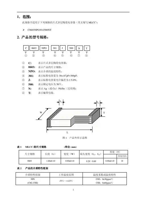
什么是多层片式瓷介电容器((MLCC)
多层瓷介电容器(MLCC)---简称片式电容器,是由印好电极(内电极)的陶
瓷介质膜片以错位的方式叠合起来,经过一次性高温烧结形成陶瓷芯片,再在
芯片的两端封上金属层(外电极),从而形成一个类似独石的结构体,故也叫
独石电容器。
片式电容器除有电容器“隔直通交”的通性特点外,其还有体积小,比容大,寿命长,可靠性高,适合表面安装等特点。
•随着世界电子行业的飞速发展,作为电子行业的基础元件,片式电容器也以惊人的速度向前发展,•
每年以10%~15%的速度递增。
目前,世界片式电容的需求量在2000 亿支以上,70%出自日本,其次是欧美和东南亚(含中国)。
随着片容产品可靠性和集成度的提高,其使用的范围越来越广,•广泛地应用于各种军民用电子整机和电子设备。
如电脑、电话、程控交换机、精密的测试仪器、雷达通信等。
片式电容器的基本结构简单的平行板电容器的基本结构是由一个绝缘的中间
介质层加外两个导电的金属电极,基本结构如下:
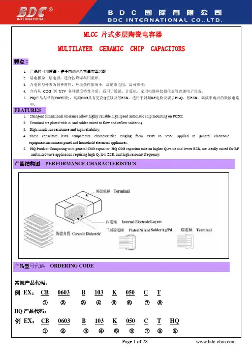
因此,多层片式陶瓷电容器的结构主要包括三大部分:陶瓷介质,金属内电极,金属外电极。
而多层片式陶瓷电容器它是一个多层叠合的结构,简单地说
它是由多个简单平行板电容器的并联体。
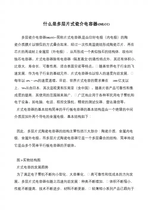
图3-实物结构图
片式电容的发展趋势
为了满足电子整机不断向小型化、大容量化、•高可靠性和低成本的方向发展。
多层片式电容器也随之迅速向前发展:种类不断增加,•体积不断缩小,性能不断提高,技术不断进步,材料不断更新,•轻薄短小系列产品已趋向于。
多层陶瓷片式电容多层陶瓷片式电容是一种常用的电子元件,广泛应用于电子设备中。
它具有体积小、容量大、质量轻、稳定性好等特点,被广泛应用于通信、计算机、汽车、医疗等领域。
本文将从多层陶瓷片式电容的结构、工作原理、特点及应用等方面进行介绍。
多层陶瓷片式电容由许多薄片状的陶瓷层和金属电极交替堆叠而成。
这些陶瓷层通常由氧化铁、氮化铁、氧化锆等材料制成,而金属电极则由铜、铝等导电材料制成。
这种层叠结构使得多层陶瓷片式电容能够在相对较小的体积中实现较大的电容量。
多层陶瓷片式电容的工作原理是基于电容器的原理。
当电容器两端施加电压时,金属电极上的电子会被电场作用而移动,形成电流。
而陶瓷层则起到绝缘的作用,阻止电流的流失。
由于多层陶瓷片式电容中陶瓷层的数量较多,因此电容量较大。
多层陶瓷片式电容具有许多特点。
首先,它具有良好的温度稳定性和频率特性,能够在不同的温度和频率下保持较稳定的电容值。
其次,多层陶瓷片式电容的损耗角正切值较小,能够提供较低的功率损耗。
此外,它还具有较高的绝缘电阻和较低的介质损耗,能够有效防止电流泄漏和能量损耗。
多层陶瓷片式电容在各个领域都有广泛的应用。
在通信领域,它常被用于电路板上的滤波器、耦合器等电子元件中,用于滤除噪声和提高信号质量。
在计算机领域,多层陶瓷片式电容被广泛应用于内存模块中,用于存储和传输数据。
在汽车领域,它常被用于汽车电子系统中,如发动机控制单元、车载娱乐系统等,用于提供稳定的电源和信号传输。
在医疗领域,多层陶瓷片式电容被应用于医疗设备中,如心脏起搏器、血压监测器等,用于提供稳定的电源和信号传输。
多层陶瓷片式电容是一种重要的电子元件,具有体积小、容量大、质量轻、稳定性好等特点。
它在通信、计算机、汽车、医疗等领域有广泛应用。
随着科技的不断进步,多层陶瓷片式电容的性能将进一步提高,应用领域也将更加广泛。
我们相信,在未来的发展中,多层陶瓷片式电容将发挥更大的作用,为人们的生活带来更多的便利和创新。

MLCC—搜狗百科 MLCC是⽚式多层陶瓷电容器英⽂缩写.(Multi-layer ceramic capacitors)⼀、瓷介的分类 陶瓷电容⼀般是以其温度系数作为主要分类。
Class I - ⼀类陶瓷(超稳定)EIA称之为COG 或NPO。
⼯作温度范围 -55℃~+125℃,容量变化不超过±30ppm/℃。
电容温度变化时,容值很稳定,被称作具有温度补偿功能,适⽤于要求容值在温度变化范围内稳定和⾼Q值的线路以及各种谐振线路。
Class II/III - ⼆/三类陶瓷(稳定)EIA标称的X7R表⽰温度下限为-55℃;上限温度为+125℃的⼯作温度范围内,容量最⼤的变化为 ±15%,Z5U、Y5V分别表⽰⼯作温度10~+85℃和-30~+85℃;容量最⼤变化为+22~-56%和30~82%,同属于⼆类陶瓷。
优点是体积利⽤率⾼,即在外型尺⼨相同时能提供更⾼的容值,适⽤于⾼容值和稳定性能要求不太⾼的线路。
⼆、瓷介代号陶瓷介质的代号是按其陶瓷材料的温度特性来命名的。
⽬前国际上通⽤美国EIA标准的叫法,⽤字母来表⽰。
常⽤的⼏种陶瓷材料的含义如下:Y5V:温度特性Y代表-25℃; 5代表+85℃;温度系数V代表-80%~+30%Z5U:温度特性Z代表+10℃; 5代表+85℃;温度系数U代表-56%~+22%X7R:温度特性X代表-55℃; 7代表+125℃温度系数R代表 ± 15%NP0:温度系数是30ppm/℃(-55℃~+125℃)三、⼀般电性能1、介电常数不同介质的类别有不同的表现效果。
环境因素,包括温度、电压、频率和时间(⽼化),对不同介质的电容有不同的影响。
介质常数(K值)越⾼,稳定性能、可靠性能和耐⽤性能便越差。
现代多层陶瓷电容器介质最常⽤有以下三类。
· COG或NPO(超稳定) K值10~100· X7R(稳定)K值2000~4000· Y5V或Z5U(⼀般⽤途)K值5000~250002、绝缘电阻(IR)即介质直流电阻,通常测量⽅法是以额定电压将电容充电⼀分钟,电容充电以后测量其漏电电流。
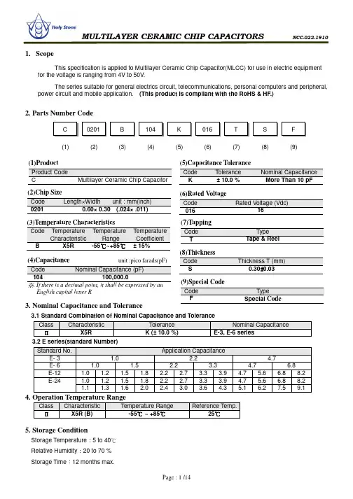
1. ScopeThis specification is applied to Multilayer Ceramic Chip Capacitor(MLCC) for use in electric equipment for the voltage is ranging from 4V to 50V.The series suitable for general electrics circuit, telecommunications, personal computers and peripheral, power circuit and mobile application. (This product is compliant with the RoHS & HF.)2. Parts Number Code3. Nominal Capacitance and Tolerance3.1 Standard Combination of Nominal Capacitance and ToleranceClass CharacteristicTolerance Nominal CapacitanceⅡX5RK (± 10.0 %)E-3, E-6 series3.2 E series(standard Number) Standard No.Application CapacitanceE- 3 1.02.24.7E- 6 1.0 1.52.23.34.76.8E-12 1.0 1.2 1.5 1.8 2.2 2.7 3.3 3.9 4.7 5.6 6.8 8.2 E-241.0 1.2 1.5 1.82.2 2.73.3 3.94.75.66.8 8.2 1.1 1.31.62.02.43.0 3.64.35.16.27.5 9.14. Operation Temperature RangeClassCharacteristic Temperature Range Reference Temp.Ⅱ X5R (B)-55 ~ +85℃℃25℃5. Storage ConditionStorage Temperature :5 to 40℃ Relative Humidity :20 to 70 % (1) (2) (3) (4) (5)(6)(7)(6)Rated VoltageCode Rated Voltage (Vdc)01616(1)ProductProduct Code C Multilayer Ceramic Chip Capacitor (3)Temperature CharacteristicsCode Temperature CharacteristicTemperature Range TemperatureCoefficientB X5R -55℃~+85℃ ± 15%(4)Capacitance unit :pico farads(pF) Code Nominal Capacitance (pF) 104 100,000.0※. If there is a decimal point, it shall be expressed by an English capital letter R(5)Capacitance ToleranceCode Tolerance Nominal Capacitance K± 10.0 %More Than 10 pF(7)TappingCode Type TTape & Reel(2)Chip Size Code Length×Width unit : mm(inch)02010.60× 0.30 (.024× .011)(8)(9)(8)ThicknessCode Thickness T (mm)S0.30±0.03(9)Special CodeCode TypeFSpecial Code6. Dimensions6.1 Configuration and Dimension :Unit:mmTYPE LW TB (min)BW (min) 02010.60± 0.030.30± 0.030.30± 0.030.200.106.2 Termination Type :External Electrodes BarrierInner ElectrodesPolymer Electrodes (If applicable)7. PerformanceFig.1P.C. Board for Bending Strength TestMaterial : Glass Epoxy Substrate: Solder ResistTest SubstrateMaterial : Glass Epoxy Substrate: Copper (Thickness : 0.035mm)Thickness : 1.6 mmUnit:mmType A B C 0201 0.2 0.9 0.4 0402 0.5 1.5 0.6 0603 1.0 3.0 1.0 0805 1.2 4.0 1.6 1206 2.2 5.0 2.0 1210 2.2 5.0 2.9 1808 3.5 7.0 2.5 1812 3.5 7.0 3.7 2208 4.5 8.0 2.5 2211 4.5 8.0 3.0 22204.58.05.68. Packing8.1 Bulk PackingAccording to customer request. 8.2 Chip Capacitors Tape Packing8.3 Material And QuantityTape Material 0201 0402 0603/0805 ≦T 0.33mm ≦T 0.55mm ≦T 1.00mm T >1.00mm Paper 15,000 pcs/Reel 10,000 pcs/Reel 4,000 pcs/Reel NAPlasticNA NA NA 3,000 pcs/ReelTape Material 1206≦T 1.00mm 1.00mm <≦T 1.25mmT >1.25mmPaper 4,000 pcs/ReelNANAPlastic NA3,000 pcs/Reel 2,000 pcs/ReelTape Material 1812/2211/2220 1825/2225 2208 T ≦2.20mm T >2.20mm T ≦2.20mm T >2.20mm T ≦2.20mm Paper NA NA NA NANAPlastic 1,000 pcs/Reel 700 pcs/Reel 700 pcs/Reel400 pcs/Reel 1,000 pcs/Reel NA :Not Available8.4 Cover Tape Reel Off Force8.4.1 Peel-Off Force5 g·≦f Peel-≦Off Force 70 g·f 8.4.2 Measure MethodTape Material 1808/1210≦T 1.25mm1.25mm <≦T2.40mmT >2.40mmPaper NANANAPlastic 3,000 pcs/Reel1,000/2,000 pcs/Reel500/1,000 pcs/Reel8.5 Paper TapeUnit:mm8.6 Plastic TapeUnit:mm TYPE A B C DE 0201 0.37± 0.1 0.67± 0.1 4.00± 0.1 2.00± 0.052.00± 0.10402 0.61± 0.1 1.20± 0.1 0603 1.10± 0.2 1.90± 0.2 4.00± 0.10805 1.50± 0.2 2.30± 0.2 1206 1.90± 0.2 3.50± 0.2 1210 2.90± 0.2 3.60± 0.2 TYPE FG H It0201 1.75± 0.103.50± 0.058.0± 0.30 φ1.50 +0.10/-0 1.10 max.0402 0603 0805 1206 1210Type A B C D E F 0805 1.5±0.2 2.3±0.2 4.0± 0.12.0± 0.054.0± 0.11.75± 0.11206 1.9±0.2 3.5±0.2 1210 2.9±0.2 3.6±0.2 1808 2.5±0.2 4.9±0.2 1812 3.6±0.2 4.9±0.2 8.0± 0.11825 6.9±0.2 4.9±0.2 2208 2.5±0.2 6.1±0.2 2211 3.2±0.2 6.1±0.2 2220 5.4±0.2 6.1±0.2 22256.9±0.26.1±0.28.7 Reel DimensionsReel Material :PolystyreneType G H IJ t O 0805 3.5± 0.058.0± 0.3φ1.5+0.1/-03.0 max.0.3 max.1.0± 0.11206 1210 1808 5.5± 0.05 12.0 ± 0.3 4.0 max. 1.5± 0.11812 1825 2208 2211 2220 2225Type AB C DE W 0201 φ382 max φ50 min φ13± 0.5φ21± 0.82.0±0.510± 0.150402 0603 0805 1206 1210 1808 φ178±2.0 φ60±2.0 13±0.31812 1825 2208 2211 2220 2225Unit:mmPrecautionary Notes:1. StorageStore the capacitors where the temperature and relative humidity don’t exceed 40°C and 70%RH. Werecommend that the capacitors be used within 12 months from the date of manufacturing. Store the products in the original package and do not open the outer wrapped, polyethylene bag, till just before usage. If it is open, seal it as soon as possible or keep it in a desiccant with a desiccation agent.2. Construction of Board PatternImproper circuit layout and pad/land size may cause excessive or not enough solder amount on the PC board. Not enough solder may create weak joint, and excessive solder may increase the potential of mechanical or thermal cracks on the ceramic capacitor. Therefore we recommend the land size to be as shown in the following table: 2.1 Size and recommend land dimensions for reflow soldering2.2 Mechanical strength varies according to location of chip capacitors on the P .C. board.Design layout of components on the PC board such a way to minimize the stress imposed on the components, upon flexure of the boards in depanelization or other processes.Component layout close to the edge of the board or the “depanelization line” is not recommended. Susceptibility to stress is in the order of: a>b>c and d>eEIA Code Chip (mm) Land (mm) L W A B C D E 0201 0.60 0.30 0.2~0.3 0.2~0.4 0.2~0.4 -- -- 0402 1.00 0.50 0.3~0.5 0.3~0.5 0.4~0.6 -- -- 0603 1.60 0.80 0.4~0.6 0.6~0.7 0.6~0.8 -- -- 0805 2.00 1.25 0.7~0.9 0.6~0.8 0.8~1.1 -- -- 1206 3.20 1.60 2.2~2.4 0.8~0.9 1.0~1.4 1.0~2.0 3.2~3.7 1210 3.20 2.50 2.2~2.4 1.0~1.2 1.8~2.3 1.0~2.0 4.1~4.6 1808 4.60 2.00 2.8~3.4 1.8~2.0 1.5~1.8 1.0~2.8 3.6~4.1 1812 4.60 3.20 2.8~3.4 1.8~2.0 2.3~3.0 1.0~2.8 4.8~5.3 1825 4.60 6.35 2.8~3.4 1.8~2.0 5.1~5.8 1.0~4.0 7.1~8.3 2208 5.70 2.00 4.0~4.6 2.0~2.2 1.5~1.8 1.0~4.0 3.6~4.1 2211 5.70 2.80 4.0~4.6 2.0~2.2 2.0~2.6 1.0~4.0 4.4~4.9 2220 5.70 5.00 4.0~4.6 2.0~2.2 3.5~4.8 1.0~4.0 6.6~7.1 2225 5.70 6.354.0~4.62.0~2.2 5.1~5.8 1.0~4.07.1~8.32.3 Layout Recommendation3. Mounting3.1 Sometimes crack is caused by the impact load due to suction nozzle in pick and place operation.In pick and place operation, if the low dead point is too low, excessive stress is applied to component. This maycause cracks in the ceramic capacitor, therefore it is required to move low dead point of a suction nozzle to the higher level to minimize the board warp age and stress on the components. Nozzle pressure is typically adjusted to 1N to 3N (static load) during the pick and place operation.3.2 Amount of Adhesivea0.2mm min. b 70 ~ 100 µm cDo not touch the solder landExample : 0805 & 12064. Soldering4.1. Wave SolderingMost of components are wave soldered with solder at Peak Temperature.. Adequate care must be taken to prevent the potential of thermal cracks on the ceramic capacitors. Refer to the soldering methods below for optimum soldering benefits.Recommend flow soldering temperature ProfileRecommended solder compositions Sn-37Pb (Pb - Sn Solder)Sn-3.0Ag-0.5Cu (Lead Free Solder)To optimize the result of soldering, proper preheating is essential: 1) Preheat temperature is too lowa. Flux flows to easilyb. Possibility of thermal cracks2) Preheat temperature is too higha. Flux deteriorates even when oxide film is removedb. Causes warping of circuit boardc. Loss of reliability in chip and other componentsCooling Condition:Natural cooling using air is recommended. If the chips are dipped into a solvent for cleaning, the temperature difference (ΔT) between the solvent and the chips must be less than 100°C.4.2 Reflow SolderingPreheat and gradualincrease in temperature to the reflow temperature is recommended to decrease the potential of thermal crack on the components. The recommended heating rate depends on the size of component, however it should not exceed 3°C/Sec.Recommend reflow profile for Lead-Free soldering temperature Profile (J-STD-020D)Soldering Method Change in Temp.( )℃1206 and Under Δ≦T 190 ℃1210 and Over Δ≦T 130 ℃Soldering Method Peak Temp.( ℃) / Duration (sec)1206 and Under ∆T ≤ 100~130 max. Pb-Sn Solder 250℃(max.) / 3sec(max.) Lead Free Solder 260℃(max.) / 5sec(max.) ※ The cycles of soldering : Twice (max.)Soldering T e m p e r a t u r e (°C )T e m p e r a t u r e (°C )4.3 Hand SolderingSudden temperature change in components, results in a temperature gradient recommended in the following table, and therefore may cause internal thermal cracks in the components. In general a hand soldering method is not recommended unless proper preheating and handling practices have been taken. Care must also be taken not to touch the ceramic body of the capacitor with the tip of solder Iron.Soldering Method Change in Temp.( )℃1206 and Under Δ≦T 150 ℃1210 and Over Δ≦T 130 ℃How to Solder Repair by Solder Iron1) Selection of the soldering iron tipThe required temperature of solder iron for any type of repair depends on the type of the tip, the substrate material, and the solder land size.2) recommended solder iron conditiona.) Preheating Condition:Board and components should be preheated sufficiently at 150°C or over,and soldering should be conducted with soldering iron as boards and components are maintainedat sufficient temperatures.b.) Soldering iron power shall not exceed 30 W.c.) Soldering iron tip diameter shall not exceed 3mm.d.) Temperature of iron tip shall not exceed 350°C to perform the process within 5 seconds.(refer to MIL-STD-202G)f.) Do not touch the ceramic body with the tip of solder iron. Direct contact of the soldering iron tip to ceramicbody may cause thermal cracks.g.) After soldering operation, let the products cool down gradually in the room temperature.5. Handling after chip mounted5.1 Proper handling is recommended, since excessive bending and twist of the board, depends on the orientationof the chip on the board, may induce mechanical stress and cause internal crack in the capacitor.Temperature(°C)200→Higher potential of crack Lower potential of crack ╳5.3 Mechanical stress due to warping a (a) Crack occurrence ratio will be in (b) Crack occurrence ratio will be in :Tensile Stress ╳6. Handling of Loose Chip Capacitor 6.1 If dropped the chip capacitor may c6.2 In piling and stacking of the P .C. bo may hit the chip capacitor mounted7. Safekeeping condition and period For safekeeping of the products, we re under humidity of 20 to 70% RH. The sing and torsion.be increased by manual separation.be increased by tensile force , rather than compressiv s○ :Compressive Stress tor may crack. .C. boards after mounting for storage or handling, the unted on another board to cause crack.we recommend to keep the storage temperature betwe The shelf life of capacitors is 12 months. ressive force.ess, the corner of the P .C. boardbetween +5 to +40°C and Crack。
多层片式陶瓷电容器执行标准总规范:GB/T2693-2001《电子设备用固定电容器第1部分:总规范》分规范:GB/T9324-1996《电子设备用固定电容器第10部分:分规范》GB/T9325-1996《电子设备用固定电容器第10部分:空白详细规范》分类介绍a、电解质种类容量温度特性是选用电介质种类的一个重要依据。
NPO(CG):I类电介质,电气性能最稳定,基本上不随温度、电压、时间的改变;属超稳定型、低损耗电容材料类型,适用于对稳定性、可靠性要求较高的高频、特高频、甚高频的电路。
产品应用:振荡器、混频器、中频/高频/甚高频/超高频放大器、低噪声放大器、时间电路、高频滤波电路、高频耦合。
X7R(2X1):II类电介质,电气性能较稳定,随温度、电压、时间的改变,其特有性能变化并不显著,属稳定型电容材料类型,适用于隔离、耦合、旁路、滤波电路及可靠性要求较高的中高频电路。
产品应用:电源(滤波、旁路)电路、时间电路、储能电路、中频/低频放大器(隔直、耦合、阻抗匹配),高频开关电源(S.P.S)、DC/DC变换器、滤波、旁路电路、隔直、阻抗匹配电路。
Y5V(2F4):III类电介质,具有较高的介电常数,常用于生产比容比较大的、标称容量较高的大容量电容产品;由于其特有的电介质性能,因而能造出容量比NPO更大的电容器。
属低频通用型电容材料类型,由于成本较低,广泛用于对容量、损耗要求偏低的电路。
产品应用:电源滤波电路、隔直、阻抗匹配电路。
b、电容量与偏差电容量与偏差的选择取决于电路的要求,特别提示,在相同尺寸和容量规格下,偏差较大的电容器的价格相对便宜。
c、电压额定电压的选择也取决于电路本身的要求,电容的耐压虽然在设计时已有一定的安全系数,但电容器额定电压的选择仍须高于实际工作电压。
d、片状电容器的端头电极:片状电容器端头电极的选择至关重要!全银端头:生产工艺简单、成本较低,耐焊性较差、端头物理强度也低,焊接时温度要适当,焊接速度要快,否则会出现银锡熔融现象而损坏端头。
北京芯联科泰电子有限公司贴片叠层瓷介电容器(SMD贴片电容)详细介绍:贴片电容全称:多层(积层,叠层)片式陶瓷电容器,也称为贴片电容,片容。
英文缩写:MLCC。
基本概述贴片电容(多层片式陶瓷电容器)是目前用量比较大的常用元件,就AVX公司生产的贴片电容来讲有NPO、X7R、Z5U、Y5V等不同的规格,不同的规格有不同的用途。
下面我们仅就常用的NPO、X7R、Z5U和Y5V来介绍一下它们的性能和应用以及采购中应注意的订货事项以引起大家的注意。
不同的公司对于上述不同性能的电容器可能有不同的命名方法,这里我们引用的是AVX公司的命名方法,其他公司的产品请参照该公司的产品手册尺寸贴片电容的尺寸表示法有两种,一种是英寸为单位来表示,一种是以毫米为单位来表示,贴片电容的系列型号有0402、0603、0805、1206、1210、1808、1812、2010、2225、2512,是英寸表示法, 04 表示长度是0.04 英寸,02 表示宽度0.02 英寸,其他类同型号尺寸(mm)英制尺寸公制尺寸长度及公差宽度及公差厚度及公差0402 1005 1.00±0.05 0.50±0.05 0.50±0.050603 1608 1.60±0.10 0.80±0.10 0.80±0.100805 2012 2.00±0.20 1.25±0.20 0.70±0.20 1.00±0.20 1.25±0.201206 3216 3.00±0.30 1.60±0.20 0.70±0.20 1.00±0.20 1.25±0.201210 3225 3.00±0.30 2.54±0.30 1.25±0.30 1.50±0.301808 4520 4.50±0.40 2.00±0.20 ≤2.001812 4532 4.50±0.40 3.20±0.30 ≤2.502225 5763 5.70±0.50 6.30±0.50 ≤2.503035 7690 7.60±0.50 9.00±0.05 ≤3.00命名贴片电容的命名所包含的参数有贴片电容的尺寸、做这种贴片电容用的材质、要求达到的精度、要求的电压、要求的容量、端头的要求以及包装的要求。
多层陶瓷片式电容1. 介绍多层陶瓷片式电容是一种常见的 passives 部件,用于各种电子设备中,如电源管理、通信设备、计算机和消费类电子产品等。
本文将详细探讨多层陶瓷片式电容的结构、工作原理、特点以及在不同应用中的优势。
2. 结构2.1 外观多层陶瓷片式电容通常由多个陶瓷层和金属电极组成,外观呈矩形或方形,容量范围从几皮法拉到几微法拉不等。
其尺寸一般小于传统的电解电容器。
2.2 材料陶瓷片式电容通常由高介电常数的陶瓷材料制成,如二氧化铁、二氧化钛等。
这些材料具有优异的绝缘性能和高温稳定性,能够满足各种应用的要求。
2.3 内部结构多层陶瓷片式电容的内部结构由交替排列的陶瓷层和金属电极组成。
陶瓷层可以看作是绝缘层,而金属电极用来引导电流。
电极通过多个孔穿过陶瓷层,形成电容器的结构。
3. 工作原理多层陶瓷片式电容的工作原理基于电介质的极化现象。
当电压施加在电容器的两个不同的端口上时,陶瓷材料中的电介质会极化,导致电荷在电容器内部的陶瓷层和金属电极之间移动。
这种电荷的分布在电压变化时发生变化,从而导致电容器存储和释放电荷的能力。
4. 特点多层陶瓷片式电容具有以下一些特点: 1. 高精度:制造过程精确,使得电容器能够达到较高的精度。
2. 高频特性:陶瓷片式电容的快速响应和低失真使其在高频电路中得到广泛应用。
3. 耐高温:陶瓷材料具有很好的高温稳定性,能够在高温环境下正常工作。
4. 无极性:与电解电容器不同,多层陶瓷片式电容没有极性限制,可以在电路中的任何方向连接。
5. 应用多层陶瓷片式电容由于其优异的性能,在各种电子设备中被广泛应用,主要包括以下几个方面: 1. 电源管理:多层陶瓷片式电容被用作稳压器和滤波器,用于稳定电源电压和滤除噪声。
2. 通信设备:多层陶瓷片式电容在无线通信中扮演重要角色,例如用于滤波、解调和射频调谐等。
3. 计算机:多层陶瓷片式电容被广泛应用于计算机内存模块、主板和硬盘驱动器等电路中。
多层片式陶瓷电容器(MLCC)的研究进展及发展趋势多层片式陶瓷电容器(MLCC)是片式元件的一个重要门类,由于具有结构紧凑、体积小、比容高、介电损耗低、价格便宜等诸多优点,被大量应用在计算机、移动电话、收音机、扫描仪、数码相机等电子产品中。
MLCC特别适合片式化表面组装,可大大提高电路组装密度,缩小整机体积,这一突出特性使MLCC成为当今世界上发展最快、用量最大的片式电子元件。
MLCC的应用领域决定了其介质材料必须具有以下性能:(1)高介电常数MLCC的比容与材料的介电常数关系如下:C为电容,V为体积,C/V为比电容,t为介电层厚度,ε为介电常数。
在介电层厚度确定的情况下,材料的介电常数越高,电容器比电容越大。
介电材料的介电常数越高,越易于实现电容器的小型化,这是目前电容器的一个发展方向,自从MLCC问世以来,其比容一直不断上升,介电层的厚度不断下降。
如图1所示。
(2)良好的介温特性介温特性用来描述电容随温度变化情况。
一般来说,在工作状态下,电容器的电容随温度的变化越小越好。
由于电容随温度发生变化来源于介质材料介电常数的变化,因此要求节电材料具有良好的介温特性。
(3)高绝缘电阻率(4)介电损耗小,抗老化1.研究进展MLCC用高介电常数的介电材料可以归结为以下三个体系:BaTiO3系材料;(Ba,Ca)(Ti,Zr)O3系材料;复合含Pb 钙钛矿系材料。
1.1BaTiO3系材料BaTiO3系材料是最早研究的用于MLCC的介电材料,也是最早实现商业化的MLCC用介电材料。
从20世纪60年代初期到70年代末,为了实现MLCC贱金属化,降低电容器的成本,人们对BaTiO3系材料的研究多集中在抗还原方面。
常用的手段是向BaTiO3中添加过渡元素的氧化物,这些元素的离子在还原气氛下俘获电子发生变价,从而提高还原烧结BaTiO3材料的绝缘电阻。
但是由于受主掺杂BaTiO3材料中氧空位的迁移,使用后不久,材料的绝缘电阻就大幅下降,MLCC的性能严重劣化。
多层片式陶瓷电容器
执行标准
总规范:GB/T2693-2001《电子设备用固定电容器第1部分:总规范》
分规范:GB/T9324-1996《电子设备用固定电容器第10部分:分规范》GB/T9325-1996《电子设备用固定电容器第10部分:空白详细规范》
分类介绍
a、电解质种类
容量温度特性是选用电介质种类的一个重要依据。
NPO(CG):I类电介质,电气性能最稳定,基本上不随温度、电压、时间的改变;属超稳定型、低损耗电容材料类型,适用于对稳定性、可靠性要求较高的高频、特高频、甚高频的电路。
产品应用:振荡器、混频器、中频/高频/甚高频/超高频放大器、低噪声放大器、时间电路、高频滤波电路、高频耦合。
X7R(2X1):II类电介质,电气性能较稳定,随温度、电压、时间的改变,其特有性能变化并不显著,属稳定型电容材料类型,适用于隔离、耦合、旁路、滤波电路及可靠性要求较高的中高频电路。
产品应用:电源(滤波、旁路)电路、时间电路、储能电路、中频/低频放大器(隔直、耦合、阻抗匹配),高频开关电源(S.P.S)、DC/DC变换器、滤波、旁路电路、隔直、阻抗匹配电路。
Y5V(2F4):III类电介质,具有较高的介电常数,常用于生产比容比较大的、标称容量较高的大容量电容产品;由于其特有的电介质性能,因而能造出容量比NPO更大的电容器。
属低频通用型电容材料类型,由于成本较低,广泛用于对容量、损耗要求偏低的电路。
产品应用:电源滤波电路、隔直、阻抗匹配电路。
b、电容量与偏差
电容量与偏差的选择取决于电路的要求,特别提示,在相同尺寸和容量规格下,偏差较大的电容器的价格相对便宜。
c、电压
额定电压的选择也取决于电路本身的要求,电容的耐压虽然在设计时已有一定的安全系数,但电容器额定电压的选择仍须高于实际工作电压。
d、片状电容器的端头电极:片状电容器端头电极的选择至关重要!
全银端头:生产工艺简单、成本较低,耐焊性较差、端头物理强度也低,焊接时温度要适当,焊接速度要快,否则会出现银锡熔融现象而损坏端头。
钯全银端头:针对全银的缺点而改进,其耐焊性能、端头强度均获改善,但可焊性随存放时间而改变。
三层电镀端头:(银、镍、锡)耐焊性性能优越,端头物理强度高,可焊性好。
适用于自动贴片机焊接、波峰焊接、再流焊接及手工焊接等诸多焊接工艺,符合SMT操作条件。
通用型NPO(COG)片容
NPO(COG):通用型COG片容属于I类高频电容器,其电容量非常稳定,几乎不随温度、电压和时间的变化而变化。
尤其适用于高频电子线路。
特性:具有高的电容量稳定性,在-55℃~125℃工作范围内,其温度系数为0±30ppm/℃、0±60ppm/℃。
叠层独石结构,具有高可靠性。
优良的焊接性和耐焊性,适用于回流焊和波峰焊。
应用:适用于各种高频电子线路。
尺寸规格:
0603 0.06×0.03(英寸) 1.6×0.8(mm)
0805 0.08×0.05(英寸) 2.0×1.25(mm)
1206 0.12×0.06(英寸) 3.2×1.6(mm)
1210 0.12×0.10(英寸) 3.2×2.5(mm)
1812 0.18×0.12(英寸) 4.5×3.2(mm)
2225 0.22×0.25(英寸) 5.7×6.4(mm)
3035 0.30×0.35(英寸) 7.6×9.0(mm)
标称容量(PF):102 10×102 103 10×103
误差:
B ±0.10PF
C ±0.25PF
D ±0.50PF
F ±1.0%
G ±2.0%
J ±5.0%
K ±10%
M ±20%
端头材料:
S 全银
N 三层电镀额定电压(V):160 16×100 250 25×100 500 50×100 630 63×100 101 10×101 201 20×101 501 50×101 102 10×102 202 20×102
通用型X7R片容
通用型X7R片容属于II类低频电容器,其电容量相对稳定。
特性:具有较高的电容量且较稳定,在-55℃~125℃工作范围内,其温度特性为±15%。
叠层独石结构,具有高可靠性。
优良的焊接性和耐焊性,适用于回流焊和波峰焊。
应用:适用于各种滤波,耦合电路。
尺寸规格:
0603 0.06×0.03(英寸) 1.6×0.8(mm)
0805 0.08×0.05(英寸) 2.0×1.25(mm)
1206 0.12×0.06(英寸) 3.2×1.6(mm)
1210 0.12×0.10(英寸) 3.2×2.5(mm)
1812 0.18×0.12(英寸) 4.5×3.2(mm)
2225 0.22×0.25(英寸) 5.7×6.4(mm)
3035 0.30×0.35(英寸) 7.6×9.0(mm)
标称容量(PF):
102 10×102
224 22×104
误差:
K ±10%
M ±20%
S +50%/-20%端头材料:
S 全银
N 三层电镀额定电压(V):160 16×100 250 25×100 500 50×100 630 63×100 101 10×101 201 20×101 501 50×101 102 10×102 202 20×102
通用型Y5V片容
通用型Y5V片容属于II类低频电容器,其电容量受湿度、电压、时间变化大。
特性:在-25℃~85℃工作范围内,其温度特性为+30%,-80%。
叠层独石结构,具有高可靠性。
优良的焊接性和耐焊性,适用于回流焊和波峰焊。
应用:适用于各种滤波线路。
尺寸规格:
0603 0.06×0.03(英寸) 1.6×0.8(mm)
0805 0.08×0.05(英寸) 2.0×1.25(mm)
1206 0.12×0.06(英寸) 3.2×1.6(mm)
1210 0.12×0.10(英寸) 3.2×2.5(mm)
1812 0.18×0.12(英寸) 4.5×3.2(mm)
2225 0.22×0.25(英寸) 5.7×6.4(mm)
3035 0.30×0.35(英寸) 7.6×9.0(mm)
标称容量(PF):
102 10×102
224 22×104
误差:
K ±10%
M ±20%
S +50%/-20%
Z +80%/-20%
P +100%/0
端头材料:
S 全银
N 三层电镀
额定电压(V):
160 16×100
250 25×100
500 50×100
630 63×100
101 10×101
201 20×101
501 50×101
102 10×102
202 20×102
火炬产品外形尺寸/容量范围/额定电压
NPO外形尺寸/容值范围/额定电压:
电容值:0R5、1R0、1R2、1R5、1R8、2R2、2R7、3R3、3R9、4R7、5R6、6R8、8R2、100、120、150、180、220、270、330、390、470、560、680、820、101、121、151、181、221、271、331、391、471、561、681、821、102、122、152、182、222、272、332、392、472、
X7R、X5R外形尺寸/容值范围/额定电压:
电容值:221、271、331、391、471、561、681、821、102、122、152、182、222、272、332、392、472、562、682、822、103、123、153、183、223、273、333、393、473、563、683、823、104、124、154、184、224、274、334、394、474、564、684、824、105、125、155、
X7R、X5R外形尺寸/容值范围/额定电压:
电容值:222、272、332、392、472、562、682、822、103、123、153、183、223、273、333、393、473、563、683、823、104、124、154、184、224、274、334、394、474、564、684、824、105、125、155、185、225、275、335、395、475、565、685、825、106、126、156、。