Typical current harmonics ATV V01.00
- 格式:pdf
- 大小:171.45 KB
- 文档页数:13

SPECIFICATIONSNI USB-6002Low-Cost DAQ USB DeviceThe following specifications are typical at 25 °C, unless otherwise noted. For more information about the NI USB-6002, refer to the NI USB-6001/6002/6003 User Guide available at /manuals.Analog InputNumber of channelsDifferential4....................................................................Single-ended8....................................................................ADC resolution16-bit ............................................................................Maximum sample rate (aggregate)50 kS/s ............................................................................Converter type Successive approximation ............................................................................ ............................................................................AI FIFO2,047 samplesTrigger sources Software, PFI 0, PFI 1 ........................................................................................................................................................Input range±10 VWorking voltage±10 V ............................................................................Overvoltage protectionPowered-on±30 V....................................................................Powered-off±20 V....................................................................Input impedance>1 GΩ............................................................................Input bias current±200 pA ............................................................................Absolute accuracy....................................................................Typical at full scale 6 mV26 mVMaximum over temperature,....................................................................full scaleSystem noise0.4 mVrms.................................................................... ............................................................................DNL16-bit, no missing codesINL±1.8 LSB ............................................................................CMRR56 dB (DC to 5 kHz) ............................................................................Bandwidth300 kHz ............................................................................Analog OutputAnalog outputs2 ............................................................................DAC resolution16-bit ............................................................................Output range±10 V ............................................................................Maximum update rate 5 kS/s simultaneous per channel, hardware-............................................................................timedAO FIFO2,047 samples ............................................................................ ............................................................................Trigger sources Software, PFI 0, PFI 1Output current drive±5 mA ............................................................................Short circuit current±11 mA ............................................................................Slew rate 3 V/μs ............................................................................Output impedance0.2 Ω............................................................................2| | NI USB-6002 SpecificationsAbsolute accuracy (no load)Typical at full scale8.6 mV....................................................................Maximum over temperature, full scale32 mV....................................................................DNL16-bit, no missing codes ............................................................................INL±4 LSB ............................................................................Power-on state0 V ............................................................................ ............................................................................Startup glitch-7 V for 10 µsTimebaseNote The following specifications apply to the sampling accuracy for hardware-timed analog input and analog output.Timebase frequency80 MHz ............................................................................Timebase accuracy±100 ppm ............................................................................ ............................................................................Timing resolution12.5 nsDigital I/O13 digital lines....................................................................Port 08 linesPort 1 4 lines....................................................................Port 2 1 lines....................................................................FunctionP0.<0..7>Static digital input/output....................................................................P1.0Static digital input/output........................................................................................................................................P1.1/PFI 1Static digital input/output, counter source ordigital triggerNI USB-6002 Specifications| © National Instruments| 3....................................................................P1.<2..3>Static digital input/outputP2.0/PFI 0Static digital input/output, counter source or ....................................................................digital triggerDirection control Each channel individually programmable as ............................................................................input or outputOutput driver type Each channel individually programmable as ............................................................................open collector or active driveAbsolute maximum voltage range-0.3 V to 5. 5 V with respect to D GND ............................................................................Pull-down resistor47.5 kΩ to D GND ............................................................................Power-on state Input ............................................................................Digital InputInput voltage range (powered on)0 to 5 V ............................................................................ ............................................................................Input voltage range (powered off)0 to 3.3 VInput voltage protection±20 V on two lines per port (maximum of five ............................................................................lines for all ports) for up to 24 hours Caution Do not leave a voltage above 3.3 V connected on any DIO line forextended periods of time when the device is powered off. This may lead to long termreliability issues. ............................................................................Minimum V IH 2.3 VMaximum V IL0.8 V ............................................................................Maximum input leakage currentAt 3.3 V0.8 mA....................................................................At 5 V 4.5 mA....................................................................Digital Output (Active Drive)Maximum V OL (4 mA)0.7 V ............................................................................Maximum V OL (1 mA)0.2 V ............................................................................Minimum V OH (4 mA) 2.1 V ............................................................................Minimum V OH (1 mA) 2.8 V ............................................................................ ............................................................................Maximum V OH 3.6 VMaximum output current per line±4 mA ............................................................................4| | NI USB-6002 SpecificationsDigital Output (Open Collector) ............................................................................Maximum V OL (4 mA)0.8 VMaximum V OL (1 mA)0.2 V ............................................................................Note Minimum Vdependent on user-provided pull-up resistor and voltagesource. Recommended pull-up resistor is 1 kΩ.Using a 1 kΩ pull-up resistor and 5 V voltagesource:Minimum V OH 3.5 V....................................................................Typical V OH 4.5 V....................................................................Maximum output (sinking) current per line-4 mA ............................................................................ ............................................................................Maximum pull-up voltage 5 VMaximum leakage currentAt 3.3 V0.8 mA........................................................................................................................................At 5 V 4.5 mACounterNumber of counters1 ............................................................................Resolution32-bit ............................................................................Counter measurements Edge counting, rising or falling ............................................................................Counter direction Count up ............................................................................ ............................................................................Counter source PFI 0 or PFI 1Maximum input frequency 5 MHz ............................................................................Minimum high pulse width100 ns ............................................................................ ............................................................................Minimum low pulse width100 nsNI USB-6002 Specifications| © National Instruments| 5+5 V Power SourceOutput voltage+5 V, ±3% ............................................................................Maximum current150 mA ............................................................................Overcurrent protection200 mA ............................................................................Short circuit current50 mA ............................................................................Overvoltage protection±20 V ............................................................................Bus InterfaceUSB specification USB Full Speed ............................................................................ ............................................................................USB bus speed12 Mb/sPhysical CharacteristicsDimensionsWithout screw terminal connector plugs75.4 mm × 86.2 mm × 23.6 mm, (2.97 in. ×....................................................................3.40 in. × 0.93 in.)With screw terminal connector plugs93.2 mm × 86.2 mm × 23.6 mm, (3.67 in. ×....................................................................3.40 in. × 0.93 in.)6| | NI USB-6002 SpecificationsFigure 1. NI USB-6002 DimensionsWeightWithout screw terminal connector plugs83 g (2.93 oz)....................................................................With screw terminal connector plugs105 g (3.70 oz)....................................................................I/O connectors: USB Micro-B receptacle, (1)16-position screw terminal plugsScrew-terminal wiring 1.31 to 0.08 mm2 (16 to 28 AWG)....................................................................Torque for screw terminals0.22 - 0.25 N · m (2.0 - 2.2 lb. · in.)....................................................................If you need to clean the module, wipe it with a dry towel.EnvironmentalTemperature (IEC 60068-2-1 andIEC 60068-2-2)Operating0 to 45 °C....................................................................Storage-40 to 85 °C....................................................................Humidity (IEC 60068-2-56)Operating 5 to 95% RH, noncondensing....................................................................Storage 5 to 90% RH, noncondensing....................................................................NI USB-6002 Specifications| © National Instruments| 7Pollution Degree (IEC 60664)2 ............................................................................Maximum altitude2,000 m ............................................................................Indoor use only.SafetyThis product meets the requirements of the following standards of safety for electrical equipment for measurement, control, and laboratory use:•IEC 61010-1, EN 61010-1•UL 61010-1, CSA 61010-1Note For UL and other safety certifications, refer to the product label or the OnlineProduct Certification section.Electromagnetic CompatibilityThis product meets the requirements of the following EMC standards for sensitive electrical equipment for measurement, control, and laboratory use:•EN 61326-1 (IEC 61326-1): Class A emissions; Basic immunity•EN 55011 (CISPR 11): Group 1, Class A emissions•EN 55022 (CISPR 22): Class A emissions•EN 55024 (CISPR 24): Immunity•AS/NZS CISPR 11: Group 1, Class A emissions•AS/NZS CISPR 22: Class A emissions•FCC 47 CFR Part 15B: Class A emissions•ICES-001: Class A emissionsNote In the United States (per FCC 47 CFR), Class A equipment is intended foruse in commercial, light-industrial, and heavy-industrial locations. In Europe,Canada, Australia, and New Zealand (per CISPR 11) Class A equipment is intendedfor use only in heavy-industrial locations.Note Group 1 equipment (per CISPR 11) is any industrial, scientific, or medicalequipment that does not intentionally generate radio frequency energy for thetreatment of material or inspection/analysis purposes.Note For EMC declarations and certifications, and additional information, refer tothe Online Product Certification section.8| | NI USB-6002 SpecificationsCE ComplianceThis product meets the essential requirements of applicable European Directives, as follows:•2006/95/EC; Low-V oltage Directive (safety)•2004/108/EC; Electromagnetic Compatibility Directive (EMC)Online Product CertificationTo obtain product certifications and the DoC for this product, visit /certification, search by model number or product line, and click the appropriate link in the Certification column. Environmental ManagementNI is committed to designing and manufacturing products in an environmentally responsible manner. NI recognizes that eliminating certain hazardous substances from our products is beneficial to the environment and to NI customers.For additional environmental information, refer to the Minimize Our Environmental Impact web page at /environment. This page contains the environmental regulations and directives with which NI complies, as well as other environmental information not included in this document.Waste Electrical and Electronic Equipment (WEEE) EU Customers This symbol indicates that waste products should be disposed ofseparately from municipal household waste according toWEEE Directive 2002/96/EC of the European Parliament and the Council on wasteelectrical and electronic equipment (WEEE). All products at the end of their lifecycle must be sent to a WEEE collection and recycling center. Proper WEEEdisposal reduces environmental impact and the risk to human health due topotentially hazardous substances used in such equipment. Your cooperation inproper WEEE disposal will contribute to the effective usage of natural resources. Forinformation about the available collection and recycling scheme in a particularcountry, go to /environment/weee.电子信息产品污染控制管理办法(中国RoHS)中国客户National Instruments符合中国电子信息产品中限制使用某些有害物质指令(RoHS)。
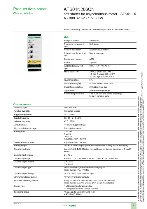
T h e i n f o r m a t i o n p r o v i d e d i n t h i s d o c u m e n t a t i o n c o n t a i n s g e n e r a l d e s c r i p t i o n s a n d /o r t e c h n i c a l c h a r a c t e r i s t i c s o f t h e p e r f o r m a n c e o f t h e p r o d u c t s c o n t a i n e d h e r e i n .T h i s d o c u m e n t a t i o n i s n o t i n t e n d e d a s a s u b s t i t u t e f o r a n d i s n o t t o b e u s e d f o r d e t e r m i n i n g s u i t a b i l i t y o r r e l i a b i l i t y o f t h e s e p r o d u c t s f o r s p e c i f i c u s e r a p p l i c a t i o n s .I t i s t h e d u t y o f a n y s u c h u s e r o r i n t e g r a t o r t o p e r f o r m t h e a p p r o p r i a t e a n d c o m p l e t e r i s k a n a l y s i s , e v a l u a t i o n a n d t e s t i n g o f t h e p r o d u c t s w i t h r e s p e c t t o t h e r e l e v a n t s p e c i f i c a p p l i c a t i o n o r u s e t h e r e o f .N e i t h e r S c h n e i d e r E l e c t r i c I n d u s t r i e s S A S n o r a n y o f i t s a f f i l i a t e s o r s u b s i d i a r i e s s h a l l b e r e s p o n s i b l e o r l i a b l e f o r m i s u s e o f t h e i n f o r m a t i o n c o n t a i n e d h e r e i n .Product data sheetCharacteristicsATS01N206QNsoft starter for asynchronous motor - ATS01 - 6A - 380..415V - 1.5..3 KWProduct availability: Non-Stock - Not normally stocked in distribution facilityMainRange of product Altistart 01Product or component typeSoft starterProduct destination Asynchronous motors Product specific applica-tionSimple machine Device short name ATS01Phase3 phase[Us] rated supply volt-age380...415 V - 10...10 %Motor power kW3 KW, 3 phase 380...415 V 1.5 KW, 3 phase 380...415 V 2.2 kW, 3 phase 380...415 V IcL starter rating 6 AUtilisation category AC-53B EN/IEC 60947-4-2Current consumption 30 A at nominal load Type of startStart with voltage rampPower dissipation in W4 W at full load and at end of starting 64 W in transient stateComplementaryAssembly style With heat sink Function available Integrated bypass Supply voltage limits 342…456 V Supply frequency 50...60 Hz - 5...5 %Network frequency 47.5...63 HzOutput voltage<= power supply voltage [Uc] control circuit voltage Built into the starter Starting time1 s / 1005 s / 2010 s / 10Adjustable from 1 to 10 s Deceleration time symb Adjustable from 1 to 10 sStarting torque 30...80 % of starting torque of motor connected directly on the line supply Discrete input type Logic LI1, LI2, BOOST) stop, run and boost on start-up functions <= 8 mA 27kOhm Discrete input voltage 24...40 VDiscrete input logic Positive LI1, LI2, BOOST < 5 V <= 0.2 mA > 13 V, >= 0.5 mA Discrete output current 2 A DC-133 A AC-15Discrete output type Open collector logic LO1 end of starting signal Relay outputs R1A, R1C NO Discrete output voltage 24 V 6...30 V) open collector logic Minimum switching current 10 mA 6 V DC relay outputsMaximum switching current Relay outputs 2 A 250 V AC cos phi = 0.5 20 ms inductive Relay outputs 2 A 30 V DC cos phi = 0.5 20 ms inductive Display type 1 LED green)starter powered up1 LED yellow)nominal voltage reached Tightening torque16.82…22.13 Lbf.In (1.9…2.5 N.m)4.43 lbf.in (0.5 N.m)Electrical connection 4 mm screw clamp terminal - rigid 1 1...10 mm² AWG 8 power circuitScrew connector - rigid 1 0.5...2.5 mm² AWG 14 control circuit4 mm screw clamp terminal - rigid 2 1...6 mm² AWG 10 power circuitScrew connector - rigid 2 0.5...1 mm² AWG 17 control circuitScrew connector - flexible with cable end 1 0.5...1.5 mm² AWG 16 control circuit4 mm screw clamp terminal - flexible without cable end 1 1.5...10 mm² AWG 8power circuitScrew connector - flexible without cable end 1 0.5...2.5 mm² AWG 14 control cir-cuit4 mm screw clamp terminal - flexible with cable end 2 1...6 mm² AWG 10 powercircuit4 mm screw clamp terminal - flexible without cable end 2 1.5...6 mm² AWG 10power circuitScrew connector - flexible without cable end 2 0.5...1.5 mm² AWG 16 control cir-cuitMarking CEOperating position Vertical +/- 10 degreeHeight 4.88 in (124 mm)Width 1.77 in (45 mm)Depth 5.16 in (131 mm)Net weight0.93 lb(US) (0.42 kg)Compatibility code ATS01N2Motor power range AC-3 1.1…2 KW 380…440 V 3 phase2.2…3 kW 380…440 V 3 phaseMotor starter type Soft starterEnvironmentElectromagnetic compatibility Conducted and radiated emissions level B CISPR 11Conducted and radiated emissions level B IEC 60947-4-2Damped oscillating waves level 3 IEC 61000-4-12Electrostatic discharge level 3 IEC 61000-4-2EMC immunity EN 50082-1EMC immunity EN 50082-2Harmonics IEC 1000-3-2Harmonics IEC 1000-3-4Immunity to conducted interference caused by radio-electrical fields level 3 IEC61000-4-6Immunity to electrical transients level 4 IEC 61000-4-4Immunity to radiated radio-electrical interference level 3 IEC 61000-4-3Micro-cuts and voltage fluctuation IEC 61000-4-11Voltage/current impulse level 3 IEC 61000-4-5Standards EN/IEC 60947-4-2Product certifications ULB44.1-96/ASME A17.5 for starter wired to the motor delta terminalCSAGOSTC-TickCCCIP degree of protection IP20Pollution degree 2 EN/IEC 60947-4-2Vibration resistance 1 gn 13…150 Hz)EN/IEC 60068-2-61.5 mm peak to peak 3…13 Hz)EN/IEC 60068-2-6Shock resistance15 gn 11 ms EN/IEC 60068-2-27Relative humidity5…95 % without condensation or dripping water EN/IEC 60068-2-3Ambient air temperature for operation14…104 °F (-10…40 °C) without)104…122 °F (40…50 °C) with current derating of 2 % per °C)Ambient air temperature for storage-13…158 °F (-25…70 °C) EN/IEC 60947-4-2Operating altitude<= 3280.84 ft (1000 m) without> 3280.84 ft (1000 m) with current derating of 2.2 % per additional 100 m Ordering and shipping detailsCategory22392 - ATSU01/ATS01 LOW HP SOFT STARTERSDiscount Schedule I11GTIN00785901457671Package weight(Lbs)0.50 kg (1.11 lb(US))Returnability NoCountry of origin DEOffer SustainabilityREACh Regulation REACh DeclarationREACh free of SVHC YesEU RoHS Directive Pro-active compliance (Product out of EU RoHS legal scope)EU RoHS Decla-rationToxic heavy metal free YesMercury free YesRoHS exemption information YesChina RoHS Regulation China RoHS DeclarationWEEE The product must be disposed on European Union markets following specificwaste collection and never end up in rubbish bins.Contractual warrantyWarranty18 monthsDimensions DrawingsDimensionsMounting on Symetrical (35 mm) RailScrew Fixing(1)Retractable fixingsConnections and SchemaExample of Manual ControlA1 :Soft start/soft stop unit (1)For type 2 coordination Q1 :Motor circuit-breaker F3 : 3 fast-acting fusesTechnical DescriptionFunction Diagram2-wire Control with DecelerationUs :Power supply voltage LED 1 :Green LED LI2 :Logic input R1 :Relay output LO1 :Logic output LED 2 :Yellow LED3-wire Control with DecelerationUs :Power supply voltage LED 1 :Green LED LI2,LI1 :Logic inputs R1 :Relay output LO1 :Logic output Um :Motor voltage LED 2 :Yellow LED。

THIS PAGE INTENTIONALLY LEFT BLANKFrequency Hopping with HittitePLLVCOsApplication Note1 Table of Contents1Table of Contents (2)2Overview (3)3Selecting the target frequency (3)3.1Applicable Products (3)4Manual VCO Calibration Options (4)4.1Manual Calibration with Direct LUT (4)4.2Manual Calibration with LUT Extrapolation (4)5Calibration with Direct LUT (5)5.1Divider Configuration (5)5.2Setting up the LUT table (5)5.3Programming the LUT frequency during operation (6)6Calibration with LUT Extrapolation (6)6.1Divider Configuration (6)6.2Setting up the LUT table (6)6.3Programming the LUT frequency during operation (8)7Frequently Asked Questions (9)Revision HistoryRevision Date DescriptionRev 1.0 August, 2013 First pre-releaseRev 2.0 May 2014 First release2 OverviewThe application note applies to frequency hopping and other time sensitive frequency tuning applications using Hittite’s narrowband, triband or wideband PLLVCOs.Typically applications using Hittite PLLVCOs use the built-in VCO frequency calibration function to lock to a new frequency. However, in many cases there are limitations on the time available to hop to a new frequency or between selected frequencies.This application note describes the methods to implement fast frequency hopping. Hittite recommends that customers with settling time requirements faster than 1msec contact Hittite Applications Support. Hittite PLLVCOs are capable of very fast settling times, well under 100usec in many cases, however, certain conditions on performance do exist. Our Applications Support team can advise how best to get the required performance.3 Selecting the target frequencyThe Hittite PLLVCOs have one or more VCO cores, depending on the total frequency range covered by the product. Each VCO core has an array of switched capacitors (often 5 capacitors, providing total of 25 or 32 possible capacitor settings per VCO core). The VCO auto-calibration routine selects the suitable capacitor setting for optimal VCO performance. This capacitor setting does not change for a given frequency, and is used across the whole operating temperature range.There are applications that need control over the time it takes to switch frequencies. For these applications, it is recommended to use a manual calibration routine. In manual calibration mode the user generates a look-up table (LUT) that stores the capacitor settings for each frequency of interest. The LUT can be generated at production test, or at bring-up of the system card. Upon frequency changes these settings are written directly to the device registers, thereby eliminating the need to run the auto-calibration routine.3.1 Applicable ProductsThis note applies to the following products:HMC820LP6CE HMC821LP6CE HMC822LP6CE HMC824LP6CEHMC826LP6CE HMC828LP6CE HMC829LP6GE HMC830LP6GEHMC831LP6CE HMC832LP6GE HMC833LP6GE HMC834LP6GEHMC835LP6GE HMC836LP6CE HMC837LP6CE HMC838LP6CEHMC839LP6CE HMC840LP6CE HMC1190LP6GE HMC1197LP7FE4 Manual VCO Calibration OptionsPrior to use, a device-specific LUT is created in the host controller, which associates all required frequencies to VCO capacitor settings. The manual calibration can be a one-time calibration occurring during the customer’s production test, supported by non-volatile memory in the host system. Alternatively, the system can be designed to perform a self-calibration on every power-up, supported by regular static memory in the host system. Both techniques offer reliable operation at all operating temperatures and over time, including aging effects.When the system needs to change frequency during regular operation, the correct VCO capacitor setting is selected from the LUT. The system then programs the required capacitor value into the VCO and programs the PLL divider registers as required for the frequency change. The frequency hop time using manual calibration is defined by the number of SPI writes, SPI clock speed and the normal PLL settling behavior.The look-up-table can be created in two ways:1. Manual calibration with direct LUT, which captures and stores settings for all required frequencies2. Manual calibration with LUT extrapolation, which captures and stores settings for limited numberof frequencies, and uses extrapolation to determine settings between these frequencies4.1 Manual Calibration with Direct LUT1. Program the required frequency with Auto-calibration enabled2. Wait for the Auto-calibration to complete3. Read the VCO capacitor setting selected by the Auto-calibration for that frequency4. Record the Frequency and Capacitor setting in the LUT5. Repeat 1 thru 4 for all required frequencies6. Once the LUT is completed, disable the VCO Auto-calibrationUse the table to select the appropriate VCO capacitor setting for the desired VCO frequency;4.2 Manual Calibration with LUT Extrapolation1. Program the VCO open loop with the internal preset voltage applied to the varactor. This centersthe VCO at mid-tuning voltage on each capacitor setting2. Program the required VCO capacitor setting3. Record the frequency of the VCO capacitor setting by using the error count feature4. Repeat steps 1 thru 3 for all possible capacitor settings5. Calculate the frequency half way between each VCO cap setting measured above, and store thefrequency in the LUT as the switching point between VCO capacitor settingsWhen complete, use the LUT to select the appropriate VCO capacitor setting for any desired VCO frequency, (fvco).5 Calibration with Direct LUTInformation below describes the calibration method in detail.5.1 Divider ConfigurationIn addition, to performing the Manual Calibration, two register setting changes are required for proper operation:1. Reg08h[8]=1 to “Disable Synchronous VCO Divider Reset”2. Reg0Bh[18:17]=10 to set “Mcounter (VCO Divider) Clock Gating” for N<10235.2 Setting up the LUT tableApply power to FPGA/microcontroller while keeping PLL+VCO product unpowered. Configure SPI signals going to PLL+VCO product and set all SPI digital signals low. Apply power to PLL+VCO product and cycle either SCK or SEN to configure the correct SPI programming protocol (not required for HMC835, HMC1190 and HMC1197). Then follow the steps outlined in the table below.Table 1. Calibration with Direct LUTStep Action Comments1 Initialize Initialize the device for normal operation with VCO Auto-calibration enabled2 Program the first frequency viaReg03h and Reg04h If the frequency requires the use of the VCO Output Divider, the divider must be set prior to programming to ensure correct VCO and VCO capacitor selection3 Wait until the device has locked to thespecified frequency Poll the LD register to ensure device is locked to selected frequency4 Read Reg10h & manipulate data forstorage in the LUT For Wideband PLL+VCO & Clock Generation devices (HMC829, HMC830, HMC832, HMC833, HMC834, HMC1032, HMC1033, HMC1034, HMC1035):[Reg10h x 2^8]For Wideband PLL+VCO HMC835 and Wideband PLL+VCO with Integrated Mixer devices HMC1190, HMC1197:[Reg10h[8:1] x 2] + E4A00hFor Narrowband, Triband devices (HMC820, HMC821, HMC822, HMC824, HMC826, HMC828, HMC831, HMC836, HMC837, HMC838, HMC839, HMC840); [Reg10h x 2^8] + 55 Store the calculated value in the look-up data table with the specificfrequency as the address6 Repeat steps 2 through 5 for eachfrequency required7 Write Reg0Ah[11] =1 This disables the VCO Auto-calibration5.3 Programming the LUT frequency during operation1. Address look-up table with the frequency, output data is the VCO and VCO capacitor setting2. Program the VCO settings into Reg05h (all devices except HMC835 and HMC119x) or Reg15h(HMC835 and HMC119x)3. If other VCO states are to be configured, they should be programmed now (for example, VCOOutput Divider, output power, muting)4. Program Reg03h and Reg04h to configure the PLL6 Calibration with LUT ExtrapolationAn alternative approach to a complete frequency LUT is to create a look-up table which specifies the nominal center frequency of each of the VCO and VCO capacitor settings.When a frequency is to be programmed, the software will execute a search through the look-up table to identify the best VCO capacitor setting which is closest to the desired frequency.6.1 Divider ConfigurationIn addition, to performing the Manual Calibration, two register setting changes are required for proper operation:1. Reg08h[8]=1 to “Disable Synchronous VCO Divider Reset”2. Reg0Bh[18:17]=10 to set “Mcounter (VCO Divider) Clock Gating” for N<10236.2 Setting up the LUT tableApply power to FPGA/microcontroller while keeping PLL+VCO product unpowered. Configure SPI signals going to PLL+VCO product and set all digital signals low. Apply power to PLL+VCO product and cycle either SCK or SEN to configure the correct SPI programming protocol (not required for HMC835, and HMC119x). Then follow the steps outlined in the table below.Table 2. Calibration with LUT ExtrapolationStep Action Comments1 Write Reg0Ah = 2047h andReg02h = 1h Initialize the device for normal operation with VCO Auto-calibration enabled2 Write Reg03h = 32h andReg04h = 0hSet the VCO divide value to 50Step Action Comments3 Program the first VCO andVCO sub-band via Reg05h orReg15h (HMC835 andHMC119x) with VCO VtunePreset enabled For Wideband PLL+VCO & Clock Generation devices (HMC829, HMC830, HMC832, HMC833, HMC834,HMC1032, HMC1033, HMC1034, HMC1035):Reg05h = 80hFor Wideband PLL+VCO HMC835 and Wideband PLL+VCO with Integrated Mixer devices HMC1190, HMC1197;Reg15h = E4A01hReg15h[0] = 1 & Reg15h[9] = 1 are required for all calibration measurements.For Narrowband, Triband devices (HMC820, HMC821, HMC822, HMC824, HMC826, HMC828, HMC831, HMC836, HMC837, HMC838, HMC839, HMC840);Reg05h = 85hWrite Reg05h = 1h Prevents VCO Auto-calibration from manipulating andchanging the VCO and VCO sub-band when Reg04h isprogrammed.Not required for HMC835, HMC1190, HMC1197.4 Write Reg04h = 0h this causes the VCO Auto-calibration to run but it will notchange the VCO and VCO sub-band setting so the result inReg11h will be the frequency error of the selected VCO andVCO sub-band.5 Read Reg11h[19:0] Reg11h[19] is the sign bit. This data is used to calculate themeasured frequency of the VCO6 Calculate VCO frequency:[12800 +/- Reg11h]/[256 x Tpd]Hz This calculation assumes R=1 and Reg0Ah = 2047h. Other settings require different expression. Refer to datasheet or Operating Guide.7 Store this value in the look-uptable for the VCO settingStep Action Comments8 Repeat steps 3 through 7 foreach VCO setting in sequence For HMC829, HMC830, HMC832, HMC833, HMC834,HMC1032, HMC1033, HMC1034, HMC1035Reg05h=080h,180h,280h,380h,480h... (lower 8 bits must always be 80h). 2080h through 3F80, 6080h through 7F80h & A080 through BF80h do not need to be included in the calibration because these are repeated settings are due to the VCO_Reg00h[6] “don’t care” bit.For Narrowband, Triband devices HMC820, HMC821,HMC822, HMC824, HMC826, HMC828, HMC831, HMC836, HMC837, HMC838, HMC839, HMC840;Reg05h=85h, 185h, 285h, 385h, 485h to 1F85h (lower 8 bits must always be 85h).Reg15h=E4A01h,E4A03h,E4A05h,E4A07h...E4A3FFh. During the calibration the LSB Reg15h[0] must always be 1 to keep Vtune Preset enabled and Reg15h[9] must always be 1 to prevent Auto-calibration from changing the VCO and VCO sub-band setting. Look-up table needs to maskReg15h[0]=0 to disable Vtune Preset when in normal operating mode (non-calibration mode) for HMC835 and HMC119x.Note that the devices may have multiple VCO cores so there are overlapping VCO sub-bands when transitioning from one VCO core to the next VCO core. Any calibration VCO and VCO sub-band setting near VCO core transitions that do not provide a monotonic calibration look-up table should be rejected.10 Repeat with VCO output dividerenabled, if required If the frequency requires the use of the VCO Output Divider, the calibration must be executed a second time with the VCO Output Divider enabled (this can be done on one divider setting only. It does not need to be implemented for every divider setting)11 Reg0Ah[11] =1 Disable VCO Auto-calibration6.3 Programming the LUT frequency during operation1. Scan through the look-up table to locate the closest VCO and VCO sub-band setting2. Program this value into Reg05h for all devices except HMC835, HMC1190, HMC1197. Reg15hfor HMC835, HMC1190, HMC1197.3. If other VCO states are to be configured, they should be programmed now (for example, VCOOutput Divider, output power, muting)4. Program Reg03h/Reg04h to configure the PLLFrequency Hopping with Hittite PLLVCOs Application Note 97 Frequently Asked QuestionsQ1. How often does the Manual VCO Calibration need to be run?Once. This must be done at the customer’s production test time. The system should be at a stable temperature when the calibration is executed.Alternatively, the calibration could be implemented every time the system is powered-up because all necessary calibration hardware resides inside the PLL+VCO device.Q2. Will the calibration hold over temperature?Yes.Q3. Will the calibration be accurate as aging takes effect over long time periods?Yes.Q4. What about frequency over-lap on devices with multiple VCO cores?If populating the look-up table for the large number of frequency case on PLL+VCO products with multiple VCO cores, it is necessary to eliminate some VCO settings otherwise the resulting look-up table will exhibit non-monotonic behavior.This is normal because frequency ‘over-lap’ has been designed into multi-VCO core sub-systems.。

SPECIFICA TIONSPXI-56501.3 GHz RF Analog Signal GeneratorContents Definitions (2)Conditions (2)Frequency (2)Frequency Settling Time (3)Reference Clock (3)Internal Clock (3)Internal Reference Output (REF IN/OUT connector) (3)External Reference Input (REF IN/OUT connector) (4)Spectral Purity (4)Harmonics (5)Nonharmonics (6)Amplitude (7)Power Level Accuracy (8)Amplitude Settling Time (9)Signal-to-Noise Ratio (9)V oltage Standing Wave Ratio (VSWR) (9)Reverse Power Handling (10)Modulation (10)Frequency Modulation (FM) (10)Frequency Shift Keying (FSK) (11)On-Off Keying (OOK) (12)DC Power Requirements (14)Calibration (14)Physical Dimensions (14)Environment (15)Operating Environment (15)Storage Environment (15)Shock and Vibration (15)Compliance and Certifications (16)Safety (16)Electromagnetic Compatibility (16)CE Compliance (16)Online Product Certification (17)Environmental Management (17)DefinitionsWarranted specifications describe the performance of a model under stated operating conditions and are covered by the model warranty.The following characteristic specifications describe values that are relevant to the use of the model under stated operating conditions but are not covered by the model warranty.•Typical specifications describe the performance met by a majority of models.•Nominal specifications describe an attribute that is based on design, conformance testing, or supplemental testing.Specifications are Warranted unless otherwise noted.ConditionsMinimum or maximum warranted specifications are valid under the following conditions unless otherwise noted.•30 minutes warm-up time•Calibration cycle maintained•Temperature of 0 °C to 55 °CTypical specifications are valid under the following condition unless otherwise noted.•Over ambient temperature ranges of 23 °C ± 5 °CFrequencyRange1500 kHz to 1.3 GHzResolution<3 HzAccuracy Refer to the Reference Clock section.1Tunable down to 100 kHz with amplitude uncalibrated.2| | PXI-5650 SpecificationsFrequency Settling Time2Reference ClockInternal ClockInitial accuracy±3 ppm, maximumTemperature (15 ºC to 35 ºC)±1 ppm, maximumAging±5 ppm per year, maximumInternal Reference Output (REF IN/OUT connector) Frequency10 MHzAmplitude 1 V pk-pk into 50 ΩCoupling ACOutput impedance50 Ω2The frequency settling time specification includes only frequency settling and excludes anyresidual amplitude settling that may occur as the result of a large frequency change.3Frequency steps that span the full range of a voltage-controlled oscillator (VCO) require moresettling time than steps that remain close together within one VCO or steps that switch betweenVCOs. The maximum specification covers this worst-case frequency settling time.PXI-5650 Specifications| © National Instruments| 3External Reference Input (REF IN/OUT connector) Frequency10 MHz ±10 ppmAmplitude0.2 V pk-pk to 1.5 V pk-pk into 50 ΩInput impedance50 ΩLock time to external reference<1 sSpectral Purity4<0.8 Hz RMS, typicalResidual FM, 1 GHz (300 Hz to 3 kHz,RMS)Jitter5 (seconds, RMS), 622 MHz with<200 fs, typical1 kHz to 5 MHz jitter bandwidth4Wide loop bandwidth has very similar phase noise performance at 10 kHz offset, but this noiselevel extends to approximately 300 kHz offset before it starts rolling down at approximately 20 dB per decade until it reaches the far out noise density.5Measured at 0 dBm output power.4| | PXI-5650 SpecificationsFigure 1. Measured Phase Noise at 500 MHz and 1 GHz (0 dBm Output Power)d B c /H zFrequency Offset (Hz)Harmonics500 kHz to <1.3 GHz (0 dBm to -40 dBm output power)-15 dBc, typicalFigure 2. Typical Spectrum at 1.3 GHzP o w e r (d B m )Frequency (Hz)400 M 800 M 1.2 G 1.6 G 2 G 2.4 G –40–20–10–30–80–50–60–70500 k2.7 G0–90PXI-5650 Specifications | © National Instruments | 5Figure 3. T ypical Second Harmonic (HD 2) and Third Harmonic (HD 3) Levels (0 dBmOutput Power)H a r m o n i c L e v e l (d B C )Frequency (Hz)NonharmonicsNarrow Loop BandwidthTable 4. Nonharmonic Products at 0 dBm to -20 dBm Output Power6 | | PXI-5650 SpecificationsWide Loop BandwidthNot applicable6Subharmonic products 500 kHz to1.3 GHzAmplitudeResolution<0.1 dBMaximum available power 2 dB above maximum specified amplitude,typicalMinimum available power10 dB below minimum specified amplitude,typical6No harmonic multiplication in this band.PXI-5650 Specifications| © National Instruments| 7Figure 4. Measured Maximum Available PowerP o w e r (d B m )Frequency (Hz)400 M 600 M 800 M 200 M 1 G 1.2 G 1.3 G81214106422018160500 kPower Level Accuracy8 | | PXI-5650 SpecificationsFigure 5. Typical Power Accuracy, -40 dBm to 0 dBm, 5 dB Steps1.0–1.0–0.50.00.501 GFrequency (Hz)E r r o r (d B )1.3 G0.5 GAmplitude Settling Time0.05 dB of final value <500 ms, typical 0.25 dB of final value<10 ms, typicalSignal-to-Noise Ratio≥0 dBm output power<-140 dBc/Hz, typicalVoltage Standing Wave Ratio (VSWR)500 kHz to 1.3 GHz <1.8:1, typical Output impedance50 ΩPXI-5650 Specifications | © National Instruments | 9Figure 6. Measured VSWRFrequency (Hz)V S W RReverse Power HandlingRF 0.5 watts, +27 dBm 7DC25 voltsModulationFrequency Modulation (FM)Modulation waveform types Sine, triangle, square External modulation sourceNot supportedTable 8.FM T ypical Maximum Deviation7If the requested output power is less than -3 dBm, the RF reverse power handling is +15 dBm for signals ≤10 MHz.10 | | PXI-5650 SpecificationsModulation waveform frequency 1 Hz to 100 kHzCharacteristic deviation accuracy8<±3.5%Typical distortion8<0.1%SINAD8>65 dBFrequency Shift Keying (FSK)Modulation waveform typesPRBS5-order to 31-orderUser-defined Up to 1,022 bitModulation format2-FSKTable 9. FSK T ypical Maximum Deviation8 1 kHz sine wave, 10% of maximum deviation; noise bandwidth of 10 kHz.PXI-5650 Specifications| © National Instruments| 11FSK characteristic deviation accuracy (100 kHz rate, 10% of maximum deviation)<±10%Symbol ratePRBS 763 Hz to 100 kHz User-defined 763 Hz to 100 kHz Pulse shapingNot supportedFigure 7. FSK Modulation Eye Diagram, 1.0 GHz Carrier, 100 kHz Symbol Rate,500 kHz Deviation, Ninth-Order PRBS750 k 500 k 250 k0–250 k –500 k –750 k10 µ20 µ30 µ40 µ50 µTime (sec)F r e q u e n c y (H z )On-Off Keying (OOK)Modulation waveform typesPRBS 5-order to 31-order User-definedUp to 1,024 bit12 | | PXI-5650 SpecificationsTable 10. OOK T ypical AmplitudeSymbol ratePRBS 153 Hz to 100 kHz User-defined 153 Hz to 100 kHz Pulse shapingNot supportedFigure 8. OOK Diagram, 1.0 GHz Carrier, 100 kHz Symbol Rate, Ninth-Order PRBSP o w e r L e v e l (d B m )100–20–40–6050 µ100 µ150 µ200 µTime (sec)PXI-5650 Specifications | © National Instruments | 13Figure 9. OOK Diagram, 1.0 GHz Carrier, 200 kHz Symbol Rate, Ninth-Order PRBSP o w e r L e v e l (d B m )100–20–10–40–30–50–6050 µ100 µ150 µ200 µTime (sec)DC Power RequirementsCalibrationInterval1 yearPhysical DimensionsPXI-5650 module3U, one slot, PXI module 2.0 cm × 13.0 cm × 21.6 cm (0.8 in. × 5.1 in. × 8.5 in.)Weight415 g (14.6 oz)14 | | PXI-5650 SpecificationsEnvironmentMaximum altitude2,000 m (800 mbar) (at 25 °C ambienttemperature)Pollution Degree2Indoor use only.Operating EnvironmentAmbient temperature range0 °C to 55 °C (Tested in accordance withIEC 60068-2-1 and IEC 60068-2-2. MeetsMIL-PRF-28800F Class 3 low temperaturelimit and MIL-PRF-28800F Class 2 hightemperature limit.)Relative humidity range10% to 90%, noncondensing (Tested inaccordance with IEC 60068-2-56.) Storage EnvironmentAmbient temperature range-40 °C to 70 °C (Tested in accordance withIEC 60062-2-1 and IEC 60068-2-2.) Relative humidity range5% to 95%, noncondensing (Tested inaccordance with IEC 60068-2-56.)Shock and VibrationNonoperational shock30 g peak, half-sine, 11 ms pulse (Tested inaccordance with IEC 60068-2-27. Test profiledeveloped in accordance withMIL-PRF-28800F.)Random vibration nonoperating 5 Hz to 500 Hz, 2.4 g rms (Tested in accordancewith IEC 60068-2-64. Nonoperating testprofile exceeds the requirements ofMIL-PRF-28800F, Class 3.)PXI-5650 Specifications| © National Instruments| 15Compliance and CertificationsSafetyThis product is designed to meet the requirements of the following electrical equipment safety standards for measurement, control, and laboratory use:•IEC 61010-1, EN 61010-1•UL 61010-1, CSA C22.2 No. 61010-1Note For UL and other safety certifications, refer to the product label or the OnlineProduct Certification section.Electromagnetic CompatibilityThis product meets the requirements of the following EMC standards for electrical equipment for measurement, control, and laboratory use:•EN 61326-1 (IEC 61326-1): Class A emissions; Basic immunity•EN 55011 (CISPR 11): Group 1, Class A emissions•EN 55022 (CISPR 22): Class A emissions•EN 55024 (CISPR 24): Immunity•AS/NZS CISPR 11: Group 1, Class A emissions•AS/NZS CISPR 22: Class A emissions•FCC 47 CFR Part 15B: Class A emissions•ICES-001: Class A emissionsNote In the United States (per FCC 47 CFR), Class A equipment is intended foruse in commercial, light-industrial, and heavy-industrial locations. In Europe,Canada, Australia, and New Zealand (per CISPR 11), Class A equipment is intendedfor use only in heavy-industrial locations.Note Group 1 equipment (per CISPR 11) is any industrial, scientific, or medicalequipment that does not intentionally generate radio frequency energy for thetreatment of material or inspection/analysis purposes.Note For EMC declarations, certifications, and additional information, refer to theOnline Product Certification section.CE ComplianceThis product meets the essential requirements of applicable European Directives, as follows:•2014/35/EU; Low-V oltage Directive (safety)•2014/30/EU; Electromagnetic Compatibility Directive (EMC)16| | PXI-5650 SpecificationsOnline Product CertificationRefer to the product Declaration of Conformity (DoC) for additional regulatory compliance information. To obtain product certifications and the DoC for this product, visit / certification, search by model number or product line, and click the appropriate link in the Certification column.Environmental ManagementNI is committed to designing and manufacturing products in an environmentally responsible manner. NI recognizes that eliminating certain hazardous substances from our products is beneficial to the environment and to NI customers.For additional environmental information, refer to the Minimize Our Environmental Impact web page at /environment. This page contains the environmental regulations and directives with which NI complies, as well as other environmental information not included in this document.Waste Electrical and Electronic Equipment (WEEE)EU Customers At the end of the product life cycle, all NI products must bedisposed of according to local laws and regulations. For more information abouthow to recycle NI products in your region, visit /environment/weee.电子信息产品污染控制管理办法(中国RoHS)中国客户National Instruments符合中国电子信息产品中限制使用某些有害物质指令(RoHS)。

FEATURESSturdy metal housing42 MHz bandwidth: 1680 tunable UHFfrequencies for interference-free reception Enhanced frequency bank system with upto 12 compatible frequenciesHigh-quality true diversity receptionPilot tone squelch for eliminating RF inter-ference when transmitter is turned off Automatic frequency scan featuresearches for available frequencies Enhanced AF frequency rangeWireless synchronization of transmittersvia infrared interfaceUser-friendly menu operation with morecontrol optionsIlluminated graphic displayAuto-Lock function avoids accidentalchanging of settingsHDX compander for crystal-clear soundReceiver features transmitter batteryindicatation in 4 stepsIntegrated Equalizer, Soundcheck modeand guitar tunerWide range of accessories adapts thesystem to any requirementOptimized PLL synthesizer and micro-processor technology In every respect, this professional receiver from the new Sennheiser G3 line provides the most features and performance the evolution series has to offer.It begins with an especially high number of presets possible per frequency bank (32), making setup of many wireless systems a breeze. The built-in Ethernet port allows computer control and monitoring with a PC running Sennheiser’s Wireless System Manager software. The large graphic display provides a great deal of additional information at a glance. One-touch sync function automatically links up a G3 transmitterwith this receiver.Lastly, the switchingpower supply is idealfor touring acts andrental companies whoneed a wireless thatcan be powered fromworldwide sources.TECHNICAL DATAModulation ...............................................................wideband FMFrequency ranges.................................................... 516 – 558, 566 – 608, 626 – 668,734 –776, 780 – 822, 823 – 865 MHz Receiving frequencies ............................................ 1,680 frequencies, tuneable in stepsof 25 kHz20 frequency banks, each withup to 32 factory-preset channels,intermodulation-free6 frequency banks with up to 32user programmable channels Switching bandwidth .............................................42 MHzNominal/peak deviation .......................................± 24 kHz/± 48 kHzReceiver principle ....................................................true diversitySensitivity (with HDX, peak deviation) .............< 2 μV for 52 dBA rms S/N Adjacent channel rejection ...................................typ. ≥ 75 dBIntermodulation attenuation ...............................typ. ≥ 70 dBBlocking .....................................................................≥ 75 dBSquelch ...................................................................... O ff, 5 to 25 dBμV,adjustable in steps of 2 dBPilot tone squelch ...................................................can be switched offAntenna inputs........................................................2 BNC sockets, 50 Ohm Compander system .................................................Sennheiser HDXEQ presetsPreset 1: “Flat”Preset 2: “Low Cut” ................................................−3 dB at 180 HzPreset 3: “Low Cut/High boost” .......................... −3 dB at 180 Hz+6 dB at 10 kHzContinued on page 2EM 500 G3 Rack-mount receiverTECHNICAL DATAPreset 4: “High Boost” ...........................................+6 dB at 10 kHz S/N ratio (1 mV, peak deviation) ........................≥ 115 dBA THD .............................................................................≤ 0.9 %AF output voltage (at peak deviation,1 kHz AF) .................................................................. ¼” (6.3 mm) jack socket(unbalanced): +12 dBuXLR socket (balanced): +18 dBuAdjustment range of audio output level ........... 48 dB, adjustable in steps of 3 dB+6 dB gain reserveTemperature range .................................................−10 °C to + 55 °C Power supply............................................................12 V Power consumption:...............................................350 mADimensions ...............................................................approx. 202 mm x 212 mm x 43 mm Weight .......................................................................approx. 980 gARCHITECT ’S SPECIFICATIONSThe rack-mount receiver with true diversity technology shall be for use with a companion transmitter as part of a wireless RF trans-mission system.The receiver shall operate within six UHF frequency ranges, each with a 42 MHz switching bandwidth: 516 – 558 MHz, 566 – 608 MHz, 626 – 668 MHz, 734 –776 MHz, 780 – 822 MHz, 823 – 865 MHz; receiving frequencies shall be 1,680 per range and shall be tunable in 25 kHz steps. The receiver shall feature 20 fixed frequency banks with up to 32 compatible frequency presets and 6 user banks with up to 32 user programmable frequencies.The receiver shall feature a balanced XLR-3M audio output with a maximum output of +18 dBu along with an unbalanced 1⁄4“ (6.3 mm) audio output with a maximum output of +12 dBu. A headphone output with headphone volume control shall be provi-ded and shall utilize a 1⁄4“ (6.3 mm) stereo jack socket. The receiver shall have an Ethernet port (RJ45) for remote network-based monitoring and control using the Sennheiser Wireless System Manager software. Two 50 O BNC-type input sockets shall be provided for connecting the antennas.The receiver shall be menu-driven with a backlit LC display showing the current frequency, frequency bank and channel number, metering of RF level, metering of AF level, lock status, pilot tone evaluation, equalizer setting, output gain, muting function, trans-mitter type and battery status of the associated transmitter. An auto-lock feature shall be provided to prevent settings from being accidentally altered. The receiver shall feature an integrated guitar tuner and shall provide a sound check mode.The parameters of associated transmitters shall be configurable in the receiver menu and synchronized with the transmitters via an integrated infrared interface.Nominal/peak deviation shall be ±24 kHz/±48 kHz. Squelch threshold shall be defeatable (off) or adjustable adjustable from 5–25 dBμV in 2 dB steps.Continued on page 4DELIVERy INCLUDES1 EM 500 G3 rack-mount receiver 1 N T 2-3 mains unit with one country adapter2 Rod antennas 1 GA3 rack adapter 1 Instruction manual1 Frequency information sheet 4 Device feetARCHITECT’SSPECIFICATIONSThe receiver shall incorporate the Sennheiser HDX compander system and a defeatable pilot tone squelch. Sensitivity shall be< 2 μV for 52 dBArms S/N with HDX engaged at peak deviation. Adjacent channel rejection shall be ≥ 75 dB (typical). Intermodu-lation attenuation shall be ≥ 70 dB (typical); blocking shall be ≥ 75 dB. Four selectable equalizer presets shall be provided: “Flat”, “Low Cut” (−3 dB at 180 Hz), “Low Cut/High Boost” (−3 dB at 180 Hz/+6 dB at 10 kHz) and “High Boost” (/+6 dB at 10 kHz). Signal-to-noise ratio at 1 mV and peak deviation shall be ≥ 115 dB. Total harmonic distortion (THD) shall be ≤ 0.9 %.The audio output level shall be adjustable within a 48 dB range in steps of 3 dB.The receiver shall operate on 12 V power supplied from the NT 2-3 mains unit. Power consumption shall be 350 mA. The receiver shall have a rugged metal housing; dimensions shall be approximately 202 x 212 x 43 mm (7.95“ x 8.35“ x 1.69“). Weight shall be approximately 980 grams (2.16 lbs). Operating temperature shall range from −10 °C to +55 °C (+14 °F to +131°F). The receiver shall be the Sennheiser EM 500 G3.PRODUCT vARIANTSEM 500 G3-A-EU – 516...558 MHz /Power supply unit EU Cat. No. 503138 EM 500 G3-A-US – 516...558 MHz /Power supply unit US Cat. No. 503658 EM 500 G3-G-EU – 566...608 MHz /Power supply unit EU Cat. No. 503659 EM 500 G3-G-US – 566...608 MHz /Power supply unit US Cat. No. 503660 EM 500 G3-B-EU – 626...668 MHz /Power supply unit EU Cat. No. 503661 EM 500 G3-B-US – 626...668 MHz /Power supply unit US Cat. No. 503662 EM 500 G3-C-EU – 734...776 MHz /Power supply unit EU Cat. No. 503663 EM 500 G3-C-US – 734...776 MHz /Power supply unit US Cat. No. 503664 EM 500 G3-D-EU – 780...822 MHz /Power supply unit EU Cat. No. 503665 EM 500 G3-D-EU-X – 780...822 MHz /Power supply unit EU / Germany Cat. No. 503666 EM 500 G3-D-UK – 780...822 MHz /Power supply unit UK Cat. No. 503667 EM 500 G3-E-EU – 823...865 MHz /Power supply unit EU Cat. No. 503668 EM 500 G3-E-EU-X – 823...865 MHz /Power supply unit EU / Germany Cat. No. 503669 EM 500 G3-E-UK – 823...865 MHz /Power supply unit UK Cat. No. 503670RECOMMENDED ACCESSORIESAM 2 – Antenna Mount Cat. No. 9912 CC 3 – Case Cat. No. 503168 L 2015 – Charging Adapter Cat. No. 9828 BA 2015 – Akku Cat. No. 9950 AC 1 – Active antenna combiner Cat. No. 503166 ASA 1 – Antenna spiltter Cat. No. 503165 NT-1 – plug-in mains unit for ASA 1 & L 2015 Cat. No. 4786 CL 2 – Linecable Cat. No. 4840A 1031-U – Antenna Cat. No. 4645 AB 3-A – Antenna booster module with +10 dBgain and 42 MHz bandwidth. (516-558 MHz)Cat. No. 502567 AB 3-B – Antenna booster module with +10 dBgain and 42 MHz bandwidth. (626-668 MHz) Cat. No. 502568 AB 3-G – Antenna booster module with +10 dBgain and 42 MHz bandwidth. (566-608 MHz)Cat. No. 502572 NT 2-3-US – Power supply for G3 EM rackmount receivers and transmitters - Cat. No. 503870GA 3 19“ Rack Adapter Cat. No. 503167 NT 1-1 EU – Mains unit for powering theASA 1 antenna splitter or the L 2015 charger,EU version Cat. No. 503158 NT 1-1 US – Mains unit for powering theASA 1 antenna splitter or the L 2015 charger,120 V version Cat. No. 503873 NT 1-1 UK – Mains unit for powering theASA 1 antenna splitter or the L 2015 charger,UK version Cat. No. 503874 NT 2-3 EU – Mains unit for powering theEM 100 G3 stationary receiver, EU version Cat. No. 503157 NT 2-3 US – Mains unit for powering theEM 100 G3 stationary receiver, 120 V version Cat. No. 503870 NT 2-3 UK – Mains unit for powering theEM 100 G3 stationary receiver, UK version Cat. No. 503871Sennheiser electronic GmbH & Co. KG Am Labor 1, 30900 Wedemark, Germany 0 3 / 1 3 S e n n h e i s e r i s a r e g i s t e r e d t r a d e m a r k o f S e n n h e i s e r e l e c t r o n i c G m b H & C o . K G . w w w . s e n n h e i s e r . c o m . C o p y r i g h t ©0 3 / 2 0 1 3 . A l l r i g h t s r e s e r v e d . E r r o r s a n d o m i s s i o n s e x c e p t e d .Contact your local Service Partner:。

摘要电能质量的问题,尤其是无功功率和谐波的问题,严重威胁着电网的安全运行。
静止同步补偿器(STATCOM),作为新一代无功功率补偿装置,它与现有的静止无功补偿装置(SVC)相比,具有调节速度更快、运行范围更宽、吸收无功连续、谐波电流小、损耗低、所用电抗器和电容器容量及安装面积大为降低等优点,引起了国内外科研与工程领域的广泛关注。
论文通过对STATCOM的现状和发展趋势,无功的产生和影响,无功补偿的意义的分析,进行了STATCOM工作原理的研究,并建立了STATCOM的数学模型,采用基于瞬时无功功率理论的检测方法,选择合适的控制策略,在PSCAD/EMTDC环境下进行了仿真分析,得出仿真后的波形。
仿真结果表明STATCOM能够对负荷进行快速地无功补偿,证实本模型算法的合理性、正确性,具有一定的参考价值。
关键词:无功补偿;静止同步补偿器;瞬时无功; PSCAD/EMTDC;ABSTRACTThe problem of electric energy quality menaces seriously the safe operation of power network, especially reactive power and harmonics. The static synchronous compensator (STATCOM), takes the new generation reactive power compensation system, it compares with existing static idle work compensation system (SVC), has the adjustable speed to be quicker, the movement scope to be wider, the absorption idle work, the harmonic current small, to lose continuously low, uses the reactor and the capacity of condenser and the erection space to reduce and so on merits greatly, has caused the domestic and foreign scientific research and the project domain widespread attention.The paper through to the STATCOM present situation and the trend of development, the idle work production and the influence, the idle work compensation's significance's analysis, has conducted the STATCOM principle of work research, and has established the STATCOM mathematical model, uses based on the instant reactive power theory examination method, chooses the appropriate control policy, has carried on the simulation analysis under the EMTDC/PSCAD environment, after obtaining the simulation profile. The simulation result indicated that STATCOM can shoulder carries on fast the idle work compensation, confirmed that this model algorithm's rationality, the accuracy, have certain reference value.Keywords: Reactive power compensation; STATCOM; Instantaneous reactive; PSCAD/EMTDC;目录1 绪论 (1)1.1引言 (1)1.2论文研究背景和研究的意义 (1)1.3无功功率 (3)1.4无功补偿的意义 (3)1.5主要无功补偿装置及其工作原理 (5)1.5.1 并联电容器 (6)1.5.2 同步调相机(Synchronous Condenser-SC) (6)1.5.3 静止型无功补偿装置(Static Var Compensator-SVC) (7)1.6 STATCOM研究现状和发展趋势 (9)1.6.1 STATCOM研究现状 (9)1.6.2 STATCOM发展趋势 (10)1.7本文研究的主要内容 (11)2 STATCOM的工作原理及数学模型 (11)2.1 STATCOM的基本电路结构 (11)2.2 STATCOM的工作原理 (13)2.3 STATCOM的数学模型的建立 (16)3 无功功率检测方法和STATCOM的控制策略 (19)3.1 无功功率检测方法 (19)3.1.1 d-q矢量变换理论 (20)3.1.2 三相对称系统的瞬时无功功率 (22)3.2 STATCOM装置的控制方法 (24)3.2.1 直接电流控制 (24)3.2.2 间接电流控制 (24)3.2.3 电流间接与直接控制的特点 (25)4 STATCOM装置的无功补偿仿真研究 (26)4.1 仿真工具软件PSCAD/EMTDC简介 (26)4.1.1 仿真工具软件PSCAD/EMTDC的概况 (26)4.1.2 仿真工具软件PSCAD/EMTDC的主要功能 (27)4.1.3 仿真工具软件PSCAD/EMTDC的主要结构及元件库 (27)4.1.4 仿真工具软件PSCAD/EMTDC的主要操作步骤 (29)4.2 STATCOM的仿真 (29)4.2.1 仿真的主接线图 (29)4.2.2 仿真的主控制电路图 (30)4.2.3 仿真的调制电路图 (30)4.2.4 各仿真的波形图 (32)4.3 本章小结 (33)5 总结与展望 (33)5.1结论 (33)5.2展望 (34)参考文献 (35)英文原文 (37)中文译文 (44)致谢 (51)1 绪论1.1引言近年来,随着经济的快速发展,我国的电力工业也取得了前所未有的成就。
DAC084S0858-Bit Micro Power QUAD Digital-to-Analog Converter with Rail-to-Rail OutputGeneral DescriptionThe DAC084S085is a full-featured,general purpose QUAD 8-bit voltage-output digital-to-analog converter (DAC)that can operate from a single +2.7V to 5.5V supply and uses 370µA at 3V and 500µA at 5V.The DAC084S085is packaged in a 10-lead MSOP package.The on-chip output amplifier allows rail-to-rail output swing and the three wire serial interface operates at clock rates up to 40MHz over the entire supply voltage petitive devices are limited to 25MHz clock rates at supply voltages in the 2.7V to 3.6V range.The serial interface is compatible with standard SPI ™,QSPI,MICROWIRE and DSP interfaces.The reference for the DAC084S085serves all four channels and can vary in voltage between 1V and V A ,providing the widest possible output dynamic range.The DAC084S085has a 16-bit input shift register that controls the outputs to be updated,the mode of operation,the powerdown condition,and the binary input data.All four outputs can be updated simultaneously or individually depending on the setting of the two mode of operation bits.A power-on reset circuit ensures that the DAC output powers up to zero volts and remains there until there is a valid write to the device.A power-down feature reduces power con-sumption to less than a microWatt with three different termi-nation options.The low power consumption and small packages of the DAC084S085make it an excellent choice for use in battery operated equipment.The DAC084S085is one of a family of pin compatible DACs,including the 10-bit DAC104S085and the 12-bit DAC124S085.The DAC084S085operates over the ex-tended industrial temperature range of −40˚C to +105˚C.Featuresn Guaranteed Monotonicity n Low Power Operationn Rail-to-Rail Voltage Output n Power-on Reset to 0Vn Simultaneous Output Updatingn Wide power supply range (+2.7V to +5.5V)nPower Down ModesKey Specificationsn Resolution 8bits n INL ±0.5LSB(max)n DNL+0.18/−0.13LSB(max)n Settling Time 4.5µs (max)n Zero Code Error +15mV (max)n Full-Scale Error −0.75%FS(max)nSupply Current —Normal 485µA (3.6V)/650µA (5.5V)max—Pwr Down20nA (3.6V)/30nA (5.5V)typApplicationsn Battery-Powered Instrumentsn Digital Gain and Offset Adjustmentn Programmable Voltage &Current Sources nProgrammable AttenuatorsPin Configuration20195402SPI ™is a trademark of Motorola,Inc.June 2006DAC084S0858-Bit Micro Power QUAD Digital-to-Analog Converter with Rail-to-Rail Output©2006National Semiconductor Corporation Ordering InformationOrder Numbers Temperature Range Package Top Mark DAC084S085CIMM −40˚C ≤T A ≤+105˚C MSOPX70C DAC084S085CIMMX −40˚C ≤T A ≤+105˚CMSOP Tape-and-Reel X70CDAC084S085EVALEvaluation Board (MSOP)Block Diagram20195403D A C 084S 085 2Pin DescriptionsMSOPPin No.Symbol Type Description 1V A Supply Power supply input.Must be decoupled to GND.2V OUTA Analog Output Channel A Analog Output Voltage.3V OUTB Analog Output Channel B Analog Output Voltage.4V OUTC Analog Output Channel C Analog Output Voltage.5V OUTD Analog Output Channel D Analog Output Voltage.6GND Ground Ground reference for all on-chip circuitry.7V REFIN Analog Input Unbuffered reference voltage shared by all channels. Must be decoupled to GND.8D IN Digital Input Serial Data Input.Data is clocked into the16-bit shift register on the falling edges of SCLK after the fall of SYNC.9SYNC Digital Input Frame synchronization input for the data input.When this pin goes low,it enables the input shift register and data is transferred on the falling edges of SCLK.The DAC is updated on the16th clock cycle unless SYNC is brought high before the16th clock,in which case the rising edge of SYNC acts as an interrupt and the write sequence is ignored by the DAC.10SCLK Digital InputSerial Clock Input.Data is clocked into the input shiftregister on the falling edges of this pin.DAC084S0853Absolute Maximum Ratings(Notes 1,2)If Military/Aerospace specified devices are required,please contact the National Semiconductor Sales Office/Distributors for availability and specifications.Supply Voltage,V A 6.5VVoltage on any Input Pin −0.3V to 6.5VInput Current at Any Pin (Note 3)10mA Package Input Current (Note 3)20mA Power Consumption at T A =25˚C See (Note 4)ESD Susceptibility (Note 5)Human Body Model Machine Model2500V 250V Soldering Temperature,Infrared,10Seconds (Note 6)235˚CStorage Temperature −65˚C to +150˚COperating Ratings (Notes 1,2)Operating Temperature Range −40˚C ≤T A ≤+105˚CSupply Voltage,V A+2.7V to 5.5V Reference Voltage,V REFIN +1.0V to V A Digital Input Voltage (Note 7)0.0V to 5.5V Output Load 0to 1500pF SCLK FrequencyUp to 40MHzPackage Thermal ResistancesPackage θJA 10-Lead MSOP240˚C/WElectrical CharacteristicsValues shown in this table are design targets and are subject to change before product release.The following specifica-tions apply for V A =+2.7V to +5.5V,V REFIN =V A ,C L =200pF to GND,f SCLK =30MHz,input code range 3to 252.Boldface limits apply for T MIN ≤T A ≤T MAX and all other limits are at T A =25˚C,unless otherwise specified.SymbolParameterConditionsTypical (Note 9)Limits (Note 9)Units (Limits)STATIC PERFORMANCEResolution 8Bits (min)Monotonicity8Bits (min)INL Integral Non-Linearity ±0.14±0.5LSB (max)DNL Differential Non-Linearity V A =2.7V to 5.5V +0.04+0.18LSB (max)−0.02−0.13LSB (min)ZE Zero Code Error I OUT =0+4+15mV (max)FSE Full-Scale Error I OUT =0−0.1−0.75%FSR (max)GE Gain ErrorAll ones Loaded to DAC register−0.2−1.0%FSR ZCED Zero Code Error Drift −20µV/˚C TC GEGain Error TempcoV A =3V −0.7ppm/˚C V A =5V−1.0ppm/˚COUTPUT CHARACTERISTICSOutput Voltage Range(Note 10)0V REFINV (min)V (max)I OZHigh-Impedance Output Leakage Current (Note 10)±1µA (max)ZCOZero Code OutputV A =3V,I OUT =200µA1.3mV V A =3V,I OUT =1mA 6.0mV V A =5V,I OUT =200µA 7.0mV V A =5V,I OUT =1mA 10.0mV FSOFull Scale OutputV A =3V,I OUT =200µA2.984V V A =3V,I OUT =1mA 2.934V V A =5V,I OUT =200µA 4.989V V A =5V,I OUT =1mA4.958VD A C 084S 085 4Electrical Characteristics(Continued)Values shown in this table are design targets and are subject to change before product release.The following specifica-tions apply for V A=+2.7V to+5.5V,V REFIN=V A,C L=200pF to GND,f SCLK=30MHz,input code range3to252.Boldface limits apply for T MIN≤T A≤T MAX and all other limits are at T A=25˚C,unless otherwise specified.Symbol Parameter Conditions Typical(Note9)Limits(Note9)Units(Limits)I OS Output Short Circuit Current V A=3V,V OUT=0V,Input Code=FFh-56mA V A=5V,V OUT=0V,Input Code=FFh-69mA V A=3V,V OUT=5V,Input Code=00h52mA V A=5V,V OUT=5V,Input Code=00h75mAI O Continuous OutputCurrent(Note10)Avaliable on each DAC output11mA(max)C L Maximum Load Capacitance R L=∞1500pF R L=2kΩ1500pFZ OUT DC Output Impedance7.5ΩREFERENCE INPUT CHARACTERISTICSVREFIN Input Range Minimum0.2 1.0V(min) Input Range Maximum V A V(max) Input Impedance30kΩLOGIC INPUT CHARACTERISTICSI IN Input Current(Note10)±1µA(max)V IL Input Low Voltage(Note10)V A=3V0.90.6V(max) V A=5V 1.50.8V(max)V IH Input High Voltage(Note10)V A=3V 1.4 2.1V(min) V A=5V 2.1 2.4V(min)C IN Input Capacitance(Note10)3pF(max) POWER REQUIREMENTSV A Supply Voltage Minimum 2.7V(min) Supply Voltage Maximum 5.5V(max)I N Normal Supply Current(outputunloaded)f SCLK=30MHzV A=2.7Vto3.6V370485µA(max)V A=4.5Vto5.5V500650µA(max)f SCLK=0V A=2.7Vto3.6V350µA(max)V A=4.5Vto5.5V460µA(max)I PD Power Down Supply Current(output unloaded,SYNC=0Vafter PD mode loaded)All PD Modes,f SCLK=30MHzV A=2.7Vto3.6V0.02µA(max)V A=4.5Vto5.5V0.03µA(max)All PD Modes,f SCLK=0(Note10)V A=2.7Vto3.6V0.015 1.0µA(max)V A=4.5Vto5.5V0.025 1.0µA(max)DAC084S0855A.C.and Timing CharacteristicsValues shown in this table are design targets and are subject to change before product release.The following specifica-tions apply for V A =+2.7V to +5.5V,V REFIN =V A ,R L =2k Ωto GND,C L =200pF to GND,f SCLK =30MHz,input code range 3to 252.Boldface limits apply for T MIN ≤T A ≤T MAX and all other limits are at T A =25˚C,unless otherwise specified.Symbol ParameterConductionsTypical (Note 9)Limits (Note 9)Units (Limits)f SCLK SCLK Frequency4030MHz (max)t s Output Voltage Settling Time (Note 10)40h to C0h code change3 4.5µs (max)SROutput Slew Rate 1V/µs Glitch Impulse Code change from 80h to 7Fh 12nV-sec Digital Feedthrough 0.5nV-sec Digital Crosstalk 1nV-sec DAC-to-DAC Crosstalk 3nV-sec Multiplying Bandwidth V REFIN =2.5V ±0.1Vpp 160kHz Total Harmonic DistortionV REFIN =2.5V ±0.1Vpp input frequency =10kHz 70dB t WU Wake-Up Time V A =3V 0.8µsec V A =5V0.5µsec 1/f SCLK SCLK Cycle Time 2533ns (min)t CH SCLK High time 710ns (min)t CL SCLK Low Time710ns (min)t SS SYNC Set-up Time prior to SCLK Falling Edge410ns (min)t DS Data Set-Up Time prior to SCLK Falling Edge1.5 3.5ns (min)t DH Data Hold Time after SCLK Falling Edge1.5 3.5ns (min)t CFSR SCLK fall prior to rise of SYNC 03ns (min)t SYNCSYNC High Time610ns (min)Note 1:Absolute Maximum Ratings indicate limits beyond which damage to the device may occur.Operating Ratings indicate conditions for which the device is functional,but do not guarantee specific performance limits.For guaranteed specifications and test conditions,see the Electrical Characteristics.The guaranteed specifications apply only for the test conditions listed.Some performance characteristics may degrade when the device is not operated under the listed test conditions.Operation of the device beyond the maximum Operating Ratings is not recommended.Note 2:All voltages are measured with respect to GND =0V,unless otherwise specifiedNote 3:When the input voltage at any pin exceeds 5.5V or is less than GND,the current at that pin should be limited to 10mA.The 20mA maximum package input current rating limits the number of pins that can safely exceed the power supplies with an input current of 10mA to two.Note 4:The absolute maximum junction temperature (T J max)for this device is 150˚C.The maximum allowable power dissipation is dictated by T J max,the junction-to-ambient thermal resistance (θJA ),and the ambient temperature (T A ),and can be calculated using the formula P D MAX =(T J max −T A )/θJA .The values for maximum power dissipation will be reached only when the device is operated in a severe fault condition (e.g.,when input or output pins are driven beyond the operating ratings,or the power supply polarity is reversed).Note 5:Human body model is 100pF capacitor discharged through a 1.5k Ωresistor.Machine model is 220pF discharged through ZERO Ohms.Note 6:See the section entitled "Surface Mount"found in any post 1986National Semiconductor Linear Data Book for methods of soldering surface mount devices.Note 7:The inputs are protected as shown below.Input voltage magnitudes up to 5.5V,regardless of V A ,will not cause errors in the conversion result.For example,if V A is 3V,the digital input pins can be driven with a 5V logic device.20195404Note 8:To guarantee accuracy,it is required that V A and V REFIN be well bypassed.Note 9:Typical figures are at T J =25˚C,and represent most likely parametric norms.Test limits are guaranteed to National’s AOQL (Average Outgoing Quality Level).Note 10:This parameter is guaranteed by design and/or characterization and is not tested in production.D A C 084S 085 6Specification Definitions DIFFERENTIAL NON-LINEARITY(DNL)is the measure of the maximum deviation from the ideal step size of1LSB, which is V REF/256=V A/256.DAC-to-DAC CROSSTALK is the glitch impulse transferred to a DAC output in response to a full-scale change in the output of another DAC.DIGITAL CROSSTALK is the glitch impulse transferred to a DAC output at mid-scale in response to a full-scale change in the input register of another DAC.DIGITAL FEEDTHROUGH is a measure of the energy in-jected into the analog output of the DAC from the digital inputs when the DAC outputs are not updated.It is mea-sured with a full-scale code change on the data bus.FULL-SCALE ERROR is the difference between the actual output voltage with a full scale code(FFh)loaded into the DAC and the value of V A x255/256.GAIN ERROR is the deviation from the ideal slope of the transfer function.It can be calculated from Zero and Full-Scale Errors as GE=FSE-ZE,where GE is Gain error,FSE is Full-Scale Error and ZE is Zero Error.GLITCH IMPULSE is the energy injected into the analog output when the input code to the DAC register changes.It is specified as the area of the glitch in nanovolt-seconds. INTEGRAL NON-LINEARITY(INL)is a measure of the deviation of each individual code from a straight line through the input to output transfer function.The deviation of any given code from this straight line is measured from the center of that code value.The end point method is used.INL for this product is specified over a limited range,per the Electrical Tables.LEAST SIGNIFICANT BIT(LSB)is the bit that has the smallest value or weight of all bits in a word.This value isLSB=V REF/2nwhere V REF is the supply voltage for this product,and"n"is the DAC resolution in bits,which is8for the DAC084S085.MAXIMUM LOAD CAPACITANCE is the maximum capaci-tance that can be driven by the DAC with output stabilitymaintained.MONOTONICITY is the condition of being monotonic,wherethe DAC has an output that never decreases when the inputcode increases.MOST SIGNIFICANT BIT(MSB)is the bit that has thelargest value or weight of all bits in a word.Its value is1/2ofV A.MULTIPLYING BANDWIDTH is the frequency at which theoutput amplitude falls3dB below the input sine wave onV REFIN with a full-scale code loaded into the DAC.POWER EFFICIENCY is the ratio of the output current to thetotal supply current.The output current comes from thepower supply.The difference between the supply and outputcurrents is the power consumed by the device without aload.SETTLING TIME is the time for the output to settle to within1/2LSB of the final value after the input code is updated.TOTAL HARMONIC DISTORTION(THD)is the measure ofthe harmonics present at the output of the DACs with anideal sine wave applied to V REFIN.THD is measured in dB.WAKE-UP TIME is the time for the output to exit power-down mode.This is the time from the falling edge of the16thSCLK pulse to when the output voltage deviates from thepower-down voltage of0V.ZERO CODE ERROR is the output error,or voltage,presentat the DAC output after a code of00h has been entered.DAC084S0857Transfer CharacteristicTiming Diagrams20195405FIGURE 1.Input /Output Transfer Characteristic20195406FIGURE 2.Serial Timing DiagramD A C 084S 085 8Typical Performance CharacteristicsV REF =V A ,f SCLK =30MHz,T A =25C,Input Code Range 3to252,unless otherwise statedINL at V A =3.0VINL at V A =5.0V2019545220195453DNL at V A =3.0V DNL at V A =5.0V2019545420195455INL/DNL vs V REFIN at V A =3.0V INL/DNL vs V REFIN at V A =5.0V2019545620195457DAC084S0859Typical Performance Characteristics V REF =V A ,f SCLK =30MHz,T A =25C,Input Code Range 3to252,unless otherwise stated (Continued)INL/DNL vs f SCLK at V A =2.7VINL/DNL vs V A2019545020195422INL/DNL vs Clock Duty Cycle at V A =3.0V INL/DNL vs Clock Duty Cycle at V A =5.0V2019542420195425INL/DNL vs Temperature at V A =3.0V INL/DNL vs Temperature at V A =5.0V2019542620195427D A C 084S 085 10Typical Performance Characteristics V REF =V A ,f SCLK =30MHz,T A =25C,Input Code Range 3to252,unless otherwise stated (Continued)Zero Code Error vs.V AZero Code Error vs.V REFIN2019543020195431Zero Code Error vs.f SCLKZero Code Error vs.Clock Duty Cycle2019543420195435Zero Code Error vs.TemperatureFull-Scale Error vs.V A2019543620195437DAC084S08511Typical Performance Characteristics V REF =V A ,f SCLK =30MHz,T A =25C,Input Code Range 3to252,unless otherwise stated (Continued)Full-Scale Error vs.V REFINFull-Scale Error vs.f SCLK2019543220195433Full-Scale Error vs.Clock Duty Cycle Full-Scale Error vs.Temperature2019543820195439Supply Current vs.V ASupply Current vs.Temperature2019544420195445D A C 084S 085 12Typical Performance Characteristics V REF =V A ,f SCLK =30MHz,T A =25C,Input Code Range 3to252,unless otherwise stated (Continued)5V Glitch ResponsePower-On Reset2019544620195447DAC084S085131.0Functional Description1.1DAC SECTIONThe DAC084S085is fabricated on a CMOS process with an architecture that consists of switches and resistor strings that are followed by an output buffer.The reference voltage is externally applied at V REFIN and is shared by all four DACs.For simplicity,a single resistor string is shown in Figure 3.This string consists of 256equal valued resistors with a switch at each junction of two resistors,plus a switch to ground.The code loaded into the DAC register determines which switch is closed,connecting the proper node to the amplifier.The input coding is straight binary with an ideal output voltage of:V OUTA,B,C,D =V REFIN x (D /256)where D is the decimal equivalent of the binary code that is loaded into the DAC register.D can take on any value between 0and 255.This configuration guarantees that the DAC is monotonic.1.2OUTPUT AMPLIFIERSThe output amplifiers are rail-to-rail,providing an output voltage range of 0V to V A when the reference is V A .All amplifiers,even rail-to-rail types,exhibit a loss of linearity as the output approaches the supply rails (0V and V A ,in this case).For this reason,linearity is specified over less than the full output range of the DAC.However,if the reference is less than V A ,there is only a loss in linearity in the lowest codes.The output capabilities of the amplifier are described in the Electrical Tables.The output amplifiers are capable of driving a load of 2k Ωin parallel with 1500pF to ground or to V A .The zero-code and full-scale outputs for given load currents are available in the Electrical Characterisics Table.1.3RERENCE VOLTAGEThe DAC084S085uses a single external reference that is shared by all four channels.The reference pin,V REFIN ,is not buffered and has an input impedance of 30k Ω.It is recom-mended that V REFIN be driven by a voltage source with low output impedance.The reference voltage range is 1.0V to V A ,providing the widest possible output dynamic range.1.4SERIAL INTERFACEThe three-wire interface is compatible with SPI,QSPI and MICROWIRE,as well as most DSPs and operates at clock rates up to 40MHz.See the Timing Diagram for information on a write sequence.A write sequence begins by bringing the SYNC line low.Once SYNC is low,the data on the D IN line is clocked into the 16-bit serial input register on the falling edges of SCLK.To avoid misclocking data into the shift register,it is critical that SYNC not be brought low simultaneously with a falling edge of SCLK (see Serial Timing Diagram,Figure 2).On the 16th falling clock edge,the last data bit is clocked in and the programmed function (a change in the DAC channel ad-dress,mode of operation and/or register contents)is ex-ecuted.At this point the SYNC line may be kept low or brought high.Any data and clock pusles after the 16th falling clock edge will be ignored.In either case,SYNC must be brought high for the minimum specified time before the next write sequence is initiated with a falling edge of SYNC.Since the SYNC and D IN buffers draw more current when they are high,they should be idled low between write se-quences to minimize power consumption.1.5INPUT SHIFT REGISTERThe input shift register,Figure 4,has sixteen bits.The first two bits are address bits.They determine whether the reg-ister data is for DAC A,DAC B,DAC C,or DAC D.The address bits are followed by two bits that determine the mode of operation (writing to a DAC register without updat-ing the outputs of all four DACs,writing to a DAC register and updating the outputs of all four DACs,writing to the register of all four DACs and updating their outputs,or powering down all four outputs).The final twelve bits of the shift register are the data bits.The data format is straight binary (MSB first,LSB last),with all 0’s corresponding to an output of 0V and all 1’s corresponding to a full-scale output of V REFIN -1LSB.The contents of the serial input register are transferred to the DAC register on the sixteenth falling edge of SCLK.See Timing Diagram,Figure 2.Normally,the SYNC line is kept low for at least 16falling edges of SCLK and the DAC is updated on the 16th SCLK falling edge.However,if SYNC is brought high before the 16th falling edge,the data transfer to the shift register is aborted and the write sequence is invalid.Under this condi-tion,the DAC register is not updated and there is no change in the mode of operation or in the DAC output voltages.20195407FIGURE 3.DAC Resistor String20195408FIGURE 4.Input Register ContentsD A C 084S 085 141.0Functional Description(Continued)1.6POWER-ON RESETThe power-on reset circuit controls the output voltages of the four DACs during power-up.Upon application of power,the DAC registers are filled with zeros and the output voltages are0V.The outputs remain at0V until a valid write sequence is made to the DAC.1.7POWER-DOWN MODESThe DAC084S085has four power-down modes,two of which are identical.In power-down mode,the supply current drops to20µA at3V and30µA at5V.The DAC084S085is set in power-down mode by setting OP1and OP0to11. Since this mode powers down all four DACs,the address bits,A1and A0,are used to select different output termina-tions for the DAC outputs.Setting A1and A0to00or11 causes the outputs to be tri-stated(a high impedance state). While setting A1and A0to01or10causes the outputs to be terminated by2.5kΩor100kΩto ground respectively(see Table1).TABLE1.Power-Down ModesA1A0OP1OP0Operating Mode0011High-Z outputs0111 2.5kΩto GND1011100kΩto GND1111High-Z outputsThe bias generator,output amplifiers,resistor strings,and other linear circuitry are all shut down in any of the power-down modes.However,the contents of the DAC registers are unaffected when in power-down.Each DAC register maintains its value prior to the DAC084S085being powered down unless it is changed during the write sequence which instructed it to recover from power down.Minimum power consumption is achieved in the power-down mode with SYNC and D IN idled low and SCLK disabled.The time to exit power-down(Wake-Up Time)is typically0.8µsec at3V and 0.5µsec at5V.2.0Applications Information2.1USING REFERENCES AS POWER SUPPLIESWhile the simplicity of the DAC084S085implies ease of use, it is important to recognize that the path from the reference input(V REFIN)to the VOUTs will have essentially zero Power Supply Rejection Ratio(PSRR).Therefore,it is necessary to provide a noise-free supply voltage to V REFIN.In order to utilize the full dynamic range of the DAC084S085,the supply pin(V A)and V REFIN can be connected together and share the same supply voltage.Since the DAC084S085consumes very little power,a reference source may be used as the reference input and/or the supply voltage.The advantages of using a reference source over a voltage regulator are accu-racy and stability.Some low noise regulators can also be used.Listed below are a few reference and power supply options for the DAC084S085.2.1.1LM4130The LM4130,with its0.05%accuracy over temperature,is a good choice as a reference source for the DAC084S085. The4.096V version is useful if a0to4.095V output range is desirable or acceptable.Bypassing the LM4130VIN pin witha0.1µF capacitor and the VOUT pin with a2.2µF capacitorwill improve stability and reduce output noise.The LM4130comes in a space-saving5-pin SOT23.2.1.2LM4050Available with accuracy of0.44%,the LM4050shunt refer-ence is also a good choice as a reference for theDAC084S085.It is available in4.096V and5V versions andcomes in a space-saving3-pin SOT23.The minimum resistor value in the circuit of Figure6must bechosen such that the maximum current through the LM4050does not exceed its15mA rating.The conditions for maxi-mum current include the input voltage at its maximum,theLM4050voltage at its minimum,and the DAC084S085draw-ing zero current.The maximum resistor value must allow theLM4050to draw more than its minimum current for regula-tion plus the maximum DAC084S085current in full opera-tion.The conditions for minimum current include the inputvoltage at its minimum,the LM4050voltage at its maximum,the resistor value at its maximum due to tolerance,and theDAC084S085draws its maximum current.These conditionscan be summarized asR(min)=(V IN(max)−V Z(min))/I Z(max)andR(max)=(V IN(min)−V Z(max))/((I DAC(max)+I Z(min))where V Z(min)and V Z(max)are the nominal LM4050outputvoltages±the LM4050output tolerance over temperature,I Z(max)is the maximum allowable current through the20195413FIGURE5.The LM4130as a power supply20195414FIGURE6.The LM4050as a power supplyDAC084S085152.0Applications Information(Continued)LM4050,I Z (min)is the minimum current required by the LM4050for proper regulation,and I DAC (max)is the maxi-mum DAC084S085supply current.2.1.3LP3985The LP3985is a low noise,ultra low dropout voltage regu-lator with a 3%accuracy over temperature.It is a good choice for applications that do not require a precision refer-ence for the DAC084S085.It comes in 3.0V,3.3V and 5V versions,among others,and sports a low 30µV noise speci-fication at low frequencies.Since low frequency noise is relatively difficult to filter,this specification could be important for some applications.The LP3985comes in a space-saving 5-pin SOT23and 5-bump micro SMD packages.An input capacitance of 1.0µF without any ESR requirement is required at the LP3985input,while a 1.0µF ceramic capacitor with an ESR requirement of 5m Ωto 500m Ωis required at the output.Careful interpretation and under-standing of the capacitor specification is required to ensure correct device operation.2.1.4LP2980The LP2980is an ultra low dropout regulator with a 0.5%or 1.0%accuracy over temperature,depending upon grade.It is available in 3.0V,3.3V and 5V versions,among others.Like any low dropout regulator,the LP2980requires an output capacitor for loop stability.This output capacitor must be at least 1.0µF over temperature,but values of 2.2µF or more will provide even better performance.The ESR of this capacitor should be within the range specified in the LP2980data sheet.Surface-mount solid tantalum capacitors offer a good combination of small size and ESR.Ceramic capaci-tors are attractive due to their small size but generally have ESR values that are too low for use with the LP2980.Alumi-num electrolytic capacitors are typically not a good choice due to their large size and have ESR values that may be too high at low temperatures.2.2BIPOLAR OPERATIONThe DAC084S085is designed for single supply operation and thus has a unipolar output.However,a bipolar output may be obtained with the circuit in Figure 9.This circuit will provide an output voltage range of ±5Volts.A rail-to-rail amplifier should be used if the amplifier supplies are limited to ±5V.The output voltage of this circuit for any code is found to be V O =(V A x (D /256)x ((R1+R2)/R1)-V A x R2/R1)where D is the input code in decimal form.With V A =5V and R1=R2,V O =(10x D /256)-5VA list of rail-to-rail amplifiers suitable for this application are indicated in Table 2.TABLE 2.Some Rail-to-Rail Amplifiers AMP PKGS Typ V OS Typ I SUPPLYLMC7111DIP-8SOT23-50.9mV 25µA LM7301SO-8SOT23-50.03mV 620µA LM8261SOT23-50.7mV1mA20195415FIGURE ing the LP3985regulator20195416FIGURE ing the LP2980regulator20195417FIGURE 9.Bipolar OperationD A C 084S 08516。
Typical current harmonics ATV61 / ATV 71Index:General information (3)DC chokes (4)ATV 61 – 6 puls rectification / 400 V, 50 Hz, (4)DC chokes (5)ATV 71 – 6 puls rectification / 400 V, 50 Hz, (5)Line reactor (6)ATV 61 – 6 puls rectification / 400 V, 50 Hz, (6)Line reactor (7)ATV 61 – 12 puls rectification / 400 V, 50 Hz, (7)Line reactor (8)ATV 71 – 6 puls rectification / 400 V, 50 Hz, (8)Line reactor (9)ATV 71 – 12 puls rectification / 400 V, 50 Hz, (9)Line reactor (10)ATV 61 – 6 puls rectification / 690 V, 50 Hz, (10)Line reactor (11)ATV 61 – 12 puls rectification / 690 V, 50 Hz, (11)Line reactor (12)ATV 71 – 6 puls rectification / 690 V, 50 Hz, (12)Line reactor (13)ATV 71 – 12 puls rectification / 690 V, 50 Hz, (13)General information-The THDi for the ATV Inverters are typically values, simulated with sinusoidal voltage.-Minor changes are possible.-For detail information about THDi and THDu please take the Harmonics Simulation Tool in the intraneto Login data:- Address: http://10.129.134.124- User name: PDRIVE\Harmonic- Password: HarmSim1DC chokesATV 61 – 6 puls rectification / 400 V, 50 Hz,Harmonics at nominal load [%]ATV61 P N [kW] I cc [kA] I N [A] H1 [A] H5 H7 H11 H13 H17 H19 H23 H25 H29 H31 H35 H37 H41 H43 H47 H49 THD HO75N4 0,75 5 1,77 1,6 34,6 23,7 8,90 7,80 5,60 4,80 4,10 3,50 3,20 2,80 2,60 2,30 2,20 1,90 1,90 1,70 45,0 HU15N4 1,5 5 3,34 3,0 35,6 23,5 8,95 7,65 5,61 4,74 4,06 3,49 3,16 2,76 2,57 2,28 2,15 1,94 1,83 1,68 45,5 HU22N4 2,2 5 4,83 4,4 35,8 22,8 8,70 7,11 5,41 4,36 3,89 3,20 3,01 2,53 2,43 2,09 2,01 1,77 1,70 1,53 45,0 HU30N4 3,0 5 6,13 5,7 31,6 18,8 9,41 6,82 5,88 4,57 4,24 3,38 3,28 2,67 2,63 2,19 2,16 1,86 1,80 1,60 40,1 HU40N4 4,0 5 8,23 7,5 36,2 21,6 9,00 8,17 5,52 4,17 3,93 3,05 3,00 2,40 2,38 1,98 1,93 1,68 1,58 1,45 44,7 HU55N4 5,5 22 10,8 9,8 34,9 23,1 9,68 4,05 6,12 5,18 4,45 3,83 3,48 3,04 2,85 2,52 2,40 2,14 2,06 1,85 45,2 HU75N4 7,5 22 15,0 14 34,1 20,5 8,57 6,43 5,28 3,95 3,78 2,89 2,90 2,28 2,32 1,88 1,90 1,59 1,58 1,37 42,3 HD11N4 11 22 21,1 19 35,2 20,1 8,95 6,50 5,41 4,02 3,80 2,95 2,86 2,32 2,23 1,90 1,77 1,60 1,42 1,37 43,1 HD15N4 15 22 28,2 26 35,2 20,0 8,98 6,49 5,43 4,02 3,82 2,94 2,88 2,32 2,24 1,90 1,78 1,60 1,43 1,37 43,1 HD18N4 18,5 22 33,9 32 29,4 15,2 8,85 6,18 5,39 4,04 3,78 2,98 2,83 2,34 2,18 1,90 1,70 1,58 1,33 1,33 35,2 HD22N4 22 22 40,9 38 32,8 18,7 8,60 6,42 5,28 4,09 3,75 3,03 2,85 2,40 2,25 1,97 1,81 1,67 1,48 1,44 40,4 HD30N4 30 22 54,1 51 30,0 16,3 8,75 6,27 5,32 4,07 3,73 3,01 2,79 2,37 2,15 1,94 1,69 1,62 1,33 1,38 37,0 HD37N4 37 22 66,4 63 28,5 15,0 8,63 6,08 5,23 4,00 3,65 2,97 2,71 2,34 2,07 1,90 1,61 1,58 1,26 1,32 35,1 HD45N4 45 22 83,1 76 38,3 21,0 8,24 5,81 4,85 3,48 3,33 2,54 2,44 2,00 1,85 1,64 1,42 1,38 1,10 1,17 45,6 HD55N4 55 22 98,6 92 32,9 16,8 8,50 5,68 4,98 3,62 3,38 2,67 2,44 2,09 1,81 1,69 1,37 1,39 1,04 1,14 39,3 HD75N4 75 22 134 126 30,7 14,4 8,40 5,40 4,84 3,52 3,21 2,59 2,25 2,00 1,61 1,58 1,17 1,25 0,88 0,96 36,2 HD90N4 90 35 158 145 36,7 20,7 8,33 6,19 4,93 3,78 3,43 2,75 2,56 2,13 1,99 1,72 1,59 1,40 1,29 1,16 44,3 HC11N4 110 35 188 175 33,2 16,6 8,29 5,60 4,81 3,57 3,26 2,58 2,36 1,97 1,77 1,53 1,36 1,20 1,04 0,95 39,3 HC13N4 132 35 226 210 34,9 17,1 8,21 5,36 4,66 3,33 3,11 2,40 2,22 1,82 1,64 1,41 1,24 1,10 0,94 0,86 40,9 HC16N4 160 50 271 252 34,0 17,2 8,28 5,59 4,80 3,51 3,23 2,56 2,35 1,94 1,76 1,51 1,34 1,20 1,04 0,95 40,2 HC22N4 200 50 338 314 34,4 16,8 8,23 5,33 4,65 3,32 3,09 2,39 2,20 1,81 1,63 1,38 1,22 1,07 0,91 0,84 40,2 HC22N4 220 50 370 345 33,0 15,5 8,23 5,26 4,66 3,33 3,07 2,39 2,17 1,79 1,57 1,35 1,16 1,03 0,86 0,79 38,5 HC25N4 250 50 418 391 32,7 14,9 8,15 5,14 4,56 3,26 2,98 2,32 2,07 1,71 1,48 1,29 1,07 0,97 0,78 0,72 38,0 HC31N4 280 50 471 437 34,8 15,9 8,10 4,92 4,44 3,04 2,86 2,16 1,97 1,60 1,40 1,21 1,00 0,90 0,72 0,97 40,1 HC31N4 315 50 527 492 33,1 14,4 8,08 4,85 4,41 3,05 2,81 2,15 1,90 1,57 1,32 1,15 0,92 0,84 0,65 0,61 38,0 HC40N4 355 50 592 555 32,6 13,7 8,00 4,73 4,32 2,99 2,71 2,09 1,80 1,50 1,22 1,08 0,84 0,78 0,57 0,55 37,2 HC40N4 400 50 660 623 31,2 12,6 7,95 4,71 4,26 2,99 2,63 2,06 1,71 1,45 1,12 1,01 0,75 0,70 0,51 0,49 35,6 HC50N4 500 50 835 782 33,5 13,1 7,75 4,28 3,97 2,65 2,37 1,82 1,49 1,26 0,96 0,88 0,63 0,61 0,43 0,42 37,5 HC63N4 560 50 931 875 32,5 12,4 7,76 4,28 3,96 2,67 2,34 1,78 1,46 1,21 0,86 0,79 0,56 0,54 0,39 0,38 36,4 HC63N463050103798031,111,17,644,233,812,632,151,731,271,130,770,730,500,480,390,3634,6DC chokesATV 71 – 6 puls rectification / 400 V, 50 Hz,Harmonics at nominal load [%] ATV71 PN [kW] Icc [kA] IN [A] H1 [A] H5 H7 H11 H13 H17 H19 H23 H25 H29 H31 H35 H37 H41 H43 H47 H49 THD HO75N4 0,75 5 1,77 1,6 34,6 23,7 8,90 7,80 5,60 4,80 4,10 3,50 3,20 2,80 2,60 2,30 2,20 1,90 1,90 1,70 45,0 HU15N4 1,5 5 3,34 3,0 35,6 23,5 8,95 7,65 5,61 4,74 4,06 3,49 3,16 2,76 2,57 2,28 2,15 1,94 1,83 1,68 45,5 HU22N4 2,2 5 4,83 4,4 35,8 22,8 8,70 7,11 5,41 4,36 3,89 3,20 3,01 2,53 2,43 2,09 2,01 1,77 1,70 1,53 45,0 HU30N4 3,0 5 6,13 5,7 31,6 18,8 9,41 6,82 5,88 4,57 4,24 3,38 3,28 2,67 2,63 2,19 2,16 1,86 1,80 1,60 40,1 HU40N4 4,0 5 8,24 7,5 36,2 21,6 9,00 8,17 5,52 4,17 3,93 3,05 3,00 2,40 2,38 1,98 1,93 1,68 1,58 1,45 44,7 HU55N4 5,5 22 10,8 9,8 34,9 23,1 9,68 4,05 6,12 5,18 4,45 3,83 3,48 3,04 2,85 2,52 2,40 2,14 2,06 1,85 45,2 HU75N4 7,5 22 15,0 14 34,1 20,5 8,57 6,43 5,28 3,95 3,78 2,89 2,90 2,28 2,32 1,88 1,90 1,59 1,58 1,37 42,3 HD11N4 11 22 21,1 19 35,2 20,1 8,95 6,50 5,41 4,02 3,80 2,95 2,86 2,32 2,23 1,90 1,77 1,60 1,42 1,37 43,1 HD15N4 15 22 28,2 26 35,2 20,0 8,98 6,49 5,43 4,02 3,82 2,94 2,88 2,32 2,24 1,90 1,78 1,60 1,43 1,37 43,1 HD18N4 18,5 22 33,9 32 29,4 15,2 8,85 6,18 5,39 4,04 3,78 2,98 2,83 2,34 2,18 1,90 1,70 1,58 1,33 1,33 35,2 HD22N4 22 22 40,9 38 32,8 18,7 8,60 6,42 5,28 4,09 3,75 3,03 2,85 2,40 2,25 1,97 1,81 1,67 1,48 1,44 40,4 HD30N4 30 22 54,1 51 30,0 16,3 8,75 6,27 5,32 4,07 3,73 3,01 2,79 2,37 2,15 1,94 1,69 1,62 1,33 1,38 37,0 HD37N4 37 22 66,4 63 28,5 15,0 8,63 6,08 5,23 4,00 3,65 2,97 2,71 2,34 2,07 1,90 1,61 1,58 1,26 1,32 35,1 HD45N4 45 22 83,1 76 38,3 21,0 8,24 5,81 4,85 3,48 3,33 2,54 2,44 2,00 1,85 1,64 1,42 1,38 1,10 1,17 45,6 HD55N4 55 22 98,6 92 32,9 16,8 8,50 5,68 4,98 3,62 3,38 2,67 2,44 2,09 1,81 1,69 1,37 1,39 1,04 1,14 39,3 HD75N4 75 22 134 126 30,7 14,4 8,40 5,40 4,84 3,52 3,21 2,59 2,25 2,00 1,61 1,58 1,17 1,25 0,88 0,96 36,2 HD90N4 90 35 159 145 36,7 20,7 8,33 6,19 4,93 3,78 3,43 2,75 2,56 2,13 1,99 1,72 1,59 1,40 1,29 1,16 44,3 HC11N4 110 35 194 176 38,9 21,7 8,24 6,03 4,78 3,56 3,28 2,56 2,42 1,98 1,87 1,58 1,47 1,28 1,19 1,06 46,45 HC13N4 132 35 229 209 37,2 20,0 8,26 5,80 4,76 3,51 3,26 2,52 2,38 1,94 1,82 1,55 1,42 1,24 1,12 1,00 44,23 HC16N4 160 50 276 252 38,3 20,0 8,18 5,59 4,66 3,32 3,13 2,37 2,26 1,82 1,70 1,43 1,31 1,14 1,02 0,91 45,11 HC20N4 200 50 340 314 36,0 17,9 8,16 5,30 4,59 3,25 3,05 2,32 2,17 1,76 1,6 1,37 1,2 1,05 0,91 0,82 42,07 HC25N4 220 50 379 345 38,9 19,7 8,11 5,22 4,47 3,04 2,93 2,15 2,07 1,63 1,52 1,27 1,14 0,99 0,85 0,78 45,26 HC25N4 250 50 424 390 36,6 17,6 8,11 5,04 4,46 3,04 2,90 2,16 2,02 1,62 1,46 1,24 1,07 095 0,78 0,73 42,35 HC28N4 280 50 471 437 34,8 15,9 8,10 4,92 4,44 3,04 2,86 2,16 1,97 1,6 1,4 1,21 1,00 0,90 0,72 0,67 40,05 HC31N4 315 50 529 492 34,2 15,1 8,03 4,79 4,36 2,98 2,78 2,10 1,88 1,54 1,31 1,14 0,92 0,84 0,65 0,61 39,15 HC40N4 355 50 607 556 38,8 17,8 7,88 4,59 4,14 2,64 2,58 1,84 1,74 1,37 1,21 1,04 0,85 0,78 0,60 0,58 44,12 HC40N4 400 50 675 623 36,8 16,0 7,68 4,43 4,10 2,64 2,53 1,5 1,67 1,35 1,13 0,99 0,78 0,73 0,54 0,53 41,60 HC50N4 5005083478033,73 13,227,824,263,992,632,38 1,81 1,50 1,26 0,950,880,630,610,440,4337,8Line reactorATV 61 – 6 puls rectification / 400 V, 50 Hz,Harmonics at nominal load [%]ATV61 P N [kW] I cc [kA] I N [A] H1 [A] H5 H7 H11 H13 H17 H19 H23 H25 H29 H31 H35 H37 H41 H43 H47 H49 THD HD15N4 15 22 28,5 25,9 40,8 15,8 7,34 3,80 3,26 1,96 1,85 1,33 1,11 0,98 0,73 0,73 0,54 0,54 0,43 0,43 44,7 HD18N4 18,5 22 33,8 31,6 33,6 10,7 7,13 3,56 3,12 2,09 1,54 1,36 0,87 0,87 0,62 0,58 0,51 0,45 0,45 0,40 36,5 HD22N4 22 22 40,0 37,3 34,4 12,1 7,37 3,78 3,40 2,27 1,89 1,51 1,10 1,02 0,68 0,68 0,51 0,49 0,42 0,38 37,7 HD30N4 30 22 53,0 49,9 31,5 9,73 7,05 3,67 3,10 2,26 1,55 1,41 0,83 0,82 0,58 0,54 0,48 0,41 0,39 0,35 34,2 HD37N4 37 22 65,6 61,6 32,2 10,2 7,09 3,66 3,09 2,17 1,49 1,37 0,85 0,83 0,57 0,54 0,47 0,40 0,39 0,34 35,0 HD45N4 45 22 78,7 74,3 31,3 9,29 6,73 3,51 2,75 2,09 1,33 1,23 0,74 0,72 0,56 0,47 0,45 0,39 0,35 0,33 33,8 HD55N4 55 22 96,2 90,4 32,5 10,4 7,09 3,66 3,12 2,18 1,56 1,40 0,86 0,86 0,56 0,54 0,45 0,39 0,37 0,33 35,4 HD75N4 75 22 131 124 30,3 8,81 6,48 3,52 2,56 1,99 1,19 1,14 0,68 0,63 0,55 0,45 0,42 0,38 0,31 0,30 32,6 HD90N4 90 35 158 146 37,7 13,5 7,01 3,40 2,98 1,93 1,50 1,27 0,82 ,084 0,53 0,56 0,40 0,38 0,32 0,29 41,0 HC11N4D 110 35 193 177 39,0 14,4 7,05 3,42 3,04 1,89 1,56 1,25 0,87 0,84 0,55 0,56 0,41 0,39 0,34 0,29 42,6 HC13N4D 132 35 229 212 38,0 13,6 7,10 3,41 3,04 1,92 1,54 1,27 086 0,84 0,55 0,56 0,41 0,38 0,34 0,29 41,4 HC16N4 160 50 277 256 38,4 13,9 7,03 3,39 3,01 1,90 1,53 1,26 0,85 0,84 0,54 0,55 0,41 0,38 0,34 0,28 41,8 HC22N4D 200 50 352 324 38,2 14,8 6,81 3,53 2,90 1,93 1,47 1,29 0,80 0,90 0,48 0,61 0,34 0,42 0,27 0,31 42,8 HC22N4D 220 50 379 350 38,0 13,5 6,99 3,36 2,98 1,90 1,50 1,25 0,83 0,82 0,54 0,54 0,41 0,37 0,34 0,28 41,3 HC25N4D 250 50 427 398 36,0 11,8 6,74 3,27 2,76 1,90 1,32 1,20 0,73 0,75 0,51 0,47 0,41 0,34 0,32 0,28 38,8 HC31N4D 280 50 483 443 39,6 15,1 7,20 3,52 3,14 1,90 1,64 1,27 0,93 0,87 0,58 0,59 0,42 0,41 0,34 0,30 43,4 HC31N4D 315 50 540 399 37,7 13,3 7,00 3,36 2,97 1,91 1,49 1,25 0,82 0,82 0,53 0,53 0,41 0,37 0,34 0,28 41,0 HC40N4D 355 50 609 562 38,1 13,5 6,97 3,35 2,97 1,89 1,49 1,24 0,83 0,82 0,53 0,53 0,41 0,37 0,34 0,28 41,4 HC40N4D 400 50 680 633 36,3 12,0 6,73 3,25 2,77 1,90 1,33 1,20 0,74 0,75 0,51 0,48 0,41 0,34 0,32 0,28 39,1 HC50N4D 500 50 840 792 32,9 9,67 6,34 3,27 2,41 1,88 1,10 1,08 0,67 0,62 0,52 0,42 0,39 0,34 0,28 0,27 35,2 HC63N4D 560 50 945 883 35,2 11,3 6,78 3,23 2,76 1,92 1,31 1,20 0,73 0,74 0,52 0,47 0,41 0,34 0,32 0,28 38,0 HC63N4D 630 50 1058 995 33,6 10,1 6,49 3,26 2,52 1,90 1,16 1,12 0,68 0,65 0,52 0,43 0,40 0,34 0,29 0,28 36,0 EC63N4 630 50 1057 996 32,9 9,78 6,53 3,29 2,52 1,92 1,15 1,12 0,68 0,65 0,52 0,43 0,40 0,34 0,29 0,28 35,3 EC71N4 710 50 1187 1125 31,4 8,89 6,19 3,30 2,28 1,86 1,03 1,02 0,67 0,58 0,52 0,42 0,37 0,34 0,26 0,26 33,6 EC90N4 900 50 1499 1435 28,3 7,79 5,45 3,33 1,79 1,66 0,91 0,81 0,67 0,53 0,44 0,41 0,29 0,29 0,23 0,21 30,2 EM11N4 1100 50 1828 1749 28,4 7,76 5,45 3,31 1,79 1,65 0,92 0,80 0,67 0,63 0,45 0,41 0,30 0,29 0,24 0,21 30,2 EM13N4 1300 50 2162 2080 26,5 7,43 4,80 3,22 1,51 1,42 0,91 0,71 0,61 0,52 0,37 0,36 0,29 0,25 0,23 0,20 28,2 EM14N41400502332224925,67,364,503,151,421,300,910,690,570,510,350,330,290,240,210,2027,3Line reactorATV 61 – 12 puls rectification / 400 V, 50 Hz,Harmonics at nominal load [%]ATV61P N [kW]I cc [kA] I N [A] H1 [A] H5 H7 H11 H13 H17 H19 H23 H25 H29 H31 H35 H37 H41 H43 H47 H49 THD HC50N4D 500 50 791 789 - - 6,76 3,34 - - 1,25 1,18 - - 0,52 0,45 - - 0,31 0,29 7,78 HC63N4D 560 50 883 880 - - 7,17 3,43 - - 1,56 1,29 - - 0,55 0,55 - - 0,34 0,29 8,26 HC63N4D 630 50 993 990 - - 6,93 3,35 - - 1,40 1,24 - - 0,52 0,49 - - 0,33 0,28 7,98 EC63N4 630 50 992 988 - - 7,25 3,56 - - 1,71 1,30 - - 0,61 0,62 - - 0,34 0,31 8,42 EC71N4 710 50 1118 1114 - - 7,07 3,40 - - 1,57 1,28 - - 0,55 0,56 - - 0,34 0,29 8,17 EC90N4 900 50 1417 1413 - - 6,64 3,30 - - 1,30 1,19 - - 0,51 0,45 - - 0,32 0,28 7,68 EM11N4 1100 50 1727 1721 - - 6,56 4,65 - - 1,83 1,23 - - 0,83 0,65 - - 0,44 0,40 8,44 EM13N4 1300 50 2047 2041 - - 6,43 3,25 - - 1,25 1,15 - - 0,50 0,44 - - 0,30 0,28 7,45 EM14N4 14005022082202--6,303,25--1,151,10--0,500,42--0,290,277,29Line reactorATV 71 – 6 puls rectification / 400 V, 50 Hz,Harmonics at nominal load [%]ATV71 P N [kW] I cc [kA] I N [A] H1 [A] H5 H7 H11 H13 H17 H19 H23 H25 H29 H31 H35 H37 H41 H43 H47 H49 THD HD15N4 15 22 28,5 25,9 40,8 15,8 7,34 3,80 3,26 1,96 1,85 1,33 1,11 0,98 0,73 0,73 0,54 0,54 0,43 0,43 44,7 HD18N4 18,5 22 33,8 31,6 33,6 10,7 7,13 3,56 3,12 2,09 1,54 1,36 0,87 0,87 0,62 0,58 0,51 0,45 0,45 0,40 36,5 HD22N4 22 22 40,0 37,3 34,4 12,1 7,37 3,78 3,40 2,27 1,89 1,51 1,10 1,02 0,68 0,68 0,51 0,49 0,42 0,38 37,7 HD30N4 30 22 53,0 49,9 31,5 9,73 7,05 3,67 3,10 2,26 1,55 1,41 0,83 0,82 0,58 0,54 0,48 0,41 0,39 0,35 34,2 HD37N4 37 22 65,6 61,6 32,2 10,2 7,09 3,66 3,09 2,17 1,49 1,37 0,85 0,83 0,57 0,54 0,47 0,40 0,39 0,34 35,0 HD45N4 45 22 78,7 74,3 31,3 9,29 6,73 3,51 2,75 2,09 1,33 1,23 0,74 0,72 0,56 0,47 0,45 0,39 0,35 0,33 33,8 HD55N4 55 22 96,2 90,4 32,5 10,4 7,09 3,66 3,12 2,18 1,56 1,40 0,86 0,86 0,56 0,54 0,45 0,39 0,37 0,33 35,4 HD75N4 75 22 131 124 30,3 8,81 6,48 3,52 2,56 1,99 1,19 1,14 0,68 0,63 0,55 0,45 0,42 0,38 0,31 0,30 32,6 HD90N4D 90 35 161 145 42,5 17,7 7,33 3,85 3,28 1,91 1,79 1,26 1,06 0,90 0,66 0,65 0,45 0,46 0,34 0,34 47,0 HC11N4D 110 35 192 177 37,7 13,5 7,17 3,43 3,07 1,94 1,55 1,28 0,86 0,85 0,55 0,56 0,42 0,38 0,34 0,29 41,1 HC13N4D 132 35 228 211 38,1 13,7 7,12 3,42 3,05 1,92 1,55 1,27 0,86 0,85 0,55 0,56 0,41 0,38 0,34 0,29 41,5 HC16N4D 160 50 281 255 41,8 17,1 7,40 3,80 3,30 1,92 1,79 1,28 1,05 0,90 0,66 0,65 0,45 0,46 0,34 0,33 46,2 HC20N4D 200 50 347 319 39,4 14,8 7,15 3,50 3,11 1,90 1,61 1,27 0,90 0,87 0,57 0,59 0,41 0,40 0,34 0,30 43,1 HC25N4D 250 50 436 396 41,7 16,9 7,37 3,78 3,28 1,90 1,78 1,27 1,04 0,91 0,64 0,65 0,44 0,46 0,34 0,66 46,0 HC28N4D 280 50 484 444 39,7 15,1 7,19 3,52 3,14 1,90 1,64 1,27 0,93 0,87 0,58 0,60 0,42 0,41 0,34 0,30 43,4 HC31N4D 315 50 544 498 40,1 15,4 7,17 3,53 3,14 1,89 1,65 1,26 0,94 0,87 0,58 0,60 0,42 0,41 0,34 0,30 43,9 HC40N4D 355 50 607 562 37,7 13,4 7,13 3,41 3,05 1,93 1,54 1,27 0,85 0,84 0,55 0,55 0,42 0,38 0,34 0,29 41,1 HC40N4D 400 50 678 632 39,0 11,3 6,90 3,31 2,85 1,93 1,38 1,23 0,76 0,77 0,52 0,49 0,41 0,35 0,33 0,28 38,9 HC50N4D 500 50 848 787 36,9 12,7 7,02 3,35 2,96 1,93 1,47 1,25 0,81 0,81 0,53 0,52 0,42 0,36 0,34 0,28 40,0 EC50N4 500 50 857 787 39,5 15,1 7,41 3,62 3,25 1,95 1,70 1,31 0,97 0,91 0,60 0,63 0,42 0,44 0,34 0,31 43,3 EC63N4 630 50 1064 992 35,6 11,9 6,98 3,33 2,90 1,94 1,40 1,25 0,77 0,79 0,52 0,50 0,42 0,35 0,33 0,28 38,8 EC71N4 710 50 1194 1122 33,7 10,4 6,80 3,33 2,71 1,96 1,26 1,20 0,71 0,72 0,52 0,46 0,42 0,35 0,31 0,29 36,3 EC90N4 900 50 1508 1415 34,1 10,6 6,81 3,31 2,73 1,95 1,28 1,20 0,72 0,72 0,52 0,46 0,42 0,34 0,32 0,29 36,7 EM11N4 1100 50 1830 1735 31,5 9,04 6,27 3,31 2,31 1,88 1,04 1,04 0,67 0,59 0,52 0,42 0,38 0,34 0,26 0,26 33,7 EM13N41300502158206029,48,055,723,311,951,740,930,870,670,530,480,420,320,310,240,2231,4Line reactorATV 71 – 12 puls rectification / 400 V, 50 Hz,Harmonics at nominal load [%]ATV71P N [kW]I cc [kA] I N [A] H1 [A] H5 H7 H11 H13 H17 H19 H23 H25 H29 H31 H35 H37 H41 H43 H47 H49 THD HC40N4D 400 50 633 631 - - 6,95 3,36 - - 1,48 1,26 - - 0,53 0,52 - - 0,34 0,28 8,02 HC50N4D 500 50 789 786 - - 6,95 3,41 - - 1,60 1,27 - - 0,56 0,57 - - 0,33 0,29 8,07 EC50N4 500 50 790 787 - - 6,97 3,80 - - 1,80 1,26 - - 0,70 0,66 - - 0,34 0,36 8,32 EC63N4 630 50 997 991 - - 6,75 3,37 - - 1,59 1,25 - - 0,56 0,56 - - 0,32 0,29 7,88 EC71N4 710 50 1120 1118 - - 6,59 3,28 - - 1,49 1,23 - - 0,52 0,52 - - 0,32 0,27 7,66 EC90N4 900 50 1418 1414 - - 6,37 3,27 - - 1,54 1,20 - - 0,55 0,55 - - 0,31 0,27 7,49 EM1N4 1100 50 1736 1731 - - 6,14 3,15 - - 1,30 1,14 - - 0,48 0,45 - - 0,30 0,26 7,16 EM13N4 13005020582054--5,853,14--1,101,03--0,470,40--0,270,266,85Line reactorATV 61 – 6 puls rectification / 690 V, 50 Hz,Harmonics at nominal load [%]ATV 61 P N [kW] I cc [kA] I N [A] H1 [A] H5 H7 H11 H13 H17 H19 H23 H25 H29 H31 H35 H37 H41 H43 H47 H49 THD HU30Y 3,0 22 3,7 3,4 37,6 14,0 7,6 3,7 3,4 2,1 1,8 1,4 1,0 0,9 0,6 06,6 0,4 0,4 0,4 0,4 44,33 HU40Y 4,0 22 4,8 4,5 33,8 10,9 7,1 3,5 3,0 2,0 1,4 1,3 0,8 0,8 0,5 0,5 0,4 0,4 0,3 0,3 36,65 HU55Y 5,5 22 6,7 6,05 41,9 18,4 7,9 4,3 3,7 2,1 2,1 1,4 1,3 1,0 0,9 0,8 0,6 0,6 0,4 0,4 47,01 HU75Y 7,5 22 8,7 8,1 37,0 13,8 7,6 3,7 3,4 2,1 1,8 1,4 1,1 1,0 0,6 0,7 0,4 0,4 0,4 0,3 40,67 HD11Y 11 22 12,7 11,6 40,0 17,0 7,8 4,1 3,7 2,2 2,2 1,5 1,3 1,1 0,9 0,8 0,6 0,6 0,4 0,4 44,70 HD15Y 15 22 16,6 15,5 35,4 12,8 7,5 3,7 3,5 2,2 1,9 1,5 1,1 1,0 0,7 0,7 0,5 0,4 0,4 0,3 38,89 HD18Y 18,5 22 20,3 18,5 39,5 17,3 7,7 4,2 3,9 2,4 2,3 1,6 1,5 1,2 1,0 0,9 0,7 0,6 0,5 0,5 44,38 HD22Y 22 22 23,8 22,1 36,6 14,6 7,6 4,0 3,8 2,4 2,2 1,6 1,4 1,1 0,9 0,8 0,6 0,6 0,4 0,4 40,74 HD30Y 30 22 32,1 29,7 36,9 16,0 7,7 4,4 4,1 2,6 2,5 1,8 1,7 1,3 1,1 1,0 0,8 0,7 0,5 0,5 41,65 HD37Y 37 22 40,3 36,7 40,0 17,4 7,8 4,2 3,8 2,3 2,3 1,6 1,5 1,1 1,0 0,9 0,7 0,6 0,5 0,5 44,97 HD45Y 45 22 48,3 44,7 36,9 14,2 7,7 3,9 3,7 2,3 2,1 1,6 1,3 1,1 0,8 0,8 0,5 0,5 0,4 0,4 40,81 HD55Y 55 22 58,0 53,4 38,1 15,9 7,7 4,1 3,9 2,4 2,4 1,7 1,5 1,2 1,0 0,9 0,7 0,7 0,5 0,5 42,62 HD75Y 75 22 78,8 73 36,8 13,9 7,5 3,8 3,6 2,2 2,1 1,5 1,3 1,1 0,8 0,8 0,5 0,5 0,4 0,4 40,58 HD90Y 90 22 93,7 87,7 34,3 11,6 7,3 3,7 3,5 2,3 1,9 1,5 1,1 1,0 0,7 0,7 0,5 0,4 0,4 0,3 37,45 HC11Y 110 28 116,8 103,4 46,8 21,75 7,52 4,45 3,35 2,05 1,92 1,16 1,16 0,89 0,75 0,60 0,49 0,46 0,33 0,32 52,56 HC13Y 132 28 136,9 123,5 42,2 17,31 7,37 3,66 3,26 1,89 1,77 1,2 1,03 0,86 0,63 0,57 0,40 0,41 0,27 0,27 49,61 HC16Y 160 35 162,8 149,4 39,7 14,86 7,24 3,31 3,08 1,89 1,61 1,18 0,85 0,85 0,52 0,52 0,35 0,35 0,28 0,24 43,32 HC20Y 200 35 199,1 185,5 49,0 23,99 7,56 4,48 3,36 2,14 1,99 1,15 1,22 0,84 0,80 0,57 0,53 0,46 0,38 0,34 55,52 HC25Y 250 35 256,5 230,2 43,9 18,86 7,40 3,90 3,32 1,90 1,81 1,17 1,11 0,86 0,68 0,61 0,43 0,46 0,30 0,31 48,72 HC31Y 315 35 316,9 290,8 39,7 14,86 7,20 3,28 3,11 1,90 1,63 1,19 0,90 0,85 0,56 0,56 0,39 0,39 0,29 0,27 43,34 HC40Y 400 35 393,8 367,5 45,0 20,10 7,56 4,26 3,37 1,97 1,93 1,24 1,16 0,89 0,75 0,68 0,50 0,48 0,35 0,39 50,31 HC50Y 500 35 504,2 460,4 39,3 14,21 7,24 3,27 3,14 1,84 1,58 1,17 0,86 0,79 0,53 0,49 0,36 0,32 0,26 0,22 42,73 HC63Y 630 35 615,9 572,2 37,0 12,12 7,01 3,15 2,94 1,82 1,43 1,16 0,77 0,73 0,49 0,44 0,37 0,28 0,30 0,22 39,87 HC80Y 800 42 775,0 730,2 33,4 9,63 6,36 3,14 2,43 1,82 1,08 1,05 0,63 0,59 0,46 0,37 0,35 0,28 0,24 0,22 35,63 EC80Y 800 42 780,8 725,3 36,7 12,6 7,15 3,38 3,02 1,95 1,50 1,27 0,83 0,82 0,54 0,54 0,42 0,37 0,34 0,28 39,84 EM10Y 1000 42 975,7 906,5 36,7 12,5 7,06 3,35 2,97 1,93 1,47 1,26 0,81 0,82 0,53 0,53 0,42 0,36 0,34 0,28 39,81 EM12Y 1200 42 1161 1090 34,1 10,4 6,65 3,27 2,64 1,92 1,22 1,17 0,70 0,70 0,52 0,44 0,41 0,34 0,31 0,28 36,65 EM15Y 1500 42 1140 1365 31,5 8,97 6,29 3,32 2,33 1,88 1,05 1,04 0,68 0,59 0,52 0,42 0,38 0,34 0,26 0,26 33,71 EM18Y 1800 42 1727 1639 30,9 8,64 6,12 3,31 2,21 1,84 1,00 0,99 0,67 0,56 0,51 0,41 0,36 0,34 0,25 0,25 33,05 EM21Y 2100 42 2002 1911 29,2 7,93 5,65 3,30 1,90 1,69 0,94 0,84 0,68 0,52 0,47 0,41 0,31 0,30 0,25 0,21 31,16 EM24Y2400422295220227,67,545,113,261,631,530,910,740,650,520,410,390,290,260,230,2129,33Line reactorATV 61 – 12 puls rectification / 690 V, 50 Hz,Harmonics at nominal load [%]ATV61 P N [kW] I cc [kA] I N [A] H1 [A] H5 H7 H11 H13 H17 H19 H23 H25 H29 H31 H35 H37 H41 H43 H47 H49 THD HC50Y 500 35 456 451 - - 7,16 4,14 - - 1,89 1,27 - - 0,78 0,68 - - 0,38 0,39 8,67 HC63Y 630 35 574 572 - - 6,91 3,40 - - 1,59 1,27 - - 0,56 0,57 - - 0,33 0,29 8,03 HC80Y 800 42 729 727 - - 6,50 3,26 - - 1,28 1,17 - - 0,50 0,45 - - 0,31 0,28 7,53 EC80Y 800 42 727 726 - - 6,71 3,48 - - 1,67 1,24 - - 0,61 0,61 - - 0,32 0,31 7,92 EM10Y 1000 42 909 907 - - 6,45 3,49 - - 1,66 1,21 - - 0,64 0,61 - - 0,32 0,32 7,70 EM12Y 1200 42 1091 1088 - - 6,30 3,23 - - 1,49 1,19 - - 0,53 0,53 - - 0,31 0,27 7,40 EM15Y 1500 42 1366 1363 - - 6,03 3,12 - - 1,36 1,15 - - 0,49 0,47 - - 0,30 0,26 7,07 EM18Y 1800 42 1641 1637 - - 5,79 3,05 - - 1,34 1,12 - - 0,48 0,47 - - 0,29 0,25 6,83 EM21Y 2100 42 1919 1915 - - 5,61 3,02 - - 1,16 1,04 - - 0,45 0,40 - - 0,28 0,25 6,61 EM24Y24004222002196--5,403,02--1,000,95--0,450,37--0,250,246,39Line reactorATV 71 – 6 puls rectification / 690 V, 50 Hz,Harmonics at nominal load [%]ATV 71 P N [kW] I cc [kA] I N [A] H1 [A] H5 H7 H11 H13 H17 H19 H23 H25 H29 H31 H35 H37 H41 H43 H47 H49 THD HU22Y 2,2 22 2,8 2,6 43,0 19,0 8,0 4,4 3,7 2,1 2,1 1,4 1,3 1,0 0,8 0,8 0,6 0,6 0,4 0,4 47,81 HU30Y 3 22 3,7 3,4 37,6 14,0 7,6 3,7 3,4 2,1 1,8 1,4 1 0,9 0,6 0,6 0,4 0,4 0,4 0,3 41,33 HU40Y 4 22 4,8 4,5 33,8 10,9 7,1 3,5 3,0 2 1,4 1,3 0,8 0,8 0,5 0,5 0,4 0,4 0,3 0,3 36,65 HU55Y 5,5 22 6,7 6,05 41,9 18,4 7,94 4,27 3,72 2,13 2,13 1,42 1,33 1,04 0,86 0,77 0,58 0,57 0,41 0,43 47,01 HU75Y 7,5 22 8,7 8,1 37,0 13,8 7,6 3,7 3,4 2,1 1,8 1,4 1,1 1,0 0,6 0,7 0,4 0,4 0,4 0,3 40,67 HD11Y 11 22 12,7 11,6 40 17,0 7,8 4,1 3,7 2,2 2,2 1,5 1,3 1,1 0,9 0,8 0,6 0,6 0,4 0,4 44,70 HD15Y 15 22 16,6 15,5 35,4 12,8 7,5 3,7 3,5 2,2 1,9 1,5 1,1 1,0 0,7 0,7 0,5 0,4 0,4 0,3 38,89 HD18Y 18,5 22 20,3 18,5 39,5 17,3 7,7 4,2 3,9 2,4 2,3 1,6 1,5 1,2 1,0 0,9 0,7 0,6 0,5 0,5 44,38 HD22Y 22 22 23,8 22,1 36,6 14,6 7,6 4,0 3,8 2,4 2,2 1,6 1,4 1,1 0,9 0,8 0,6 0,6 0,4 0,4 40,74 HD30Y 30 22 32,1 29,7 36,9 16,0 7,7 4,4 4,1 2,6 2,5 1,8 1,7 1,3 1,1 1,0 0,8 0,7 0,5 0,5 41,65 HD37Y 37 22 40,3 36,7 40 17,4 7,8 4,2 3,8 2,3 2,3 1,6 1,5 1,1 1,0 0,9 0,7 0,6 0,5 0,5 44,97 HD45Y 45 22 48,3 44,7 36,9 14,2 7,7 3,9 3,7 2,3 2,1 1,6 1,3 1,1 0,8 0,8 0,5 0,5 0,4 0,4 40,81 HD55Y 55 22 58 53,4 38,1 15,9 7,7 4,1 3,9 2,4 2,4 1,7 1,5 1,2 1,0 0,9 0,7 0,7 0,5 0,5 42,62 HD75Y 75 22 78,8 73,0 36,8 13,9 7,5 3,8 3,6 2,2 2,1 1,5 1,3 1,1 0,8 0,8 0,5 0,5 0,4 0,4 40,58 HD90Y 90 22 93,7 87,7 34,3 11,6 7,3 3,7 3,5 2,3 1,9 1,5 1,1 1,0 0,7 0,7 0,5 0,4 0,4 0,3 37,45 HC11Y 110 28 116,8 103,4 46,8 21,75 7,52 4,45 3,35 2,05 1,92 1,16 1,16 0,89 0,75 0,6 0,49 0,46 0,33 0,32 52,56 HC13Y 132 28 136,5 123,8 42,2 17,31 7,37 3,66 3,26 1,89 1,77 1,20 1,03 0,86 0,63 0,57 0,40 0,41 0,27 0,27 49,61 HC16Y 160 35 162,8 149,4 39,7 14,86 7,24 3,31 3,08 1,89 1,61 1,18 0,85 0,85 0,52 0,52 0,35 0,35 0,28 0,24 43,32 HC20Y 200 35 211,7 185,1 49 23,99 7,56 4,85 3,36 2,14 1,99 1,15 1,22 0,84 0,8 0,57 0,53 0,46 0,38 0,34 55,52 HC25Y 250 35 256 230,2 43,9 18,86 7,4 3,9 3,32 1,9 1,81 1,17 1,11 0,86 0,68 0,61 0,43 0,46 0,3 0,31 48,72 HC31Y 315 35 316,9 290,8 39,7 14,86 7,2 3,28 3,11 1,9 1,63 1,19 0,9 0,85 0,56 0,56 0,39 0,39 0,29 0,27 43,34 HC40Y 400 35 409,2 365,6 45,0 20,1 7,56 4,26 3,37 1,97 1,93 1,24 1,16 0,89 0,75 0,68 0,5 0,48 0,35 0,39 50,31 HC50Y 500 35 497,9 457,9 39,3 14,21 7,24 3,27 3,14 1,84 1,58 1,17 0,86 0,79 0,53 0,49 0,36 0,32 0,26 0,22 42,73 HC63Y 630 42 615,9 572,2 37,0 12,12 7,01 3,15 2,94 1,82 1,43 1,16 0,77 0,73 0,49 0,44 0,37 0,28 0,3 0,22 39,87 EC63Y 630 42 618,0 562,1 41,23 16,44 7,68 3,84 3,40 1,99 1,82 1,33 1,05 0,94 0,65 0,66 0,44 0,46 0,34 0,33 45,68 EC80Y 800 42 792,6 724,5 40,33 15,78 7,44 3,68 3,29 1,93 1,76 1,29 1,04 0,91 0,63 0,64 0,44 0,45 0,34 0,32 44,35 EM10Y 1000 42 975,3 906,1 36,73 12,54 7,06 3,35 2,93 1,93 1,47 1,26 0,81 0,82 0,53 0,53 0,42 0,36 0,34 0,28 39,83 EM12Y 1200 42 1160,5 1088,0 34,42 10,84 6,90 3,32 2,80 1,96 1,32 1,22 0,73 0,75 0,53 0,47 0,42 0,34 0,33 0,29 37,12 EM15Y 1500 42 1445,7 1364,4 33,27 9,98 6,65 3,30 2,60 1,93 1,19 1,16 0,69 0,68 0,52 0,44 0,41 0,34 0,30 0,28 35,73 EM18Y 1800 42 1726,6 1639,4 30,94 8,64 6,12 3,31 2,21 1,84 1,00 0,99 0,67 0,56 0,51 0,42 0,36 0,34 0,25 0,25 33,05 EM20Y2000421914,71825,529,678,105,483,311,991,760,940,890,670,530,490,420,320,320,240,2231,64Line reactorATV 71 – 12 puls rectification / 690 V, 50 Hz,Harmonics at nominal load [%]ATV71 P N [kW] I cc [kA] I N [A] H1 [A] H5 H7 H11 H13 H17 H19 H23 H25 H29 H31 H35 H37 H41 H43 H47 H49 THD HC40Y 400 42 366 364 - - 7,24 5,07 - - 1,98 1,30 - - 0,89 0,69 - - 0,47 0,43 9,26 HC50Y 500 42 456 454 - - 7,18 3,82 - - 1,82 1,28 - - 0,70 0,67 - - 0,34 0,35 8,51 HC63Y 630 42 574 572 - - 6,91 3,40 - - 1,59 1,27 - - 0,56 0,57 - - 0,33 0,29 8,03 EC63Y 630 42 573 572 - - 6,87 4,08 - - 1,85 1,24 - - 0,77 0,68 - - 0,38 0,38 8,39 EC80Y 800 42 728 726 - - 6,53 4,10 - - 1,79 1,20 - - 0,77 0,65 - - 0,38 0,38 8,10 EM10Y 1000 42 908 906 - - 6,45 3,50 - - 1,67 1,21 - - 0,64 0,61 - - 0,32 0,32 7,70 EM12Y 1200 42 1091 1088 - - 6,22 3,33 - - 1,59 1,19 - - 0,59 0,58 - - 0,31 0,29 7,40 EM15Y 1500 42 1365 1361 - - 5,92 3,22 - - 1,52 1,15 - - 0,57 0,55 - - 0,30 0,28 7,07 EM18Y 1800 42 1641 1638 - - 4,95 3,75 - - 1,41 1,18 - - 0,65 0,53 - - 0,35 0,32 6,53 EM20Y20004218251821--5,683,02--1,221,07--0,450,42--0,290,256,68。