5177B 同步升压芯片设计指南
- 格式:pdf
- 大小:553.11 KB
- 文档页数:20
CDMA事业部设计开发部电路设计规范版本:2.0修订日期:2005年11月中兴通讯股份有限公司版本变更说明关于本文档中兴通讯股份有限公司CDMA事业部设计开发部《电路设计规范》(以下简称《规范》)为原理图设计规范文档。
本文档规定和推荐了CDMA设计开发部在原理图设计中需要注意的一些事项,目的是使设计规范化,并通过将经验固化为规范的方式,避免设计过程中错误的发生,最终提高产品质量。
使用方法《规范》制图部分以Cadence平台Concept HDL原理图工具为依据,但其大部分内容不局限于该工具的约束。
《规范》总体上由检查条目、详细说明、附录3部分构成。
“检查条目”部分浓缩了各种规范条款和经验,以简明扼要的形式加以描述。
对部分条目内容,在“详细说明”部分进行了解释和举例,通过Ctrl –左键点击可以跟踪到相应位置。
建议在阅读条目的同时,对详细说明进行阅读,理解检查项的意义,并主动避免异常出现。
《规范》中检查项共有三种等级:“规定”,“推荐”和“提示”。
标记为“规定”的条目在设计中必须遵守,如果因为设计实际需要不能遵守其中某些条款,则必须进行说明并经过评审确认。
说明文档同原理图评审异常记录、原理图一同基线。
标记为“推荐”的条目为根据一般情况推荐遵守的内容。
建议开发工程师在设计时阅读推荐该部分的内容和说明,根据实际设计情况选择恰当的设计实现。
标记为“提示”的条目,一般是难以从原理图角度检查的问题和很难有结论的问题,不做规范约束,提醒开发工程师在设计中注意相关问题,避免出错。
《规范》只能涵盖硬件原理图设计中已知的常见问题,所以在开发过程和评审/走查过程中不排除《规范》之外的设计异常,开发/评审人员应该根据经验对这些问题进行处理。
在开发过程中使用硬件开发工程师必须了解《规范》的内容并在开发中遵循《规范》的指导,在设计完成之后要进行自查。
在同行评审/走查过程中使用规范的检查条目部分抽出单独成为《原理图检查单》,评审人员必须了解《规范》并按照《检查单》的每一条目对原理图进行检查。

基于LM5175的Buck-Boost车用开关电源设计周鹏飞;钟再敏【摘要】针对一款应用于新能源汽车的电机驱动控制器,设计了一种基于TI公司的电源芯片LM5175的4开关Buck-Boost开关电源.根据车载情况对电源的要求确定输入输出电压范围、电流范围、开关频率,进而选择合理的输入输出电容、电感、MOSFET等元器件,完成了电源芯片外围电路的搭建.绘制开关电源系统的伯德图对开关电源的工作稳定性进行分析,优化开关频率等参数.通过相同负载不同输入电压和相同输入电压不同负载的两组实验验证,开关电源可稳定输出目标电压以及开关电源效率.【期刊名称】《电子科技》【年(卷),期】2016(029)002【总页数】5页(P129-133)【关键词】LM5175;开关电源;Buck-Boost【作者】周鹏飞;钟再敏【作者单位】同济大学汽车学院,上海201804;同济大学汽车学院,上海201804【正文语种】中文【中图分类】TM564开关电源是利用电子技术,控制半导体功率器件的通断时间,将电源的一种形态转化成另一形态且维持稳定输出的一种电源[1]。
现代电子系统均需要电源,开关电源作为电源的一种,广泛应用于军工、科研、通讯等领域[2],在汽车系统中,开关电源的应用环境更加恶劣,车上的干扰源较多,例如继电器等,车上的功率器件工作时,发热较为严重。
因此,车用开关电源工作时,要有较好的抗干扰、耐高温的特性[3],并可稳定输出电压。
本文介绍了一种基于LM5175的电源芯片的Buck-Boost的开关电源。
此开关电源的设计目标:输入电压8~18 V;输出电压为15 V;输出电流为3 A。
根据电源的要求进行相关的数学计算,确定开关频率,选择合理的输入输出电容、电感、MOSFET等元器件[4],搭建好电源芯片的外围电路,并绘制伯德图对此开关电源的稳定性进行分析,优化工作频率等参数,最后进行实验验证此开关电源可稳定输出目标电压以及开关电源效率。
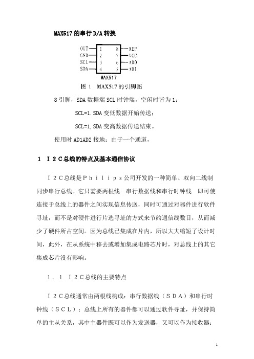
MAX517的串行D/A转换8引脚,SDA数据端SCL时钟端,空闲时皆为1;SCL=1.SDA变低数据开始传送;SCL=1,SDA变高数据传送结束。
使用时AD1AD2接地;由于一个通道,1I2C总线的特点及基本通信协议I2C总线是Philips公司开发的一种简单、双向二线制同步串行总线。
它只需要两根线 串行数据线和串行时钟线即可使连接于总线上的器件之间实现信息传送,同时可通过对器件进行软件寻址,而不是对硬件进行片选寻址的方式来节约通信线数目,从而减少了硬件所占空间。
因为总线已集成在片内,所以大大缩短了设计时间,此外,在从系统中移去或增加集成电路芯片时,对总线上的其它集成芯片没有影响。
1.1I2C总线的主要特点I2C总线通常由两根线构成:串行数据线(SDA)和串行时钟线(SCL);总线上所有的器件都可以通过软件寻址,并保持简单的主从关系,其中主器件既可以作为发送器,又可以作为接收器;I2C总线是一个真正的多主总线,它带有竞争监测和仲裁电路。
当多个主器件同时启动设备时,总线系统会自动进行冲突监测及仲裁,从而确保了数据的正确性;I2C总线采用8位、双向串行数据传送方式,标准传送速率为100kB/s,快速方式下可达400kB/s;同步时钟可以作为停止或重新启动串行口发送的握手方式;连接到同一总线的集成电路数目只受400pF的最大总线电容的限制。
1.2I2C总线数据通信基本协议利用I2C总线进行数据通信时,应遵守如下基本操作:(1)总线应处于不忙状态,当数据总线(SDA)和时钟总线(SCL)都为高电平时,为不忙状态;(2)当SCL为高电平时,SDA电平由高变低时,数据传送开始。
所有的操作必须在开始之后进行;(3)当SCL为高电平时,SDA电平由低变为高时,数据传送结束。
在结束条件下,所有的操作都不能进行;(4)数据的有效转换开始后,当时钟线SCL为高电平时,数据线SDA必须保持稳定。
若数据线SDA改变时,必须在时钟线SCL为低电平时方可进行。

CS5171, CS5172, CS5173, CS51741.5 A 280 kHz/560 kHz Boost RegulatorsThe CS5171/2/3/4 products are 280 kHz/560 kHz switching regulators with a high efficiency, 1.5 A integrated switch. These partsoperate over a wide input voltage range, from 2.7 V to 30 V. The flexibility of the design allows the chips to operate in most power supply configurations, including boost, flyback, forward, inverting, and SEPIC. The ICs utilize current mode architecture, which allows excellent load and line regulation, as well as a practical means for limiting current. Combining high frequency operation with a highly integrated regulator circuit results in an extremely compact power supply solution. The circuit design includes provisions for features such as frequency synchronization, shutdown, and feedback controls for either positive or negative voltage regulation. These parts are pin−to−pin compatible with LT1372/1373.Features•Pb−Free Packages are Available•Integrated Power Switch: 1.5 A Guaranteed•Wide Input Range: 2.7 V to 30 V•High Frequency Allows for Small Components•Minimum External Components•Easy External Synchronization•Built in Overcurrent Protection•Frequency Foldback Reduces Component Stress During an Overcurrent Condition•Thermal Shutdown with Hysteresis•Regulates Either Positive or Negative Output V oltages•Shut Down Current: 50 m A Maximum•Pin−to−Pin Compatible with LT1372/1373•Wide Temperature Range♦Industrial Grade: −40°C to 125°C♦Commercial Grade: 0°C to 125°CORDERING INFORMATIONSee detailed ordering and shipping information in the package dimensions section on page 17 of this data sheet.架构频率同步无铅封装上市5 VSS 3.3 VFigure 1. Applications DiagramMAXIMUM RATINGSvalues (not normal operating conditions) and are not valid simultaneously. If these limits are exceeded, device functional operation is not implied,damage may occur and reliability may be affected.1.60 second maximum above 183°C.MAXIMUM RATINGSELECTRICAL CHARACTERISTICS (2.7 V< V CC < 30 V; Industrial Grade: −40°C < T J < 125°C; Commercial Grade: 0°C < T < 125°C; For all CS5171/2/3/4 specifications unless otherwise stated.)Positive and Negative Error AmplifiersOscillatorSync/ Shutdown2.Guaranteed by design, not 100% tested in production.ELECTRICAL CHARACTERISTICS (continued) (2.7 V< V CC < 30 V; Industrial Grade: −40°C < T J < 125°C;Commercial Grade: 0°C < T< 125°C; For all CS5171/2/3/4 specifications unless otherwise stated.)Power SwitchGeneral3.Guaranteed by design, not 100% tested in production.PACKAGE PIN DESCRIPTIONPGNDV SWCFigure 2. Block DiagramTemperature (°C)Figure 3. I CC (No Switching) vs. Temperature C u r r e n t (m A )Temperature (°C)Figure 4. D I CC / D IV SW vs. Temperature(m A /A )I SW (mA)Figure 5. V CE(SAT) vs. I SWV C E (S A T ) (m V )120010008006004002000Temperature (°C)Figure 6. Minimum Input Voltage vs. TemperatureV I N (V )1.51.61.71.81.9010050Temperature (°C)Figure 7. Switching Frequency vs. Temperature(CS5171/2 only)f O S C (k H z )255260265270275010050280285Temperature (°C)Figure 8. Switching Frequency vs. Temperature(CS5173/4 only)f O S C (k H z )5405455505555600565570535530525520Temperature (°C)V o l t a g e (V )Temperature (°C)Temperature (°C)I F B (m A )0.080.100.120.140.160100500.180.20V CC = 12 VV CC = 2.7 VV FB (mV)f O S C (% o f T y p i c a l )V NFB (mV)f O S C (% o f T y p i c a l )Temperature (°C)I N F B (m A )−7−8−10050−9−11−12−13−14Figure 9. Switching Frequency vs. V FB(CS5171/3 only)Figure 10. Switching Frequency vs. V NFB(CS5172/4 only)Figure 11. Reference Voltage vs. Temperature(CS5171/3 only)Figure 12. Reference Voltage vs. Temperature(CS5172/4 only)Figure 13. I FB vs. Temperature (CS5171/3 only)Figure 14. I NFB vs. Temperature (CS5172/ 4 only)V o l t a g e (V )0.50.60.70.80.91.01.10.4C u r r e n t (A )Temperature (°C)D e l a y (m s )801001201401606040D u t y C y c l e (%)V SS (V)I S S (m A )Temperature (°C)V o l t a g e (V )Figure 17. V C Threshold and High ClampVoltage vs. TemperatureFigure 19. Shutdown Delay vs. TemperatureFigure 20. I SS vs. V SSV IN (V)I C C (m A )V REF − V FB (mV)I O U T (m A )20601000−20−6025−25−75Temperature (°C)g m (m m h o )450500550600V REF − V NFB (mV)I O U T (m A )20601000−20−60−100−150−20080400−40Temperature (°C)g m (m m h o )16017050180190150140130120110100Temperature (°C)C u r r e n t (m A )2.62.52.42.32.22.12.0Figure 21. I CC vs. V IN During ShutdownFigure 22. Error Amplifier Transconductancevs. Temperature (CS5171/3 only)Figure 23. Negative Error AmplifierTransconductance vs. Temperature (CS5172/4 only)Figure 24. Error Amplifier I OUT vs. V FB(CS5171/3 only)Figure 25. Error Amplifier I OUT vs. V NFB(CS5172/4 only)Figure 26. Switch Leakage vs. TemperatureAPPLICATIONS INFORMATIONTHEORY OF OPERATIONCurrent Mode ControlLOADFigure 27. Current Mode Control SchemeThe CS517x family incorporates a current mode control scheme, in which the PWM ramp signal is derived from the power switch current. This ramp signal is compared to the output of the error amplifier to control the on−time of the power switch. The oscillator is used as a fixed−frequency clock to ensure a constant operational frequency. The resulting control scheme features several advantages over conventional voltage mode control. First, derived directly from the inductor, the ramp signal responds immediately to line voltage changes. This eliminates the delay caused by the output filter and error amplifier, which is commonly found in voltage mode controllers. The second benefit comes from inherent pulse−by−pulse current limiting by merely clamping the peak switching current. Finally, since current mode commands an output current rather than voltage, the filter offers only a single pole to the feedback loop. This allows both a simpler compensation and a higher gain−bandwidth over a comparable voltage mode circuit.Without discrediting its apparent merits, current mode control comes with its own peculiar problems, mainly,subharmonic oscillation at duty cycles over 50%. The CS517x family solves this problem by adopting a slope compensation scheme in which a fixed ramp generated by the oscillator is added to the current ramp. A proper slope rate is provided to improve circuit stability without sacrificing the advantages of current mode control.Oscillator and ShutdownFigure 28. Timing Diagram of Sync and ShutdownV SWCurrent Ramp Sync The oscillator is trimmed to guarantee an 18% frequency accuracy. The output of the oscillator turns on the power switch at a frequency of 280 kHz (CS5171/2) or 560 kHz (CS5173/4), as shown in Figure 27. The power switch is turned off by the output of the PWM Comparator.A TTL−compatible sync input at the SS pin is capable of syncing up to 1.8 times the base oscillator frequency. As shown in Figure 28, in order to sync to a higher frequency,a positive transition turns on the power switch before the output of the oscillator goes high, thereby resetting the oscillator. The sync operation allows multiple power supplies to operate at the same frequency.A sustained logic low at the SS pin will shut down the IC and reduce the supply current.An additional feature includes frequency shift to 20% of the nominal frequency when either the NFB or FB pins trigger the threshold. During power up, overload, or short circuit conditions, the minimum switch on−time is limited by the PWM comparator minimum pulse width. Extra switch off−time reduces the minimum duty cycle to protect external components and the IC itself.As previously mentioned, this block also produces a ramp for the slope compensation to improve regulator stability.Error AmplifierFigure 29. Error Amplifier Equivalent CircuitFBNFBWm F For CS5172/4, the NFB pin is internally referenced to −2.5 V with approximately a 250 k W input impedance. For CS5171/3, the FB pin is directly connected to the inverting input of the positive error amplifier, whose non−inverting input is fed by the 1.276 V reference. Both amplifiers are transconductance amplifiers with a high output impedance of approximately 1 M W , as shown in Figure 29. The V C pin is connected to the output of the error amplifiers and is internally clamped between 0.5 V and 1.7 V . A typical connection at the V C pin includes a capacitor in series with a resistor to ground, forming a pole/zero for loop compensation.An external shunt can be connected between the V C pin and ground to reduce its clamp voltage. Consequently, the current limit of the internal power transistor current is reduced from its nominal value.Switch Driver and Power SwitchThe switch driver receives a control signal from the logic section to drive the output power switch. The switch is grounded through emitter resistors (63 m W total) to the PGND pin. PGND is not connected to the IC substrate so that switching noise can be isolated from the analog ground. The peak switching current is clamped by an internal circuit. The clamp current is guaranteed to be greater than 1.5 A and varies with duty cycle due to slope compensation. The power switch can withstand a maximum voltage of 40 V on the collector (V SW pin). The saturation voltage of the switch is typically less than 1 V to minimize power dissipation.Short Circuit ConditionWhen a short circuit condition happens in a boost circuit,the inductor current will increase during the whole switching cycle, causing excessive current to be drawn from the input power supply. Since control ICs don’t have the means to limit load current, an external current limit circuit (such as a fuse or relay) has to be implemented to protect the load, power supply and ICs.In other topologies, the frequency shift built into the IC prevents damage to the chip and external components. This feature reduces the minimum duty cycle and allows the transformer secondary to absorb excess energy before the switch turns back on.Figure 30. Startup Waveforms of Circuit Shown inthe Application Diagram. Load = 400 mA.I LV OUT V CV CCThe CS517x can be activated by either connecting the V CC pin to a voltage source or by enabling the SS pin.Startup waveforms shown in Figure 30 are measured in the boost converter demonstrated in the Application Diagram on the page 2 of this document. Recorded after the input voltage is turned on, this waveform shows the various phases during the power up transition.When the V CC voltage is below the minimum supply voltage, the V SW pin is in high impedance. Therefore,current conducts directly from the input power source to the output through the inductor and diode. Once V CC reachesapproximately 1.5 V , the internal power switch briefly turns on. This is a part of the CS517x’s normal operation. The turn−on of the power switch accounts for the initial current swing.When the V C pin voltage rises above the threshold, the internal power switch starts to switch and a voltage pulse can be seen at the V SW pin. Detecting a low output voltage at the FB pin, the built−in frequency shift feature reduces the switching frequency to a fraction of its nominal value,reducing the minimum duty cycle, which is otherwise limited by the minimum on−time of the switch. The peak current during this phase is clamped by the internal current limit.When the FB pin voltage rises above 0.4 V , the frequency increases to its nominal value, and the peak current begins to decrease as the output approaches the regulation voltage.The overshoot of the output voltage is prevented by the active pull−on, by which the sink current of the error amplifier is increased once an overvoltage condition is detected. The overvoltage condition is defined as when the FB pin voltage is 50 mV greater than the reference PONENT SELECTIONFrequency CompensationThe goal of frequency compensation is to achieve desirable transient response and DC regulation while ensuring the stability of the system. A typical compensation network, as shown in Figure 31, provides a frequency response of two poles and one zero. This frequency response is further illustrated in the Bode plot shown in Figure 32.Figure 31. A Typical Compensation NetworkC2The high DC gain in Figure 32 is desirable for achieving DC accuracy over line and load variations. The DC gain of a transconductance error amplifier can be calculated as follows:Gain DC +G M R Owhere:G M = error amplifier transconductance;R O = error amplifier output resistance ≈ 1 M W .The low frequency pole, f P1, is determined by the error amplifier output resistance and C1 as:f P1+1OThe first zero generated by C1 and R1 is:f Z1+1The phase lead provided by this zero ensures that the loop has at least a 45° phase margin at the crossover frequency.Therefore, this zero should be placed close to the pole generated in the power stage which can be identified at frequency:f P +12p C O R LOADwhere:C O = equivalent output capacitance of the error amplifier ≈120pF;R LOAD = load resistance.The high frequency pole, f P2, can be placed at the output filter’s ESR zero or at half the switching frequency. Placing the pole at this frequency will cut down on switching noise.The frequency of this pole is determined by the value of C2and R1:f P2+12p C2R1One simple method to ensure adequate phase margin is todesign the frequency response with a −20 dB per decade slope, until unity−gain crossover. The crossover frequency should be selected at the midpoint between f Z1 and f P2 wherethe phase margin is maximized.Figure 32. Bode Plot of the Compensation NetworkShown in Figure 31Frequency (LOG)G a i n (d B )Negative Voltage FeedbackSince the negative error amplifier has finite input impedance as shown in Figure 33, its induced error has to be considered. If a voltage divider is used to scale down the negative output voltage for the NFB pin, the equation for calculating output voltage is:*V OUT +ǒ*2.5(R1)R2)R2Ǔ*10m A R1Figure 33. Negative Error Amplifier and NFB PinIt is shown that if R1 is less than 10 k, the deviation from the design target will be less than 0.1 V . If the tolerances of the negative voltage reference and NFB pin input current are considered, the possible offset of the output V OFFSET varies in the range of:ǒ*0.0.5(R1)R2)R2Ǔ*(15m A R1)v V OFFSETv ǒ0.0.5(R1)R2)Ǔ*(5m A R1)V SW Voltage LimitIn the boost topology, V SW pin maximum voltage is set by the maximum output voltage plus the output diode forward voltage. The diode forward voltage is typically 0.5 V for Schottky diodes and 0.8 V for ultrafast recovery diodesV SW(MAX)+V OUT(MAX))V Fwhere:V F = output diode forward voltage.In the flyback topology, peak V SW voltage is governed by:V SW(MAX)+V CC(MAX))(V OUT )V F ) Nwhere:N = transformer turns ratio, primary over secondary.When the power switch turns off, there exists a voltage spike superimposed on top of the steady−state ually this voltage spike is caused by transformer leakage inductance charging stray capacitance between the V SW and PGND pins. To prevent the voltage at the V SW pin from exceeding the maximum rating, a transient voltage suppressor in series with a diode is paralleled with the primary windings. Another method of clamping switch voltage is to connect a transient voltage suppressor between the V SW pin and ground.Magnetic Component SelectionWhen choosing a magnetic component, one must consider factors such as peak current, core and ferrite material, output voltage ripple, EMI, temperature range, physical size and cost. In boost circuits, the average inductor current is the product of output current and voltage gain (V OUT /V CC ),assuming 100% energy transfer efficiency. In continuous conduction mode, inductor ripple current isI RIPPLE +V CC (V OUT*V CC )OUT)where:f = 280 kHz for CS5171/2 and 560 kHz for CS5173/4.The peak inductor current is equal to average current plus half of the ripple current, which should not cause inductor saturation. The above equation can also be referenced when selecting the value of the inductor based on the tolerance of the ripple current in the circuits. Small ripple current provides the benefits of small input capacitors and greater output current capability. A core geometry like a rod or barrel is prone to generating high magnetic field radiation,but is relatively cheap and small. Other core geometries,such as toroids, provide a closed magnetic loop to prevent EMI.Input Capacitor SelectionIn boost circuits, the inductor becomes part of the input filter, as shown in Figure 35. In continuous mode, the input current waveform is triangular and does not contain a large pulsed current, as shown in Figure 34. This reduces the requirements imposed on the input capacitor selection.During continuous conduction mode, the peak to peak inductor ripple current is given in the previous section. As we can see from Figure 34, the product of the inductor current ripple and the input capacitor’s effective series resistance (ESR) determine the V CC ripple. In most applications, input capacitors in the range of 10 m F to 100 m F with an ESR less than 0.3 W work well up to a full 1.5 A switch current.V CC rippleFigure 34. Boost Input Voltage and CurrentRipple WaveformsI INI LFigure 35. Boost Circuit Effective Input FilterV CCI The situation is different in a flyback circuit. The input current is discontinuous and a significant pulsed current is seen by the input capacitors. Therefore, there are two requirements for capacitors in a flyback regulator: energy storage and filtering. To maintain a stable voltage supply to the chip, a storage capacitor larger than 20 m F with low ESR is required. To reduce the noise generated by the inductor,insert a 1.0 m F ceramic capacitor between V CC and ground as close as possible to the chip.Output Capacitor SelectionFigure 36. Typical Output Voltage RippleV OUT rippleI LBy examining the waveforms shown in Figure 36, we can see that the output voltage ripple comes from two major sources, namely capacitor ESR and the charging/discharging of the output capacitor. In boost circuits, when the power switch turns off, I L flows into the output capacitor causing an instant D V = I IN × ESR. At the same time, current I L − I OUT charges the capacitor and increases the output voltage gradually. When the power switch is turned on, I L is shunted to ground and I OUT discharges the output capacitor. When the I L ripple is small enough, I L can be treated as a constant and is equal to input current I IN .Summing up, the output voltage peak−peak ripple can be calculated by:V OUT(RIPPLE)+(I IN*I OUT)(1*D)(C OUT)(f))I OUT DOUT)I IN ESRThe equation can be expressed more conveniently in terms of V CC, V OUT and I OUT for design purposes as follows:V OUT(RIPPLE)+I OUT(V OUT*V CC)(C OUT)(f)1(C OUT)(f))(I OUT)(V OUT)(ESR)V CCThe capacitor RMS ripple current is:I RIPPLE+(I IN*I OUT)2(1*D))(I OUT)2(D)Ǹ+I OUT V OUT *V CCV CCǸAlthough the above equations apply only for boost circuits, similar equations can be derived for flyback circuits.Reducing the Current LimitIn some applications, the designer may prefer a lower limit on the switch current than 1.5 A. An external shunt can be connected between the V C pin and ground to reduce its clamp voltage. Consequently, the current limit of the internal power transistor current is reduced from its nominal value.The voltage on the V C pin can be evaluated with the equationV C+I SW R E A Vwhere:R E = .063W, the value of the internal emitter resistor;A V = 5 V/V, the gain of the current sense amplifier. Since R E and A V cannot be changed by the end user, the only available method for limiting switch current below 1.5 A is to clamp the V C pin at a lower voltage. If the maximum switch or inductor current is substituted into the equation above, the desired clamp voltage will result.A simple diode clamp, as shown in Figure 37, clamps the V C voltage to a diode drop above the voltage on resistor R3.Unfortunately, such a simple circuit is not generally acceptable if V INis loosely regulated.Figure 37. Current Limiting using a Diode Clamp V INAnother solution to the current limiting problem is to externally measure the current through the switch using a sense resistor. Such a circuit is illustrated in Figure 38.Figure 38. Current Limiting using a Current SenseResistorVOutputGround The switch current is limited toI SWITCH(PEAK)+V BE(Q1)SENSEwhere:V BE(Q1) = the base−emitter voltage drop of Q1, typically 0.65 V.The improved circuit does not require a regulated voltage to operate properly. Unfortunately, a price must be paid for this convenience in the overall efficiency of the circuit. The designer should note that the input and output grounds are no longer common. Also, the addition of the current sense resistor, R SENSE , results in a considerable power loss which increases with the duty cycle. Resistor R2 and capacitor C3form a low−pass filter to remove noise.Subharmonic OscillationSubharmonic oscillation (SHM) is a problem found in current−mode control systems, where instability results when duty cycle exceeds 50%. SHM only occurs in switching regulators with a continuous inductor current.This instability is not harmful to the converter and usually does not affect the output voltage regulation. SHM will increase the radiated EM noise from the converter and can cause, under certain circumstances, the inductor to emit high−frequency audible noise.SHM is an easily remedied problem. The rising slope of the inductor current is supplemented with internal “slope compensation” to prevent any duty cycle instability from carrying through to the next switching cycle. In the CS517x family, slope compensation is added during the entire switch on−time, typically in the amount of 180 mA/m s.In some cases, SHM can rear its ugly head despite the presence of the onboard slope compensation. The simple cure to this problem is more slope compensation to avoid the unwanted oscillation. In that case, an external circuit, shown in Figure 39, can be added to increase the amount of slope compensation used. This circuit requires only a few components and is “tacked on” to the compensationnetwork.Figure 39. Technique for Increasing SlopeCompensationSWThe dashed box contains the normal compensation circuitry to limit the bandwidth of the error amplifier.Resistors R2 and R3 form a voltage divider off of the V SW pin. In normal operation, V SW looks similar to a square wave, and is dependent on the converter topology. Formulas for calculating V SW in the boost and flyback topologies are given in the section “V SW V oltage Limit.” The voltage on V SW charges capacitor C3 when the switch is off, causing the voltage at the V C pin to shift upwards. When the switch turns on, C3 discharges through R3, producing a negative slope at the V C pin. This negative slope provides the slope compensation.The amount of slope compensation added by this circuit isD I D T+VSW ǒR 3R 2)R 3Ǔǒ1*e*(1*D)R 3C 3f SW Ǔǒf SW (1*D)R E A VǓwhere:D I/D T = the amount of slope compensation added (A/s);V SW = the voltage at the switch node when the transistor is turned off (V);f SW = the switching frequency, typically 280 kHz (CS5171/3) or 560 kHz (CS5172/4) (Hz);D = the duty cycle;R E = 0.063 W , the value of the internal emitter resistor;A V = 5 V/V , the gain of the current sense amplifier.In selecting appropriate values for the slope compensation network, the designer is advised to choose a convenient capacitor, then select values for R2 and R3 such that the amount of slope compensation added is 100 mA/m s. Then R2 may be increased or decreased as necessary. Of course,the series combination of R2 and R3 should be large enough to avoid drawing excessive current from V SW . Additionally,to ensure that the control loop stability is improved , the time constant formed by the additional components should be chosen such thatR 3C 3t 1*Df SWFinally, it is worth mentioning that the added slope compensation is a tradeoff between duty cycle stability and transient response. The more slope compensation a designer adds, the slower the transient response will be, due to the external circuitry interfering with the proper operation of the error amplifier.Soft−StartThrough the addition of an external circuit, a Soft−Start function can be added to the CS5171/2/3/4 family of components. Soft−Start circuitry prevents the V C pin from slamming high during startup, thereby inhibiting the inductor current from rising at a high slope.This circuit, shown in Figure 40, requires a minimum number of components and allows the Soft−Start circuitry toactivate any time the SS pin is used to restart the converter.Figure 40. Soft StartV INSSResistor R1 and capacitors C1 and C2 form the compensation network. At turn on, the voltage at the V C pin starts to come up, charging capacitor C3 through Schottky diode D2, clamping the voltage at the V C pin such that switching begins when V C reaches the V C threshold,typically 1.05 V (refer to graphs for detail over temperature).V C +V F(D2))V C3Therefore, C3 slows the startup of the circuit by limiting the voltage on the V C pin. The Soft−Start time increases with the size of C3.Diode D1 discharges C3 when SS is low. If the shutdown function is not used with this part, the cathode of D1 should be connected to V IN .Calculating Junction TemperatureTo ensure safe operation of the CS5171/2/3/4, the designer must calculate the on−chip power dissipation and determine its expected junction temperature. Internal thermal protection circuitry will turn the part off once the junction temperature exceeds 180°C ±30°. However,repeated operation at such high temperatures will ensure a reduced operating life.Calculation of the junction temperature is an imprecise but simple task. First, the power losses must be quantified.There are three major sources of power loss on the CS517x:•biasing of internal control circuitry, P BIAS •switch driver, P DRIVER •switch saturation, P SATThe internal control circuitry, including the oscillator and linear regulator, requires a small amount of power evenwhen the switch is turned off. The specifications section of this datasheet reveals that the typical operating current, I Q ,due to this circuitry is 5.5 mA. Additional guidance can be found in the graph of operating current vs. temperature. This graph shows that IQ is strongly dependent on input voltage,V IN , and temperature. ThenP BIAS +V IN I QSince the onboard switch is an NPN transistor, the base drive current must be factored in as well. This current is drawn from the V IN pin, in addition to the control circuitry current. The base drive current is listed in the specifications as D I CC /D I SW , or switch transconductance. As before, the designer will find additional guidance in the graphs. With that information, the designer can calculateP DRIVER +V IN I SW ICC D I SWDwhere:I SW = the current through the switch;D = the duty cycle or percentage of switch on−time.I SW and D are dependent on the type of converter. In a boost converter,I SW(AVG)^I LOAD D1EfficiencyD ^V OUT*V IN V OUTIn a flyback converter,I SW(AVG)^V OUT I LOAD V IN1Efficiency D ^V OUT V OUT )NSN P V INThe switch saturation voltage, V (CE)SAT , is the last major source of on−chip power loss. V (CE)SAT is the collector−emitter voltage of the internal NPN transistor when it is driven into saturation by its base drive current. The value for V (CE)SAT can be obtained from the specifications or from the graphs, as “Switch Saturation V oltage.” Thus,P SAT ^V (CE)SAT I SW DFinally, the total on−chip power losses areP D +P BIAS )P DRIVER )P SATPower dissipation in a semiconductor device results in the generation of heat in the junctions at the surface of the chip.This heat is transferred to the surface of the IC package, but a thermal gradient exists due to the resistive properties of the package molding compound. The magnitude of the thermal gradient is expressed in manufacturers’ data sheets as q JA ,or junction−to−ambient thermal resistance. The on−chip junction temperature can be calculated if q JA , the air temperature near the surface of the IC, and the on−chip power dissipation are known.。
高性能LNB 专用控制芯片FD9515器件手册(中文版本)版本:B2_CN 日期:2014-01-26F DHI S I CON F IDE N T I A L著作权Copyright © 2013 by FUZHOU FUDA HISI MICROELECTRONICS CO.,LTD. 使用指南中所出现的信息在出版当时相信是正确的,然而福大海矽对于说明书的使用不负任何责任。
文中提到的应用目的仅仅是用来做说明,福大海矽不保证或表示这些没有进一步修改的应用将是适当的,也不推荐它的产品使用在会由于故障或其它原因可能会对人身造成危害的地方。
福大海矽产品不授权使用于救生、维生器件或系统中做为关键器件。
福大海矽拥有不事先通知而修改产品的权利,对于最新的信息,请参考我们的网址版本修订记录联系方式福州福大海矽微电子有限公司地址:中国,福建省,福州市鼓楼区工业路523号福州大学物理北楼四层邮编: 350002传真: *************电话: *************F DHI S DE N T I A L目录一、 概述 ............................................................................................................. 1 二、 特性说明 ...................................................................................................... 1 三、 应用领域 ...................................................................................................... 1 四、 管脚定义(SOP8EP ) ................................................................................. 2 五、 管脚功能说明 ............................................................................................... 2 六、 产品基本信息 ............................................................................................... 3 七、 主要电气参数 ............................................................................................... 3 八、 典型电路 ...................................................................................................... 6 九、 功能描述 ...................................................................................................... 7 十、 D I SE Q C 信号整形 ........................................................................................ 8 十一、线性稳压电路 (8)十二、 短路及过载保护 ..................................................................................... 8 十三、 控制信号整形 ......................................................................................... 8 十四、 LNB 22K 控制波形图解 .......................................................................... 8 十五、 参考测试波形 ......................................................................................... 9 十六、封装尺寸图(SOP8EP ) (12)F DHI S I CON F IDE N T I A L高性能LNB 专用控制芯片FD9515一、 概述FD9515为业内首颗高性能SOP8封装的LNB 专用控制集成电路,该芯片提供卫星电视接收机LNB 控制应用的完整功能,符合欧洲一流运营商及NorDig 标准要求,并根据实际应用经验及需求,优化各项性能指标,最小化外围BOM 成本。