KMS9412实现同步升压输出5V2A,输入5v2.1A移动电源单芯片方案
- 格式:pdf
- 大小:648.12 KB
- 文档页数:6


_______________________________________________________XySemi Inc - 1 - S5802-SIP of Power Bank Total Solution GENERAL DESCRIPTIONS5802 is one SIP that it integrates Li-Battery Charge management 、Li-BatteryProtection and Boost converter in only TSSOP16-PP package.This SIP can charge with 1A current and also can output 5V 1A to load such as smart phone or MID.It only need few components and can reduce the BOM area and BOM cost.FEATURESz Charger input voltage-4.5V to 6V z Charger current-MAX 1Az Boost converter-MAX 20V output z Boost converter-MAX 5V 1Az Boost converter Frequency-1.2MHz z Li Protection OCU-4.25V ODU-2.9V z Li Protection OCP-3A z Have UVLO 、OTP 、Short protection z TSSOP16-PP PackageAPPLICATIONS• Power bank for MID 、PAD •Power bank for Smart PhoneFigure 1. Typical Application Circuit1____________________________________________________________________________________________________ORDERING INFORMATIONPART NUMBER TEMP RANGE VIN OUTPUT VOLTAGE (V)CHARGE CURRENTPACKAGE PINS S5802-40°C to 85°C4.5~6VADJ1ATSSOP-PP 16PIN CONFIGURATIONFigure 2. PIN ConfigurationPIN DESCRIPTIONPIN NUMBER PIN NAME PIN DESCRIPTION1,2SWBoost Converter’s Switching pin3,12 B+Li-Battery’s Positive Pole ,pin 3 should be bypassed with a 1uF capacitor as close aspossible, Pin12 should be bypassed with a 10uF capacitor as close as possible 4 BSOCBoost Converter’s current limit setting pin ,For 5Vout 1A application ,you can select250K~300Kohm resistor to GND 5 BSEN Boost Converter’s Enable pin 6FBBoost Converter’s Feedback pin. it can set 5Vout with two resistors.7 CHRG Open-Drain Charge Status Output , When the battery is charging, the CHRG pin ispulled low by an internal N-channel MOSFET. When the charge cycle is completed,CHRG pin will be in a high-impedance state. 8 CHEN Charge Enable Pin9PROG Charge Current Program, Charge Current Monitor and Shutdown Pin.10 CHSTD The completion of battery charging instructions side. When the battery charge iscomplete, CHSTD pulled low by internal switches, indicating the completion ofcharging. In addition, CHSTD pin will be in a high-impedance state. 11CHINPositive Input Supply Voltage, should be bypassed with at least a 10uF capacitor.S5802____________________________________________________________________________________________________13 VPBThe Power Supply of Li-Protection section ,Should connect 0.1uF capacitor betweenVpb and B- as close as possible and 100ohm resistor to B+ 14,15 B- Li-Battery’s Negative Pole 16,17GNDGround and EPADABSOLUTE MAXIMUM RATINGS(Note: Do not exceed these limits to prevent damage to the device. Exposure to absolute maximum rating conditions for long periods may affect device reliability.)PARAMETER VALUE UNITSupply Voltage VIN ;CHRG\CHEN\CHSTD Voltage -0.3 to 7 V FB Voltage ;Vpb Voltage ;B+\B-; BSEN pin; BSOC voltage -0.3 to 5 V SW Voltage Vin+0.3 to 15 V PROG Voltage-0.3~CHIN+0.3V Icharge 1.2 APROG Pin current1.2 mA Operating Ambient Temperature -40 to 85 °C Maximum Junction Temperature 150 °C Storage Temperature-55 to 150 °C Lead Temperature (Soldering, 10 sec)260°CELECTRICAL CHARACTERISTICS(V IN = 3.6V, T A = 25°C unless otherwise specified)PARAMETER SYMBOL TEST CONDITIONSMIN TYP MAX UNITInput Voltage Range CHIN 4.5 6.0V Regulated Charge Voltage Vfloat0°C ≤T A ≤85°C, Icharge = 40mA4.158 4.2 4.242V PROG pin Voltage Vprog R PROG =1k, Current mode0.93 1.0 1.07V R PROG =2k,Current mode450 500 550mA R PROG =1k,Current mode900 1000 1100mA Charge current Icharge Standby mode,Vbat=4.2V0 -2.5 -6 uA Trickle charge current Itrikl Vbat<Vtrikl,Rprog=1k 90100110mA Trickle charge Threshold VoltageVtriklR PROG =10K ,Vbat Rising2.8 2.93.0V Trickle voltage hysteresis voltageVtrhys R PROG =10K 6080110mV CHRG pin Output low voltageVchrg Ichrg =5mA 0.35 0.6V CHSTD pin Output low voltageVchstd Ichstd =5mA0.35 0.6VFUNCTIONAL DESCRIPTIONNORMAL OPERATIONS5802 integrates Li-Battery Charger 、Li-Battery Protection and Boost converter in only TSSOP16-PP packageAdapter inputs 5V voltage and charges the battery. After the battery is full, get off the adapter . And then we can boost up to 5V to charge the mobile advices when they is empty.Li-Battery Charger can set charge current by PROG resistor. Normal charging current is set from 0.5A to 1A. It will go into trickle charge mode to protect Li-Battery when BAT voltage is below 2.9V. Li-Battery Protection can detect the battery cell’s status such as Vcu 、Vcl ,Temp 、short-cut 、Over-current and take action to protect battery cell.Boost section can give us 5V 1A capacity to mobile devices.THERMAL OR SHORT-CUT PROTECTIONA thermal shutdown is implemented to prevent damages due to excessive heat and power dissipation. Typically the thermal shutdown threshold is 150℃ .When the thermal shutdown is triggered the device stops switching until the temperature falls below typically 136℃.Then the device starts switching again.If the Boost converter’s Vout is short to GND ,the IC will shut down and you should recharge the battery to get rid of this status.CHEN 、BSEN voltage Ven0.3 1 1.5VRecharge Battery threshold VoltageΔVrecg V FLOAT - V RECHRG 100 200mV Overcharge DetectionVoltage of Li BAT-Protection V CU 4.225 4.25 4.275V Overcharge Release Voltage of Li BAT-Protection V CL 4.075 4.10 4.125V Overdischarge DetectionVoltage of Li BAT-Protection V DL 2.85 2.9 2.95VOverdischarge ReleaseVoltage of Li BAT-Protection V DR2.953.0 3.05VOverdischarge Current1 Detection of Li BAT-ProtectionI IOV1 (V B+)-(V B -)=3.5V 2.1 3 3.9 ALoad Short-Circuiting Detection of Li BAT-ProtectionI SHORT (V B+)-(V B -)=3.5V 10 20 30 ABoost output voltage range Vout 20 VRegulated Feedback Voltage V FB1.118 1.2 1.212VPeak Inductor Current I PEAK Rset=150K Vin=3.3V Vout=5V 0.8 1 1.2 A Peak Inductor Current I PEAK Rset=500K Vin=3.3V Vout=5V2.2 2.55 2.9ABoost ConvertOscillator FrequencyF OSC0.9 1.2 1.5MHzAPPLICATION INFORMATIONINDUCTOR SELECTIONIn normal operation, the inductor maintains continuous current to the output. The inductor current has a ripple that is dependent on the inductance value. The high inductance reduces the ripple current.Selected inductor by actual application:Manufa cturer Part Number Inductance (uH) DRC max(Ohms)Dimensions L*W*H(mm3)2.2 0.0493.3 0.0654.7 0.08 LQH44PN10 0.164*4*1.7 2.2 0.0303.3 0.0444.7 0.058 MurataLQH5BP10 0.1065*5*2 2.2 0017 3.3 0.027 TDK SPM6530T4.7 0.0367.1*6.5*3 744373 240222.2 0.0614.4*4.05WURTH 744777004 4.70.0257.3*7.3*4.5Table 1. Recommend Surface Mount InductorsIf output voltage is 5V ,you can use 2.2uH~ 4.7uH, If output voltage is 12V, 4.7uH~ 10uH is OK , Normal application: Input 3.3V (3.6V or 4.2V) to Output 5V 9V 12V ;Input 5V to Output 9V 12VCAPACITOR SELECTIONThe input capacitor reduces input voltage ripple to the converter, low ESR ceramic capacitor is highly recommended. For power bank application, A 10uF ceramic capacitor is used. The input capacitor should be placed as close as possible to CHIN and GND. Such as Murata GRM21BR60J106 or TDK C3216X5R1A106M A low ESR output capacitor is required in order to maintain low output voltage ripple. one 10~22uF ceramic output capacitor is suitable for most applications. Such as GRM21BR60J226 or TDK C3216X5R1A226M B+-Pin 3 should be bypassed with a 1uF capacitor as close as possible , B+-Pin12 should be bypassed with a 10uF capacitor as close as possible.SET CHARGE CURRENTThe charge current is programmed by connecting a 1% resistor, R PROG , PROG pin to ground. When charging in constant-current mode, this pin servos to 1V. In all modes, the voltage on this pin can be used to measure the charge current using the following formula: I charge = (V PROG /R PROG ) •1000.OUTPUT VOLTAGE PROGRAMMINGThe output voltage is set by a resistive divider according to the following equation:Typically choose R2=30K and determine R1 from the following equation:For example, you can select R2=31.5K R1=100K to set 5VoutDIODE SELECTIONAccording to max Iout and max Vout, you can select suitable diode. Normally we select diode If=(1.5~2)*Ioutmax and VR=(1.5~2)*Voutmax. For high efficiency,suggest that you select low Vf Schottky diode.For example, 5V 1Aout power bank application, you can select MBRA210LT3 or SS24. Using MBRA210LT3, you can get higher efficiency.OC SETTING( SETTING CURRENT LIMIT)S5802 can be adjusted SW current limit by one resistor connected with BSOC pin。

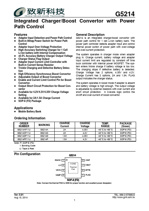
Integrated Charger/Boost Convertor with Power Path ControlFeaturesAdaptor Input Detection and Power Path Control Built-in 90m Ω Power Switch for Power Path ControlAdapter Input Over-Voltage ProtectionHigh Accuracy Switching Charger for 1 Cell Li-lon battery with Internal Compensation±0.5% Accuracy Battery Charger Output Voltage Charger Status Flag OutputAdapter Input Current Limit Controller with Built-in Current Sense ResistorTrickle Charging and Defective Battery Detec-tionHigh Efficiency Synchronous Boost Convertor Adjustable Output of Boost ConvertorEnable and Current Limit Control Pin for Boost Convertor.Output Short Circuit Protection for Boost Con-vertorAvailable for 4.2V/4.3V/4.35V Charge Voltage SettingAvailable for 2A/1.5A Charge CurrentSOP-8 (FD) PackageApplicationsMobile Battery BankGeneral DescriptionG5214 is an integrated charger/boost convertor with power path control for 1 cell Li-lon battery bank. The power path controller detects adapter input and control internal power switch of power path with over-voltage and over-current protection.The system operates in charger mode when adapter plug in. Charge current, battery voltage and adapter input current limit are regulated by constant off time buck controller with internal power MOSFET. The sys-tem enters trickle charge if battery voltage is too low. The charging stops if defective battery is detected. Charge Voltage has 2 options, 4.35V and 4.2V. Charge Current has 2 options, 2A and 1.5A. FLAG output indicates the charger status.The system operates in boost mode if adapter is absent and battery voltage is high enough. The output voltage is adjustable by external resistors with over current and short circuit protection. A 3-levels logic control the on/off and over-current of boost convertor.Ordering InformationORDER NUMBERMARKINGCHARGE CurrentCHARGE Voltage TEMP. RANGE PACKAGE (Green)G5214AF11U G5214A 2A 4.35V -40°C to +85°C SOP-8 (FD) G5214CF11U G5214C 2A 4.2V -40°C to +85°C SOP-8 (FD) G5214DF11U G5214D 1.5A 4.35V -40°C to +85°C SOP-8(FD) G5214FF11U G5214F 1.5A4.2V -40°C to +85°C SOP-8 (FD)Note: F1:SOP-8 (FD) 1: Bonding CodeU: Tape & ReelPin ConfigurationVADPVSYS EN/OCLX CSIP SOP-8 (FD)VBAT FLAGBTFB Note: Connect the thermal PAD to GND for proper function and excellent power dissipationAbsolute Maximum RatingsSupply Voltage (ADP to GND) . . . . . . . . .-0.3V to 6.5V Supply Voltage (ADP to GND, <30µS pulse ). . . . . . . . . . . . . . . . . . . . . . . . . . . . . . . . . . .-0.3V to 9V Supply Voltage (VSYS, VBAT to GND) . . . -0.3V to 6V CSIP to GND . . . . . . . . . . . . . . . . . . . . -0.3V to 6V LX to GND . . . . . . . . . . . . . . . . . . -0.5V to VSYS+0.5V Other Pins to GND. . . . . . . . . . . . . . . . . . . .-0.3V to 6V Thermal Resistance Junction to Ambient, (θJA )SOP-8 (FD) . . . . . . . . . . . . . . . . . . . . . . .132°C/W (1) SOP-8 (FD) (1in 2). . . . . . . . . . . . . . . . . . . . 108°C/W (2) Continuous Power Dissipation (T A = +25°C)SOP-8 (FD) . . . . . . . . . . . . . . . . . . . . . . .0.9W (1) SOP-8 (FD) (1in 2). . . . . . . . . . . . . . . . . . . . . . .1.2W (2) Thermal Resistance Junction to Case, (θJC )SOP-8 (FD) . . . . . . . . . . . . . . . . . . . . . . . . . . . 12°C/WStorage Temperature . . . . . . . . . . . . -65°C to +150°C Junction Temperature . . . . . . . . . . . . -10°C to +150°C Reflow Temperature (soldering, 10sec) . . . . . . .260°C ESD Protection (Human Body Mode) . . . . . . . . . . .2kVRecommended Operation ConditionsSupply Voltage (ADP to GND) . . . . . . . 4.8V to 5.5V Supply Voltage (VBAT to GND) . . . . . . .3V to 4.2V Operation Temperature (T A ) . . . . . . . -40°C to +85°CStress beyond those listed under “Absolute Maximum Ratings ” may cause permanent damage to the device.Note: (1): Please refer to Minimum Footprint PCB Layout Section. (2): Please refer to 1in 2 of 1oz PCB Layout Section.Electrical CharacteristicsADP =5V, V BAT =3.7V, T A =25°C, unless otherwise noted.The device is not guaranteed to function outside its operating conditions. Parameters with MIN and/or MAX limits are 100% tested at +25°C, unless otherwise specified.PARAMETER CONDITION MIN TYP MAX UNITSBattery Quiescent Current I VSYS =0 --- 500 700 µAVBAT=2.5V, Boost Convertor Stops --- 20 30 Battery Leakage CurrentVBAT=3.7V, Pull EN/OC low to shutdown--- 35 45 µAVBAT Rising2.62.752.9VBAT UVLO/ Trickle Charge ThresholdVBAT Falling 2.5 2.65 2.8VSwitch from VADP to VSYS --- 90 100m Ω Switch from VSYS to LX, V SYS =5V ---44 52 m Ω On-Resistance of Switches Switch from LX to GND, V SYS =5V --- 39 45 m Ω VSYS Short Circuit Blanking Time263443msVSYS Short Circuit Auto-Restart Time 177 238 300 msEN/OC input high threshold 4.5 --- ---EN/OC input low threshold --- --- 0.3 EN/OC Threshold EN/OC floating logic threshold 1.1 --- 3 V FLAG On Resistance ADP=5V---18 40 Ω FLAG Pin LeakageFLAG=6V--- 0.1 0.5 µA Thermal Shutdown Threshold Temperature Rising --- 150 --- °C Thermal Shutdown Hysteresis---25---°CAdapter Power Path Control ADP rising 4.65 4.74 4.83 V Adapter Power Good Threshold ADP falling 4.47 4.56 4.64 V ADP rising5.856.02 6.2 V Adapter OVP Threshold ADP falling 5.65 5.78 5.93 V G5214A/B/C, VSYS =0V 2.3 2.6 3.1Current Limit of Power SwitchG5214D/E/F, VSYS =0V1.82.1 2.6AElectrical Characteristics (continued)PARAMETER CONDITIONMINTYPMAX UNITSBOOST CONVERTORBTFB Output Voltage VBAT=3.0V~4.2V, I VSYS=0~2A 0.59 0.61 0.63VVSYS Short Current Limit VBAT>VSYS, R SNS=10mΩ, EN/OC floating 2.1 2.5 2.7 AReduction VSYS Short Current Limit VBAT>VSYS, R SNS=10mΩ, EN/OC input high 1.4 1.69 1.83 AVBAT=3.7V, EN/OC floating, R SNS=10mΩ 5.35 6.05 6.44VBAT=4.2V, EN/OC floating, R SNS=10mΩ 3.91 4.60 5.42Normal Inductor Peak Current LimitVBAT=3.0V, EN/OC floating, R SNS=10mΩ 5.42 6.40 7.49AVBAT=3.7V, EN/OC input high, R SNS=10mΩ 4.30 4.80 5.10VBAT=4.2V, EN/OC input high, R SNS=10mΩ 3.35 3.75 4.25Reduction Inductor Peak Current LimitVBAT=3.0V, EN/OC input high, R SNS=10mΩ 4.36 5.10 6.00AVBAT= 3.7V 1.2471.4341.649VBAT= 4.2V 1.421.6321.877Off-TimeVBAT=3V 1.0211.1641.339µsMinimum Off-Time --- 250 --- nsBoost Convertor OVP Threshold VSYS rising, reference to the normal boostoutput5 8 11 %Current Threshold of Asynchronous Converting R SNS=10mΩ100 150 300mASoft Start Time VBAT=3.7V, VSYS Rising to 4.8V --- 1 --- msBattery ChargerG5214C/F 4.1794.24.221Battery Charge Voltage AccuracyG5214A/D 4.328 4.35 4.372VG5214A/C, RSNS=10mΩ 1.83 2 2.17Charge Current AccuracyG5214D/F, RSNS=10mΩ 1.37 1.5 1.63AG5214A/C, RSNS=10mΩ110 250 350Trickle Charge Current AccuracyG5214D/F, RSNS=10mΩ80 200 300mAG5214A/C 1.822.3 Adapter Current Limit AccuracyG5214D/F 1.31.51.8AVSYS=5V, VBAT=3.7V 0.543 0.621 0.714VSYS=5V, VBAT=4.2V 0.329 0.379 0.436Off-TimeVSYS=5V, VBAT=2V 1.243 1.429 1.643µsMinimum Off-Time --- 250 --- nsDead Battery Detection Timeout Period 15415 17728 20387SVBAT rising, reference to the charge voltage 3.88 4 4.12Battery OVP ThresholdVBAT falling, reference to the charge voltage 2.43 2.5 2.58%Current Threshold of Asynchronous Converting R SNS=10mΩ-100 146 270mAMinimum Footprint PCB Layout SectionSOP-8 (FD)1in of 1oz PCB Layout SectionSOP-8 (FD)PIN NAMEPIN FUNCTION1 EN/OC Leave the pin floating set normal operating of boost convertor. Connect this pin to VBAT setthe current limit of boost convertor to 3/4 of normal value. Connect this pin to GND to shutdown the boost convertor.2 LX Connect the pin to output inductor.3 VSYS System output. Connect 33µFX2 capacitors to GND. 4VADPAC adapter input. Connect a capacitor to GND.5 FLAGCharger status indicator, open-drain output. The output is pulled low if the system is in charg-ing mode and battery is not fully charged. 6 BTFB Connect 2 resistors in series from VSYS to BTFB to GND to set the boost output votage 7 VBAT Battery input. Connect 20µF capacitors to GND. 8CSIPCurrent detection input.9 GND GroundBlock DiagramFunction DescriptionG5214 detects the plug-in of adapter, turns on power switch and decides boost/charging mode of the sys-tem automatically. If adapter is absent and battery voltage is high enough, the power switch is turned off and G5214 is in boost mode, the boost converter out-puts to system output source from battery. The power switch is turned on after adapter is plugged-in and detected. G5214 turns into charger mode after the power switch is fully turned on. In charger mode, sys-tem output is directly supply from adapter via the power switch, and the charger convertor supply charging current to the battery from system output. There are several protections of power path, boost convertor and charger convertor.Power Path ControlAdapter is detected if VADP is larger than power good threshold (4.74V with hysteresis) and smaller than OVP threshold (5.78V with hysteresis). After the de-tection of adapter, the power switch between VSYS and VADP turns on. The gate of NMOS switch rises slowly to minimize surge current of adapter. There is over-current protection for the power switch. If over-load occurs on VSYS, the switch gate is lowered down to keep the current flow through the switch in current limit to protect adapter and the switch.When adapter input OVP is detected, the power switch is shutdown immediately to keep VSYS below normal voltage range to protect the devices connected to VSYS from damaged by high voltage.After the gate of power switch rises high enough and no abnormal event is detected. The system gets into charger mode. If system isn’t in charger mode and the battery voltage is higher than VBAT UVLO threshold, the system operates in boost mode, otherwise the system is shutdown.Boost ConvertorIn boost mode, VSYS is boosted to the voltage setting by external resistors connected from VSYS to BTFB to GND. The BTFB pin is regulated to 0.61V. The con-troller of boost is constant off-time and the off-time is calculated by VSYS and VBAT to keep the switching frequency near 500kHz. Internal soft-start controls the rising time of VSYS output to about 1ms. There is OVP function of boost output.Boost convertor has current limit functions. If VSYS is lower than VBAT, the inductor current is limited to 2.5A. If VSYS is larger than VBAT, G5214 performs cycle by cycle peak inductor current limit. The current limit value is inversely proportion to VBAT, that makes output current limit changes slightly versus battery voltage.EN/OC pin controls the operation of boost convertor. The current limit is set to 3/4 of normal value when EN/OC is connected to VBAT. The boost convertor is shut down if EN/OC pin is pulled to GND. Leave the pin floating for normal operation.Charger ConvertorIn charger mode, adapter is connected to VSYS as the power of charger for 1 cell Li-lon battery. The system controls the battery voltage to 4.35V, 4.3V or 4.2V for G5214A/G5214D and G5214CG5214F, respectively. The charging current is lower down if adapter current is larger than a preset level. The current limit of total adapter current is 2A or 1.5A and current is sensed by internal resistor. The controller is constant off-time and the off-time is calculated by VSYS and VBAT to keep the switching frequency near 700kHz. The charger convertor is internal compensated.If battery voltage is below the UVLO threshold, the system is trickle charged with 15% of the normal charging current. The battery is determined as dead battery if battery voltage keeps under the UVLO threshold for over 17728S.G5214 has over-voltage protection for charger. The high and low side switched are turned off immediately if battery voltage goes over 4% of normal battery volt-age setting.The charge current is 2A or 1.5A. The adapter current is also limited to 2A or 1.5A. The current limits of power switch is 2.6A or 2.1A.Over-Current ProtectionsThe over-current protection of VSYS pin is auto-restart mode. If any of VSYS OCP event occurs (OCP of power switch or boost convertor) and lasting over 34ms, the system shutdown for 238ms and re-start again. The function keep the system temperature low even if VSYS is short. G5214 also have over-temperature protection. The whole system is shutdown if temperature rises over 150°C.Charger Status FlagWhen G5214 operates in charging mode, FLAG out-puts low if the battery is not fully charged. The FLAG pin outputs high impedance if system is not in charg-ing or the battery is fully charged.Application InformationInductor SelectionInductance between 3.3µH and 10µH is recommended. The RHZ is lower with large inductance. Select smaller inductance with larger VSYS capacitance to enlarge system bandwidth with the same output ripples at boost mode. It’s important to select inductor with maximum current to avoid saturation. Check both charger mode and boost mode for peak current.VSYS Capacitor SelectionThe recommended value of this capacitors is 33µFX2. This value maintain the boost controller loop at proper bandwidth with sufficient phase margin.VBAT Capacitor SelectionConnect 20µF capacitor to maintain charger loop sta-bility and serve as input capacitor at boost mode. Current Sense Resistor SelectionThe charging current and current limit at boost mode are inverse proportion to R SNS. Select 10mΩR SNS for proper current setting. To maintain stability of charger loop, 10mΩ or larger R SNS is recommanded.PCB Layout ConsiderationsSignal Ground and Power Ground ConnectionAt minimum, a reasonably large area of copper, which will shield other noise couplings through the IC, should be used as signal ground beneath the IC. The best tie-point between the signal ground and the power ground is at the negative side of the output capacitor on each side, where there is little noise; a noisy trace beneath the IC is not recommended.LX PinThis trace should be short, and positioned away from other weak signal traces. This node is noisy and has high voltage swing. No trace should be in parallel with it.CSIP, VBAT PinsThese pins is used as the battery voltage and inductor current feedback. The traces should be away from the noisy pins like LX. In general, the current sense resis-tor R SNS should be close to the IC.Copper Size for the LX NodeThe capacitance of LX should be kept very low to minimize ringing. It would be best to limit the size of the LX node copper.Exposed PADIt’s highly recommended to add larger copper to ex-posed PAD connected to signal ground. At high cur-rent operation, the power consumption is high. Large copper to exposed PAD decrease thermal resistance much.Package InformationSOP- 8 (FD) PackageTaping SpecificationPACKAGE Q ’TY/REELSOP-8 (FD)2,500 eaGMT Inc. does not assume any responsibility for use of any circuitry described, no circuit patent licenses are implied and GMT Inc. reserves the right at any time without notice to change said circuitry and specifications.。

W332支持双向PD3.0快充等多种协议的移动电源SOC特性•同时支持多个USB口✧1个USB A口输出✧1个USB B口输入✧1个USB C口输入/输出•快充规格✧任意一个口都支持快充✧集成QC2.0/QC3.0输出快充协议✧集成FCP输入/输出快充协议✧集成AFC输入/输出快充协议✧集成SFCP输出快充协议✧集成MTK PE+ 1.1&2.0输出快充协议✧集成USB C DRP协议,支持输入输出快充✧兼容BC1.2、苹果、三星手机快充•集成USB Power Delivery(PD2.0/PD3.0)协议✧支持PD2.0双向输入/输出协议✧支持PD3.0输入/输出✧支持5V,9V,12V电压档位输入✧支持5V,9V,12V电压档位输出✧集成硬件的双向标记编解码(BMC)协议✧集成物理层协议(PHY)✧集成硬件CRC✧支持Hard Reset•充电规格✧电池端充电电流最高可达5.0A✧自适应充电电流调节✧支持4.20V、4.35V、4.40V、4.50V电池•放电规格✧输出电流能力:5V:3.1A 9V:2.0A 12V:1.5A✧同步开关放电5V 2A效率达95%以上✧支持线补•电量显示✧内置14bit ADC和电量计✧支持1 / 2 / 3 / 4颗LED电量显示✧智能识别LED电量显示灯数目✧可调整电池电量曲线,显示灯更均匀•其他功能✧自动检测手机插入和拔出✧快充状态指示✧智能识别负载,轻负载自动进待机✧支持按键✧内置照明灯驱动•多重保护、高可靠性✧输入过压、欠压保护✧输出过流、过压、短路保护✧电池过充、过放、过流保护✧IC过温保护✧充放电电池温度NTC保护✧ESD 4KV,输入(含CC引脚)耐压25V •BOM极简✧内置开关功率MOS✧单电感实现充电、放电功能•深度定制✧I2C接口,可灵活、低成本定制方案•封装规格:5 mm ×5mm 0.5pitch QFN32概述W332是一款集成QC2.0 / QC3.0输出快充协议、FCP/AFC输入输出快充协议、SFCP输出快充协议、MTK PE+ 1.1&2.0输出快充协议、USB C/PD2.0/PD3.0输入输出协议、USB C PD3.0 输出协议、兼容BC1.2/苹果/三星手机、同步升/降压转换器、锂电池充电管理、电池电量指示等多功能的电源管理SOC,为快充移动电源提供完整的电源解决方案。