G5177B 高效率同步整流升压芯片
- 格式:pdf
- 大小:947.54 KB
- 文档页数:9

超低功耗的同步整流降压
好的,为你找到同步整流降压芯片FH3441,其相关介绍如下:
FH3441是一款超微小型,超低功耗、高效率,升降压一体DC-DC同步整流调整器,适用于双节、三节(AAA(7号电池)/AA(5号电池))干电池或者单节锂电池(Li-ion)的应用场景,可以有效地延长电池的使用时间。
该芯片由电流模式PWM控制环路、误差放大器、比较器和功率开关等模块组成,可在较宽负载范围内高效稳定地工作。
其输入电压为1.8V至5.0V,提供可调输出电压为1.2V至5.0V。
在输出电压为3.3V的情况下,输入从2.7V到4.4V工作电压,它能提供最大600mA 的电流负载。
此外,FH3441可以通过调整两个外接电阻来设定输出电压值。
该芯片提供8脚小型化的DFN2*2-8L封装结构可供电路设计选型应用,其额定的工作温度范围为-40℃至85℃。
快速关断智能型整流器概述ZCC6709C是一个模拟低压降二极管集成电路,内置一个MOS开关管,取代在高效率反激电压转换器中的肖特基二极管。
该芯片将外部同步整流器(SR) MOSFET 的正向压降控制在40mV左右,当电压为负时立即将其关闭。
在低输出电压电池充电或高边整流的应用中ZCC6709C可以为自己产生供电电压。
可编程的振铃检测电路,防止ZCC6709C在DCM和准谐振工作期间的错误开启。
特点●可低至0V的宽输出电压范围工作●无辅助线圈低输出整流下自供电工作。
●逻辑电平SR MOSFETS方式工作。
●符合能源之星1W待机的要求。
●快速关闭和打开延迟时间。
●静态电流。
●支持DCM, Quasi-Resonant 和CCM 工作方式。
●支持高边和底边整流。
●典型笔记本适配器中电能节约达1.5W。
●SOP8封装应用● 工业电力系统。
●分散电力系统。
●电池电力系统。
●反激式电源变换器。
快速关断智能型整流器典型应用封装形式极限值VDD to VSS ........................................................................... –0.3V to +14V VD to Vss .................................................................. .... ..... –1V to + 80V HVC to VSS ................................................................... .... ..–1V to + 80V SLEW to VSS ..................................................................... –0.3V to +6.5V 连续功率损耗(TA = +25°C)结温................................. ....... ........................ 150°C引脚温度(焊接) ............................................... 260°C快速关断智能型整流器存储温度 ........................................................ –55°C to +150°C推荐工作条件VDD to VSS ........................................................................ 3.6 to 13V最大节点温度(TJ) .................................. ........................... +125°C热阻SOP8 ....................................................... ........ ......................... 165 °C /W电特性VDD=5V. TJ=-40°C~125°C, 条件温度:25°C,(除非特殊说明).参数符号条件Min Typ Max Units 电源管理部分VDD UVLO 开启 4 V VDD UVLO 回差0.1 0.2 0.35 VVDD 最大充电电流IVDD VDD=7V,HVC=40V 60mA VDD=4V, VD=30V 30VDD 稳压HVC=3V, VD=12V 5.2 V工作电流ICC VDD=5V,CLOAD=2.2nF,FSW=100kHz1.72 mA静态电流Iq(VDD) VDD=5V 100 130 uA 关机电流ISD(VDD) VDD=UVLO-0.05V 100 uA 控制电流部分VSS–VD 正向稳压值Vfwd 40 mV 打开门限(VDS) VLL-DS -86 mV 关闭门限(VSS-VD) 0 mV 打开延时TDon CLOAD = 2.2nF 30 ns 关闭延时TDoff CLOAD = 2.2nF 30 ns 打开消隐时间TB-ON CLOAD = 2.2nF 1.97 us 关闭消隐VDS 门限VB-OFF 2 3 V 打开上升检测时间Rslew=100kohm,Vds from 2.5V stepdown.60 ns 内置MOS管参数漏源击穿电压BV DSS V GS=0V,I D=250uA 80 V 栅极开启电压Vth(GS)I D=250uA, 1.8 V快速关断智能型整流器V DS=V GS栅极漏电流I GSS V GS=±20V,V DS=0V±100 nA 漏源饱和漏电流I DSS V DS=60V,V GS=0V 1.0 uA 漏源导通电阻R DS(ON)I D=6A,V GS=4.5V 17 mΩ漏源寄生二极管正向导通压降V SD Is=8.5A,V GS=0V1.4 V管脚功能脚# 名称功能1 VDD 线性稳压源输出,电源ZCC6709C2 SLEW 用于打开时信号变化速率检测的设定,为防止SR控制器在DCM或QR模式下,由于VD端低于门限的振铃错误地打开,任何慢于设定速率的信号都不能打开开关管。

lm2577升压工作原理LM2577是一种升压转换器,也被称为升压稳压器。
它的工作原理是将输入的直流电压转换为输出的高电压直流电压。
LM2577采用了开关电源技术,通过控制开关管的导通和截止来实现电压的转换。
LM2577的工作原理可以分为三个步骤:输入电压的整流、开关管的控制和输出电压的滤波。
输入电压经过整流电路转换为直流电压。
整流电路通常由二极管桥整流电路组成,用于将交流电转换为直流电。
整流后的直流电压输入到升压稳压器的控制电路中。
控制电路通过对开关管的控制,实现了输入电压的升压转换。
控制电路通常由比较器、振荡器和驱动电路组成。
比较器用于比较反馈电压和参考电压,根据比较结果控制开关管的导通和截止。
振荡器产生一个固定频率的方波信号,用于控制开关管的开关动作。
驱动电路将振荡器产生的方波信号转换为开关管的控制信号,控制开关管的导通和截止。
当开关管导通时,输入电压通过升压电感和开关管传递到输出端,从而实现了电压的升压。
当开关管截止时,电感中储存的能量通过二极管传递到输出端,保持输出电压的稳定性。
输出电压经过滤波电路进行滤波处理,去除掉交流成分,得到稳定的直流电压。
滤波电路通常由电容器和电感器组成。
电容器可以储存电荷,平滑输出电压,并且能够快速响应负载变化。
电感器则用于过滤高频噪声,保证输出电压的稳定性。
LM2577升压工作原理的关键在于开关管的控制。
通过对开关管的合理控制,可以实现输入电压的升压转换,并保持输出电压的稳定性。
LM2577具有高效率、高可靠性和低功耗的特点,广泛应用于电源供应、通信设备和工控设备等领域。
LM2577升压工作原理是通过开关电源技术实现的。
它通过控制开关管的导通和截止,将输入的直流电压转换为输出的高电压直流电压。
LM2577的工作原理经过整流、开关管的控制和输出电压的滤波三个步骤,最终实现了电压的升压转换和稳定输出。
这一工作原理使得LM2577在各种电子设备中得到了广泛的应用。
超宽带高功率高增益放大器芯片设计
邬海峰;王测天;胡柳林;林倩
【期刊名称】《现代信息科技》
【年(卷),期】2022(6)10
【摘要】介绍了一种基于HEMT工艺的高增益、高功率宽带单片微波集成电路功率放大器芯片。
该芯片采用六个三堆叠式晶体管管胞构成非均匀分布式放大器结构,可获得高增益和高功率输出能力。
在0.1~20 GHz超宽带频率范围内,该芯片增益为19±1.5 dB,功率输出能力为38 dBm,尺寸为2×3.1 mm。
同时,该芯片可以覆盖到更低频段(接近DC工作范围),当采用两个0.22 μH的锥形电感作为偏置扼流圈时,这个放大器的芯片可以向下拓展到1 MHz并且具备21 dB增益。
【总页数】3页(P64-66)
【作者】邬海峰;王测天;胡柳林;林倩
【作者单位】成都嘉纳海威科技有限责任公司;青海民族大学
【正文语种】中文
【中图分类】TN722
【相关文献】
1.一种宽带、高增益、低噪音功率放大器的设计与实现
2.一种宽带高线性高增益功率放大器的研究与设计
3.一种宽带、高增益、低噪音功率放大器的设计
4.L频段宽带GaN芯片高功率放大器设计
5.锐迪科推出新一代宽带高线性功率放大器芯片
因版权原因,仅展示原文概要,查看原文内容请购买。
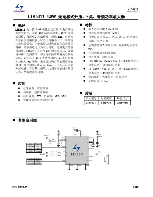
LTK5311 2019.2.20修订LTK5311 4.9W 无电感式升压、F 类、音频功率放大器⏹ 管脚说明及定义PVB A CTR A VBA ASSP CPOU T Top View Bottom View⏹基本电气特性⏹性能特性曲线特性曲线图图1:Input Amplitude VS. OutputPower图2:Input Voltage VS. Output Power图3:Input Voltage VS.Power Crrent图4:Output Power VS.THD+N图5:Frequency VS.THD+N图6:Frequency VS.THD+N1010010001000010100100010000O u t p u t A m p l i t u d e (m V r m s )Input Voltage Amplitude (mVrms )VDD=4.2V AGC_OFF RL=4Ω+33uHVDD=4.2V AGC=MODE4 THD=10% RL=4Ω+33uH VDD=4.2V AGC=MODE1 THD=1% RL=4Ω+33uHInput Amplitude VS Output Amplitude0.010.11100.1110T H D +N %Output Power (W )VDD=4.2V RL=4Ω+33uH Class_D VDD=3.8V RL=4Ω+33uH Class_DOutput Power VS THD+N0.010.111010100100010000T H D +N %Frequency(HZ)VDD=4.2V AGC_OFF PO=1W RL=4Ω+33uHVDD=4.2V AGC_OFF PO=0.5W RL=4Ω+33uHFrequency VS THS+N0.010.111010100100010000T H D +N %Frequency(HZ)VDD=3.8V AGC_OFF PO=1W RL=4Ω+33uHVDD=3.8V AGC_OFF PO=0.5W RL=4Ω+33uHFrequency VS THD+N%图7:Frequency Response图8:Output Power VS.THD+N⏹ 应用说明● Flying 电容Flying 电容C F 用于在电源和Charge Pump 输出CPOUT 之间传递能量,该电容的容值过小会影响负载调整率和输出电流。
G5178Low-Power Off-Line Digital Green-Mode PWM Controller1of 16Global Semiconductor Co.,LTD.1.0General DescriptionThe G5178is a high performance AC/DC power supply controller which uses digital control technology to build peak current mode PWM flyback power supplies.The device together with an external active device (depletion mode NFET or NPN BJT)provides a fast start-up meanwhile achieving ultra-low no-load power consumption.The device directly drives a power BJT and operates in quasi-resonant mode to provide high efficiency along with a number of key built-in protection features while minimizing the external component count,simplifying EMI design and lowering the total bill of material cost.The G5178removes the need for secondary feedback circuitry while achieving excellentline and load regulation.It also eliminates the need for loop compensation components while maintaining stability over all operatingconditions.Pulse-by-pulse waveform analysis allows for a loop response that is much faster than traditionalsolutions,resulting in improved dynamic load response,for both one-time and repetitive load transient.The built-in power limit function enables optimized transformer design inuniversal off-line applications and allows for a wide input voltage range.Global Semiconductor’s innovative proprietary technology ensures that power supplies built with the G5178can achieve both highest average efficiency and zero no-load power consumption,and have fast dynamic load response in a compact form factor.The active start-up scheme enables shortest possible start-up time without sacrificing no-load power loss.DIGITAL PWM ICFeatures◆Very tight constant voltage and constantcurrent regulation over entire operating range ◆Zero power consumption at no-load withlowest system cost (<5mW at 230Vac with typical application circuit)◆Intelligent low power management achieves ultra-low operating current at no-load◆Complies with EPA 2.0energy-efficiencyspecifications with ample margin ◆Intrinsically low common mode noise ◆Adaptive multi-mode PWM/PFM controlimproves efficiency◆Quasi-resonant operation for highest overallefficiency◆Direct drive of low-cost BJT switch ◆Dynamic base current control◆No external compensation componentsrequired◆Primary-side feedback eliminatesopto-isolators and simplifies design◆Optimized 72kHZ PWM switching frequencyachieves best size and efficiency◆EZ-ENI @design enhances manufacturability ◆Built-in soft start◆Built-in short circuit protection and output overvoltage protection◆Built-in current sense resistor short circuit protection◆No audible noise over entire operatingApplications●Compact low power AC/DCadapter/chargers for cellphones,PDAs,digital still cameras ●Linear AC/DC replacementG5178Low-Power Off-Line Digital Green-Mode PWM ControllerRev.1.02of 162.0Products Information2.1Pin configuration2.2Marking Information2.3Series description Pin Name I/O DescriptionV DD P Power supply for control logic.FB I Analog Input Auxiliary voltage sense (used for primary regulation).ASU O Control signal for active start-up device (BJT or depletion NFET).CS I Analog Input Primary current ed for cycle-by-cycle peak current control and limit.GND P Ground.DRVOBase drive for BJT.Part Number Marking InformationG5178GDXXXPart Number DescriptionG5178-00Cable Comp =0mVV DD FB ASUDRV GND CSPin Configuration:G5178Series (Sot23-6)G5178Low-PowerOff-Line Digital Green-Mode PWM Controller 3of 162.4Block diagram3.0Absolute Maximum RatingsParameterSymbol Value Units DC supply voltage range (pin 1,I DD =20mA max)V DD -0.3to 18.0V Continuous DC supply current at V DD pin (V DD =15V)I DD20mA ASU output (Pin 3)-0.3to 18.0V DRV output (Pin 6)-0.3to 4.0V FB input (Pin 2,I FB ≤10mA)-0.7to 4.0V CS input (Pin 4)-0.3to 4.0V Maximum junction temperature 150℃Storage temperature–65to 150℃Lead temperature during IR reflow for ≤15seconds T J MAX 260℃Thermal resistance junction-to-ambient T STG 190℃/W ESD ratingT LEAD 2,000V Latch-up test per JEDEC 78θJA ±100mAG5178Low-Power Off-Line DigitalGreen-Mode PWM ControllerRev.1.04of16 4.0Typical ApplicationThe G5178contains a controller for a yback circuit.Figure4.1G5178Typical Application Circuit5.0Electrical Characteristics(V DD=12V,-40C≤T A≤+85C,unless otherwise specified)Symbol Parameter Test Conditions Min Typ Max Unit Supply Voltage(Pin1)V DD(MAX)Maximum operatingvoltage(Note1)16V V DD(ST)Start-up threshold V DD rising10.011.012.0VV DD(UVL)Under voltage lockoutthresholdV DD falling 3.8 4.0 4.2VI IN(ST)Start-up current V DD=10V 1.0 1.7 3.0uAI DDQ Quiescent current No I B current 2.7 4.0mAV ZB Zener breakdown voltage Zener current=5mA18.519.520.5V Feedback(Pin2)I BVS Input leakage current V SENSE=2V1uAV FB Nominal voltage threshold TA=25°C,negative edge 1.518 1.533 1.548VG5178Low-PowerOff-Line Digital Green-Mode PWM Controller 5of 16SymbolParameter Test ConditionsMin TypMax UnitV FB (MAX)Output OVP threshold -00(Note 1)TA=25°C,negative edge 1.834V V FB (MAX)Output OVP threshold -01(Note 1)TA=25°C,negative edge Load=100%1.926VASU Section (Pin3)V ASUMaximum operatingvoltage(Note1)16V R VDD_ASUResistance between V DDand ASU830kΩCS Section (Pin4)V OCP Over current threshold 1.11 1.15 1.19V V IPK(HIGH)I CS regulation upper limit (Note 1)1.0V V IPK(LOW)I CS regulation lower limit (Note 1)0.23VI LKInput leakage current V CS =1.0V 1uADRV Section (Pin6)R DS(ON)LODRV low level ON-resistanceI SINK =5mA 13ΩF SWSwitching frequency (Note 2)>50%load72kHzNotes:Note 1.These parameters are not 100%tested,guaranteed by design and characterization.Note 2.Operating frequency varies based on the load conditions,see Section 9.6for more details.G5178Low-PowerOff-LineDigital Green-ModePWM ControllerRev.1.06of16 6.0Typical Performance CharacteristicsNotes:Note1.Operating frequency varies based on the load conditions,see Section8.6formore details.G5178Low-PowerOff-Line Digital Green-Mode PWM Controller 7of 167.0Theory of OperationTheG5178is a digital controller which uses a new,proprietary primary-side control technology to eliminate the opto-isolated feedback and secondary regulation circuits required in traditional designs.This results in a low-cost solution for low power AC/DC adapters.The core PWM processor uses fixed-frequency Discontinuous Conduction Mode (DCM)operation at higher power levels and switches to variable frequency operation at light loads to maximize efficiency.Furthermore,G5178’s digital control technology enables fast dynamic response,tight output regulation,and full featured circuit protection with primary-side control.Referring to the block diagram in Figure 7.1,the digital logic control block generates the switching on-time and off-time information based on the output voltage and current feedback signal and provides commands to dynamically control theexternal BJT base current.The system loop is automatically compensated internally by a digital error amplifier.Adequate system phase margin and gain margin are guaranteed by design and no external analog components are required forloop compensation.The G5178uses an advanced digital control algorithm to reduce system design time and increase reliability.Furthermore,accurate secondary constant-current operation is achieved without the need for any secondary-side sense and control circuits.The G5178uses adaptive multi-mode PWM/PFM control to dynamically change the BJT switching frequency for efficiency,EMI,and power consumption optimization.In addition,it achieves unique BJT quasi-resonant switching to further improve efficiency and reduce EMI.Built-in single-point fault protection features include overvoltage protection (OVP),output short circuit protection (SCP),over current protection (OCP),and ISENSE fault detection.In particular,it ensures that power supplies built with the G5178can meet 5-star energy saving requirement and achieve fast dynamic load response.G5178’s digital control scheme is specifically designed to address the challenges and trade-offs of power conversion design.This innovative technology is ideal for balancing new regulatory requirements for green mode operation with more practical design considerations such as lowest possible cost,smallest size and high performance output control.G5178Low-Power Off-Line Digital Green-Mode PWM Controller7.1Pin DetailPin1–V DDPower supply for the controller during normal operation.The controller will start upwhen V DD reaches11.0V(typical)and will shut-down when the V DD voltage is4.0V(typical).A decoupling capacitor of0.1μF or so should be connected between theV DD pin and GND.Pin2–FBSense signal input from auxiliary winding.This provides the secondary voltagefeedback used for output regulation.Pin3–ASUControl signal for active startup device.This signal is pulled low after start-up isfinished to cut off the active device.Pin4–CSPrimary current ed for cycle-by-cycle peak current control and limit.Pin5–GNDGround.Pin6–DRVBase drive for the external power BJT switch.7.2Active Start-up and Soft-startRefer to Figure 4.1for active start-up circuits using external depletion NFET and BJTrespectively.Prior to start-up,the depletion NFET or the BJT is turned on,allowing the start-upcurrent to charge the V DD bypass capacitor.When the VCC bypass capacitor is charged to avoltage higher than the start-up threshold V DD(ST),the ENABLE signal becomes active and theG5178commences soft start function.During this start-up process an adaptive soft-start controlalgorithm is applied,where the initial output pulses will be small and gradually get larger untilthe full pulse width is achieved.The peak current is limited cycle by cycle by the IPEAKcomparator.If at any time the V DD voltage drops below undervoltage lockout(UVLO)thresholdV DD(UVL)then the G1578goes to shutdown.At this time ENABLE signal becomes low and theCC capacitor begins to charge up again towards the start-up threshold to initiate a new soft-startprocess.While the ENABLE signal initiates the soft-start process,it also pulls down the ASU pinvoltage at the same time,which turns off the depletion NFET or the BJT,thus minimizing theno-load standby power consumption.Rev.1.08of16G5178Low-PowerOff-LineDigital Green-Mode PWM Controller 9of 16Figure 7.1:Start-up Sequencing Diagram7.3Understanding Primary FeedbackFigure 7.2illustrates a simplified flyback converter.When the switch Q1conducts during t ON (t),the current ig(t)is directly drawn from rectified sinusoid vg(t).The energy Eg(t)is stored in the magnetizing inductance L M .The rectifying diode D1is reverse biased and the load current IO is supplied by the secondary capacitor CO.When Q1turns off,D1conducts and the stored energy Eg(t)is delivered to the output..Figure 7.2:Simplified Flyback ConverterG5178Low-Power Off-Line Digital Green-Mode PWM ControllerRev.1.010of 16In order to tightly regulate the output voltage,the information about the output voltage and load current need to be accurately sensed.In the DCM fl yback converter,this information can be read via the auxiliary winding or the primary magnetizing inductance (L M ).During the Q1on-time,the load current is supplied from the output filter capacitor CO.The voltage across L M is vg(t),assuming the voltage dropped across Q1is zero.The current in Q1ramps up linearly at a rate of:di g (t)/dt=v g (t)/L M(7.1)At the end of on-time,the current has ramped up to:i g _peak (t)=v g (t)*t ON /L M (7.2)This current represents a stored energy of:E g =L M /2*I g _b (peak)2(7.3)When Q1turns off at to,ig(t)in L M forces a reversal of polarities on all windings.Ignoring the communication-time caused by the leakage inductance L K at the instant of turn-off to,the primary current transfers to the secondary at a peak amplitude of:i d t)=N P /N S *I g_peak (t)(7.4)Assuming the secondary winding is master,and the auxiliarywinding is slave,Figure 7.3:Auxiliary Voltage WaveformsThe auxiliary voltage is given by:V AUX =N AUX /N S (V0+△V)(7.5)and reflects the output voltage as shown in Figure 7.3.The voltage at the load differs from the secondary voltage by a diode drop and IR losses.Thus,if the secondary voltage is always read at a constant secondary current,the difference between the output voltage and the secondary voltage will be a fixed ΔV.Furthermore,if the voltage can be read when the secondary currentis small,ΔV will also be small.With the G5178,ΔV can be ignored..The real-time waveform analyzer in the G5178reads this information cycle by cycle.The part then generates a feedback voltage VFB.The VFB signal precisely represents the output voltage under most conditions and is used to regulate the output voltage.7.4Constant Voltage OperationAfter soft-start has been completed,the digital control block measures the output conditions.It determines output power levels and adjusts the control system according to a light load or heavy load.If this is in the normal range,the device operates in the Constant Voltage(CV) mode,and changes the pulse width(T ON)and off time(T OFF)in order to meet the output voltage regulation requirements.If no voltage is detected on FB it is assumed that the auxiliary winding of the transformer is either open or shorted and the G5178shuts down.7.5Constant Current OperationThe constant current(CC)mode is useful in battery charging applications.During this mode of operation the G5178will regulate the output current at a constant level regardless of the output voltage,while avoiding continuous conduction mode.To achieve this regulation the G5178senses the load current indirectly through the primary current.The primary currentis detected bythe CS pin through a resistor from the BJT emitter to ground.Figure7.4:Power Envelope11of167.6Multi-Mode PWM/PFM Control and Quasi-Resonant SwitchingThe G5178uses a proprietary adaptive multi-mode PWM/PFM control to dramatically improvethe light-load efficiency and thus the overall average effi ciency.During the constant voltage(CV)operation,the G5178normally operates in apulse-width-modulation(PWM)mode during heavy load conditions.In the PWM mode,theswitching frequency keeps around constant.As the output load I OUT is reduced,the on-time t ON isdecreased,and the controller adaptively transitions to a pulse-frequency-modulation(PFM)mode.During the PFM mode,the BJT is turned on for a set duration under a given instantaneousrectified AC input voltage,but its off time is modulated by the load current.With a decreasingload current,the off time increases and thus the switching frequency decreases.When the switching frequency approaches to human ear audio band,the G5178transitions to asecond level of PWM mode,namely Deep PWM mode(DPWM).During the DPWM mode,the switching frequency keeps around25kHz in order to avoid audible noise.As the load currentis further reduced,the G5178transitions to a second level of PFM mode,namely Deep PFMmode(DPFM),which can reduce the switching frequency to a very low level.Although theswitching frequency drops across the audible frequency range during the DPFM mode,theoutput current in the power converter has reduced to an insignifi cant level in the DPWM modebefore transitioning to the DPFM mode.Therefore,the power converter practically produces noaudible noise,while achieving high efficiency across varying load conditions.As the load currentreduces to very low or no-load condition,the G5178transitions from the DPFM to the third levelof PWM mode,namely Deep-Deep PWM mode(DDPWM),where the switching frequency isfixed at around2.1kHz.The G5178also incorporates a unique proprietary quasiresonant switching scheme that achievesvalley-mode turn on for every PWM/PFM switching cycle,during all PFM and PWM modes andin both CV and CC operations.This unique feature greatly reduces the switching loss and dv/dtacross the entire operating range of the power supply.Due to the nature of quasi-resonantswitching,the actual switching frequency can vary slightly cycle by cycle,providing theadditional benefit of reducing EMI.Together these innovative digital control architecture andalgorithms enable the G5178to achieve highest overall efficiency and lowest EMI,withoutcausing audible noise over entire operating range.Rev.1.012of167.7Zero Power No-Load OperationAt the no-load condition,the G5178is operating in the DPFM mode,where the switchingfrequency can drop as low as275Hz and still maintain tight closed-loop control of outputvoltage.The distinctive DPFM operation allows the use of a relatively large pre-load resistorwhich helps reduce the no-load power consumption.In the meanwhile,the G5178implements anintelligent low-power management technique that achieves ultra-low chip operating current atthe noload,typically less than400μA.One important feature of the G5178is that it directlydrives a low-cost BJT switch.Unlike a power MOSFET,the BJT is a current-driven device thatdoes not require a high driving voltage.As a result,the UVLO threshold of the iW1700isdesigned to be as low as4.0V(typical).The power supply system design can fully utilize thislow UVLO feature to have a low VCC voltage at the no-load operation in order to minimize theno-load power.In addition,the active start-up scheme with depletion NFET eliminates thestartup resistor power consumption after the ENABLE signal becomes active.All together thesefeatures ensure with the lowest system cost power supplies built with the G5178can achieve lessthan5mW no-load power consumption at230Vac input and maintain very tight constant voltageand constant current regulation over the entire operating range including the no-load operation.While achieving ultra-low no-load power consumption,the G5178implements innovativeproprietary digital control technology to intelligently detect load transient events,and ensureadaptive fast response.7.8Variable Frequency Operation ModeAt each of the switching cycles,the falling edge of FB will be checked.If the falling edge of FBis not detected,the off-time will be extended until the falling edge of FB is detected.Themaximum allowed transformer reset time is110μs.When the transformer reset time reaches110μs,the G5178shuts off.7.9Internal Loop CompensationThe G5178incorporates an internal Digital Error Amplifier with no requirement for externalloop compensation.For a typical power supply design,the loop stability is guaranteed to provideat least45degrees of phase margin and-20dB of gain margin.13of167.10Voltage Protection FeaturesThe secondary maximum output DC voltage is limited by the G5178When the FB signalExceeds the output OVP threshold at point1indicated in Figure7.3the G5178huts down.The G5178protects against input line undervoltage by setting a maximum T ON time.Sinceoutput power is power is proportional to the squared V IN T ON product,then for a given outputpower,as V IN decreases the T ON will increase.Thus by knowing when the maximum T ON timeoccurs the G5178detects that the minimum V IN is reached,and shuts down.The maximum t ONlimit is set to13.8us.Also,the G5178monitors the voltage on the V DD pin and when the voltageon this pin is below UVLO threshold the IC shuts down immediately.When any of these faults are met the IC remains biased to discharge the V DD supply.Once V DDdrops below UVLO threshold,the controller resets itself and the initiates a new soft-start cycle.The controller continues attempting start-up until the fault condition is removed.7.11PCL,OCP and SRS ProtectionPeak-current limit(PCL),over-current protection(OCP)and sense-resistor short protection(SRSP) are features built-in to the G5177.With the FB pin the G5178monitor the peak primary current.This allows for cycle by cycle peak current control and limit.When the primary peak currentmultiplied by the FB resistor is greater than1.15V,over current(OCP)is detected and the ICwill immediately turn off the base driver until the next cycle.The output driver will send out aswitching pulse in the next cycle,and the switching pulse will continue if the OCP threshold isnot reached;or,the switching pulse will turn off again if the OCP threshold is reached.If theOCP occurs for several consecutive switching cycles,the G5178down.If the FB resistor is shorted there is a potential danger of the over current condition not beingdetected.Thus,the IC is designed to detect this sense-resistor-short fault after startup and shutdown immediately.The VDD ll be discharged since the IC remains biased.Once VDD ps belowthe UVLO threshold,the controller resets itself and then initiates a new soft-start cycle.Thecontroller continues attempting to startup,but does not fully startup until the fault condition isremoved.Rev.1.014of167.12Dynamic Base Current ControlOne important feature of the G5178is that it directly drives a BJT switching device with dynamic base current control to optimize performance.The BJT base current ranges from13mA to40mA,and is dynamically controlled according to the power supply load change.The higherthe output power,the higher the base current.Specifically,the base current is related to V IPK,asshown in Figure8.5.Figure7.5:Base Drive Current vs.V IPK7.13Cable Drop CompensationThe G5178incorporates an innovative method to compensate for any IR drop in the secondarycircuitry including cable and cable connector.A2.5W adapter with5V DC output has3%deviation at0.5A load current due to the drop across a24AWG,1.8meter DC cable withoutcable compensation.The G5178compensates for this voltage drop by providing a voltage offsetto the feedback signal based on the amount of load current detected.15of16Rev.1.016of 168.0Package InformationSot23-6SymbolDimension in Millimeters Dimensions in Inches Min Max Min Max A2.6923.0990.1060.122B1.397 1.8030.0550.071C-- 1.450--0.057D0.3000.5000.0120.020F0.950.037H0.0800.2540.0030.010I0.0500.1500.0020.006J2.6003.0000.1020.118M0.3000.6000.0120.024θ0°10°0°10°Data and specifications subject to change without notice.This product has been designed and qualified for Industrial Level and Lead-Free.Qualification Standards can be found on GS's Web site.Global Semiconductor HEADQUARTERS:Scotia Centre ,4th Floor ,P.O.Box 2804,George Town ,Grand Cayman KY1-1112,CaymanVisit us at for sales contact information.。
LM2576中文资料———————————————————————————目录概述 (3)1.LM2576简介 (3)1.1 性能 (3)1.2 外形图 (6)1.3 订购信息 (6)1.4 管脚定义 (7)2.LM2576应用举例 (7)2.1 基本应用设计 (7)2.1.1 应用分析 (7)2.1.2 外围元件的选择 (9)2.1.3应用注意事项 (10)2.2 工作模式可控应用设计 (10)2.3 1.2V至55V的可调3A低输出纹波电源 (10)页脚内容12.4 输入欠压锁定电源 (11)3.LM2576测试电路和PCB布局原则 (11)页脚内容2概述LM2576系列开关稳压集成电路是线性三端稳压器件(如78xx系列端稳压集成电路)的替代品,它具有可靠的工作性能、较高的工作效率和较强的输出电流驱动能力,从而为MCU的稳定、可靠工作提供了强有力的保证。
1.LM2576简介1.1 性能LM2576系列是美国国家半导体公司生产的3A电流输出降压开关型集成稳压电路,它内含固定频率振荡器(52kHz)和基准稳压器(1.23V),并具有完善的保护电路,包括电流限制及热关断电路等,利用该器件只需极少的外围器件便可构成高效稳压电路。
LM2576系列包括LM2576(最高输入电压40V)及LM2576HV(最高输入电压60V)二个系列。
各系列产品均提供有3.3V(-3.3)、5V(-5.0)、12V(-12)、15V(-15)及可调(-ADJ)等多个电压档次产品。
此外,该芯片还提供了工作状态的外部控制引脚。
图1LM2576系列开关稳压集成电路的主要特性如下[2]:●最大输出电流:3A;页脚内容3●最高输入电压:LM2576为40V,LM2576HV为60V;●输出电压:3.3V、5V、12V、15V和ADJ(可调)等可选;●振东频率:52kHz;●转换效率:75%~88%(不同电压输出时的效率不同);●控制方式:PWM;●工作温度范围:-40℃~+125℃●工作模式:低功耗/正常两种模式可外部控制;●工作模式控制:TTL电平兼容;●所需外部元件:仅四个(不可调)或六个(可调);●器件保护:热关断及电流限制;●封装形式:TO-220或TO-263。
TI推出业界领先的多相双向电流控制器
高度集成的降压-升压控制器可在双车载电池系统之间实现有效的电力传输
2017年3月21日,北京讯德州仪器(TI)近日推出业界领先的全集成型多相双向DC/DC电流控制器,该器件可在48V和12V的双车载电池系统之间有效传输每相大于500W的电力。
高度集成的LM5170-Q1模拟控制器采用创新的平均电流模式控制方法,克服了当今元件数量多、全数字控制方案的挑战。
如需了解更多信息并获得样片和评估模块,敬请访问TI/lm5170q1-pr-cn。
TI将出席于2017年3月27日至29日在佛罗里达州坦帕举行的应用能源电子展(APEC),并在701号展位展出这款LM5170-Q1控制器。
LM5170-Q1是TI业界领先的DC/DC转换器、控制器和电荷泵产品组合中的最新产品,帮助工程师实现创新并打造差异化的电源设计。
混合动力汽车使用高压48 V电池和标准的12 V汽车电池。
设计工程师通常采用数字控制方案管理这些双电池系统,包括多个分立元件,如电流检测放大器、栅极驱动器和保护电路。
这些全数字控制方案不仅体积庞大,而且价格昂贵。
为了解决这一挑战,同时提高性能和系统可靠性,TI提供了一种。
lm2577升压工作原理LM2577是一种常用的升压型DC-DC转换器芯片,其工作原理基于开关电源技术。
本文将详细介绍LM2577升压工作原理。
一、LM2577的基本结构和工作原理LM2577芯片由输入电压检测电路、PWM控制电路、开关管驱动电路、功率开关管、输出电压反馈电路和输出电流保护电路等组成。
1. 输入电压检测电路:LM2577的输入电压检测电路主要用于检测输入电压是否达到芯片工作的最低电压要求。
如果输入电压低于最低电压要求,芯片将不会启动。
2. PWM控制电路:PWM控制电路是LM2577的核心部分,用于产生高频脉冲信号。
这个信号的占空比决定了开关管的导通时间和关断时间,从而影响转换效率和输出电压。
3. 开关管驱动电路:开关管驱动电路用于驱动功率开关管。
当PWM控制电路产生高电平信号时,开关管导通,当PWM控制电路产生低电平信号时,开关管关断。
4. 功率开关管:功率开关管是LM2577的核心元件,它可以实现输入电压的升压。
当开关管导通时,输入电压通过电感储能,当开关管关断时,储能电感将其储存的能量传递给输出回路,实现输出电压的升压。
5. 输出电压反馈电路:输出电压反馈电路用于监测输出电压,并将反馈信号送回PWM控制电路,通过调节占空比来稳定输出电压。
6. 输出电流保护电路:输出电流保护电路用于监测输出电流,当输出电流超过一定阈值时,保护电路将关闭开关管,以保护电路和负载。
二、LM2577的升压工作原理LM2577的升压工作原理可以分为四个阶段:导通、储能、关断和输出。
1. 导通阶段:在导通阶段,PWM控制电路产生高电平信号,驱动开关管导通。
此时,输入电压通过电感储能,并将能量传递给输出回路,输出电压开始升高。
2. 储能阶段:在储能阶段,开关管关断,电感储能器将能量储存起来。
此时,输出电压继续上升。
3. 关断阶段:在关断阶段,PWM控制电路产生低电平信号,驱动开关管关断。
此时,储能电感将其储存的能量传递给输出回路,输出电压继续上升。
1MHz单周期控制同步整流Buck变换器的设计
任琦梅;姜建
【期刊名称】《电测与仪表》
【年(卷),期】2014(000)009
【摘要】提高功率变换器功率密度的有效方法是加大开关频率。
传统的单周期控
制芯片 IR1150只能工作到200 kHz的开关频率,为此提出了一种1 MHz工作频
率的单周期控制同步整流Buck变换器实现方案,控制电路采用
“UC3825+TPS28225”这两款芯片实现,其中UC3825作为主控芯片,TPS28225作为驱动芯片。
分析了整个系统工作原理,并对同步整流Buck变换器的主开关管、同步整流管、输出滤波器和积分器等进行了详细分析及设计。
制作了一台1.8V、
5A输出的样机,样机运行稳定,额定效率可达80.74%。
实验结果验证了该设计方案的有效性。
【总页数】4页(P102-105)
【作者】任琦梅;姜建
【作者单位】河南城建学院,河南平顶山467036;河南城建学院,河南平顶山467036
【正文语种】中文
【中图分类】TM46
【相关文献】
1.基于LTC3879高效同步整流BUCK变换器的设计 [J], 杨帆
2.同步整流buck变换器低功耗驱动电路设计 [J], 高庆;孙金中;郭锐
3.低压大电流同步整流Buck变换器的设计 [J], 邵静宜
4.低压大电流同步整流Buck变换器的设计 [J], 邵静宜;
5.移相双重同步整流Buck变换器的研究与设计 [J], 张德超; 秦建鑫; 杨艳
因版权原因,仅展示原文概要,查看原文内容请购买。
HX711电路优点及特性:HX711是一款专为高精度秤重传感器而设计的24位A/D转换器芯片。
与同类型其它芯片相比,该芯片集成了包括稳压电源、片内时钟振荡器等其它同类型芯片所需要的外围电路,具有集成度高、响应速度快、抗干扰性强等优点、降低了电子秤的整机成本,提高了整机的性能和可靠性。
该芯片与后端MCU芯片的接口和编程非常简单,所有控制信号由管脚驱动,无需对芯片内部的寄存器编程。
输入选择开关可任意选取通道A或通道B,与其内部的低噪声可编程放大器相连。
通道A的可编程增益为128或64,对应的满额度差分输入信号幅值分别为±20mV或±40mV。
通道B则为固定的64增益,用于系统参数检测。
芯片内提供的稳压电源可以直接向外部传感器和芯片内的A/D转换器提供电源,系统板上无需另外的模拟电源。
芯片内的时钟振荡器不需要任何外接部件。
上电自动复位功能简化了开机的初始化过程。
引脚功能及电器特性表引脚功能表3 输入通道和增益选择管脚说明模拟输入通道A模拟差分输入可直接与桥式传感器的差分输出相接。
由于桥式传感器输出的信号较小,为了充分利用A/D转换器的输入动态范围,该通道的可编程增益较大,为128或64。
这些增益所对应的满量程差分输入电压分别±20mV或±40mV。
通道B为固定的增益,所对应的满量程差分输入电压为±40mV。
通道B 应用于包括电池在内的系统参数检测。
供电电源数字电源(DVDD)应使用与MCU芯片相同的数字供电电源。
HX711芯片内稳压电路可同时向A/D转换器和外部传感器提供模拟电源。
稳压电源的供电电压(VSUP)可与数字电源(DVDD)相同。
稳压电源的输出电压值(VAVDD)由外部分电阻R1、R2和芯片的输出参考电压VBG决定(图4),VAVDD=VBG(R1+ R2)/ R2。
应选择该输出电压比稳压电源的输入电压(VSUP)低至少100mV。
如果不使用芯片内的稳压电路,管脚VSUP和管脚AVDD应相连,并接到电压为2.6-5.5V 的低噪声模拟电源。