双通道恒流LED控制芯片RM9002E中文规格书(精)
- 格式:doc
- 大小:88.50 KB
- 文档页数:10
单通道恒流LED可控硅调光芯片RM9005E规格书产品概述:RM9005E是单通道调光LED 恒流驱动控制芯片,可直接驱动高压LED灯串,输出电流由外接SENSE电阻设置,输出电流范围在5mA~80mA,且输出电流恒定在设定值。
芯片系统结构简单,外围元器件极少,线路简单。
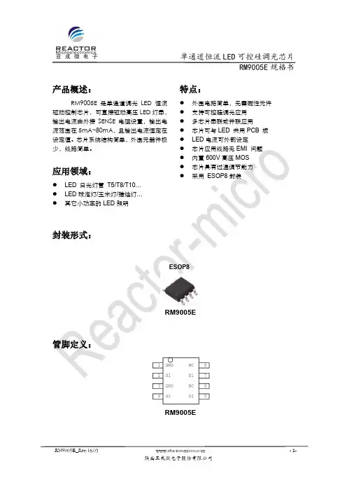
应用领域:●LED 日光灯管T5/T8/T10…●LED球泡灯/玉米灯/蜡烛灯…●其它小功率的LED照明特点:●外围电路简单,无需磁性元件●支持可控硅调光应用●多芯片串联或并联应用●芯片可与LED 共用PCB 板●LED电流可外部设定●芯片应用线路无EMI 问题●内置600V高压MOS●芯片具有过温调节能力●采用ESOP8封装封装形式:ESOP8RM9005E 管脚定义:RM9005E单通道恒流LED可控硅调光芯片RM9005E规格书管脚说明:管脚名称管脚描述D1,D2 芯片正极GND 芯片负极(接地端)S1,S2 芯片电流采样端NC 无定义管脚极限参数:符号参数参数范围S1 电流采样输入电压-0.3v to 7vTJ 工作结温范围-40℃to 150℃Tc 工作温度-40℃to 100℃TSTG 储存温度范围-55℃to 150℃注:极限值是指超出该工作范围,芯片有可能损坏。
推荐工作范围是指在该范围内,器件功能正常,但并不完全保证满足个别性能指标。
电气参数定义了器件在工作范围内并且在保证特定性能指标的测试条件下的直流和交流电参数规范。
对于未给定上下限值的参数,该规范不予保证其精度,但其典型值合理反映了器件性能。
典型应用:图1:典型驱动方案单通道恒流LED可控硅调光芯片RM9005E规格书电气参数:(无特别说明情况下,TA =25 ℃)符号参数条件最小值典型值最大值单位V on1工作电压最小值S1=30mA 6 - - V V on2工作电压最小值S1=30mA 7 - - V V DS1驱动端峰值电压600 - - V V DS2驱动端峰值电压600 - - VI S1工作电流环境温度100℃ 5 - 80 mAI S2工作电流环境温度100℃ 6 - 80 mA Vref1 恒流电压基准25℃- 0.6- V Vref2 恒流电压基准25℃- 0.6- V Idd1 静态工作电流Vd=10V - 0.3 - mA Idd2 静态工作电流Vd=10V - 0.3 - mA OTP 过温调节点- 130 - ℃功能框图:单通道恒流LED可控硅调光芯片RM9005E规格书工作原理:针对于线性电路,D1和S1限定输入端口的输入电流,使输入有电压存在情况下就有一定的电流提供给可控硅调光器,保证可控硅调光器的正常工作,避免调光过程中的闪烁现象,D2和S2控制LED的正常工作,由于输入电压变化(或除LED串之外的剩余电压)引起IC两端所承载电压的波动,使IC自身功耗发生改变,所以在整个电路中D1和S2起到承担剩余功率、恒定LED串电流、控制LED灯具温度的特性。
3M SPEEDGLAS 9002D 产品说明书焊接前为保护您的安全请在使用SEEDGLAS 9002D之前仔细阅读本说明书。
根据本手册图A:1的说明来安装本产品。
根据个人的需要调节头罩,头带的直径和高度都要进行调节,面罩和面部的角度应该根据图A:2所示进行调节。
所有SPEEDLAS自动变光焊接滤光片可用于电弧焊和气体切割。
电弧焊接包括熔化极气体保护焊(MIG,MAG)、不熔化极气体保护焊(TIG)、手工电焊条电弧焊(SMAW)、等离子弧焊接和吹气碳电弧焊接。
当滤光片处于关机状态时可用于气割或气焊,关机状态遮光号为5-6。
暗态的遮光号标在产品上。
请根据欧洲标准EN379(或者欧洲标准:EN169)选择适合的遮光号。
SPEEDGLAS自动变光焊接滤光片按照产品上所标注的最大遮光号来防护有害的紫外和红外光线。
对紫外和红外光线的防护是永久的,不论是在亮态还是在暗态。
在电池和电子系统故障时,焊工仍然得到紫外和红外光线的防护,这时的遮光号是产品上标注的最大遮光号。
焊接滤光片有两个独立的感光探头,只要有弧光照射,镜片就要变暗。
电源是两个3伏锂电池。
焊接镜片在最后一次弧光照射后约60分钟会自动关机。
注意:SPEEDGLAS 9002D自动变光焊接滤光片必须与原装SPEEDGLAS 9000 焊接面罩、内部保护镜片和外部保护镜片一起使用。
注意:SPEEDGLAS 9002D焊接面罩不适合用于‘仰焊’、激光焊和激光切割。
标识:每一个产品都标有正确的遮光号或者遮光号的范围,在焊接前必须确认选择了正确的遮光号。
眼睛和面部防护的分类分别依据EN379(或EN175)。
产品上标注的其它标识是根据相关欧洲标准制定。
下面是一个举例:注意:上面只是一个例子,有效的分类标注在产品上。
在焊帽和外部保护片上,标有防高速颗粒物冲击分类标识,F代表低速冲击防护(45m/s),B代表中速冲击防护(12m/s),如果产品符合极端温度(-5℃-+55℃)的要求,则会标有T。
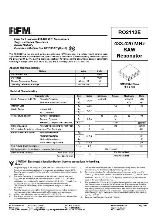
RF Monolithics, Inc.Phone: (972) 233-2903Fax: (972) 387-8148E-mail: info@ Page 1 of 2RFM Europe Phone: 44 1963 251383Fax: 44 1963 251510 ©1999 by RF Monolithics, Inc. The stylized RFM logo are registered trademarks of RF Monolithics, Inc.RO2112E-042505CAUTION: Electrostatic Sensitive Device. Observe precautions for handling.Notes:Electrical CharacteristicsCharacteristicSymNotes Minimum TypicalMaximum Units Center Frequency (+25 °C)Absolute Frequencyf C 2,3,4,5433.345433.495MHz Tolerance from 433.420 MHz∆f C ±75kHz Insertion Loss IL 2,5,6 1.21.8dBQuality Factor Unloaded Q Q U 5,6,750 Ω Loaded Q Q L Temperature StabilityTurnover Temperature T O 6,7,8102535°CTurnover Frequencyf O f C Frequency Temperature CoefficientFTC 0.032ppm/°C 2Frequency AgingAbsolute Value during the First Year |f A |1≤10ppm/yr DC Insulation Resistance between Any Two Terminals51.0M ΩRF Equivalent RLC ModelMotional Resistance R M 5, 7, 9ΩMotional Inductance L M µH Motional Capacitance C M fF Shunt Static CapacitanceC O 5, 6, 9pF Test Fixture Shunt InductanceL TEST2, 7nHLid Symbolization (in addition to Lot and/or Date Codes)526 // YWWSStandard Reel Quantity Reel Size 7 Inch 10500 Pieces/Reel Reel Size 13 Inch3000 Pieces/Reel•Ideal for European 433.420MHz Transmitters •Very Low Series Resistance •Quartz Stability•Complies with Directive 2002/95/EC (RoHS)The RO2112E is a true one-port, surface-acoustic-wave (SAW) resonator in a surface-mount, ceramic case.It provides reliable, fundamental-mode, quartz frequency stabilization of fixed-frequency transmitters operat-ing at 433.420MHz. This SAW is designed specifically for remote-control and wireless security transmitters operating in Europe under ETSI I-ETS 300 220 and in Germany under FTZ 17 TR 2100.Absolute Maximum RatingsRatingValue Units Input Power Level 0dBm DC voltage12VDC Storage Temperature Range -40 to +125°C Operating Temperature Range-40 to +105°C433.420 MHzSAW ResonatorRO2112E1.Frequency aging is the change in f C with time and is specified at +65°C or less. Aging may exceed the specification for prolonged temperatures above +65°C. Typically, aging is greatest the first year after manufacture, decreasing in subse-quent years.2.The center frequency, f C , is measured at the minimum insertion loss point, IL MIN , with the resonator in the 50Ω test system (VSWR ≤ 1.2:1). The shunt inductance, L TEST , is tuned for parallel resonance with C O at f C . Typically, f OS-CILLATOR or f TRANSMITTER is approximately equal to the resonator f C .3.One or more of the following United States patents apply: 4,454,488 and 4,616,197.4.Typically, equipment utilizing this device requires emissions testing and govern-ment approval, which is the responsibility of the equipment manufacturer.5.Unless noted otherwise, case temperature T C =+25°C±2°C.6.The design, manufacturing process, and specifications of this device are subject to change without notice.7.Derived mathematically from one or more of the following directly measured parameters: f C , IL, 3dB bandwidth, f C versus T C , and C O .8.Turnover temperature, T O , is the temperature of maximum (or turnover) fre-quency, f O . The nominal frequency at any case temperature, T C , may be calcu-lated from: f =f O [1-FTC (T O -T C )2]. Typically oscillator T O is approximately equal to the specified resonator T O .9.This equivalent RLC model approximates resonator performance near the reso-nant frequency and is provided for reference only. The capacitance C O is the static (nonmotional) capacitance between the two terminals measured at low frequency (10MHz) with a capacitance meter. The measurement includes para-sitic capacitance with "NC” pads unconnected. Case parasitic capacitance is approximately 0.05pF. Transducer parallel capacitance can by calculated as: C P ≈C O -0.05pF.10.Tape and Reel Standard Per ANSI / EIA 481.Pb433.420 MHz SAW ResonatorRF Monolithics, Inc.Phone: (972) 233-2903Fax: (972) 387-8148E-mail: info@ Page 2 of 2RFM Europe Phone: 44 1963 251383Fax: 44 1963 251510 ©1999 by RF Monolithics, Inc. The stylized RFM logo are registered trademarks of RF Monolithics, Inc.RO2112E-042505Equivalent LC Mode lTemperature CharacteristicsThe curve shown on the right accounts for resonator contribution only and does not include LC component temperature contributions .Pin Connection1NC 2Terminal 3NC 4NC 5Terminal 6NCPower TestElectrical ConnectionsThe SAW resonator is bidirectional and may be installed with either orientation.The two terminals are interchangeable and unnumbered. The callout NC indi-cates no internal connection. The NC pads assist with mechanical positioning and stability. External grounding of the NC pads is recommended to help reduce parasitic capacitance in the circuit.Typical Test CircuitThe test circuit inductor, L TEST , is tuned to resonate with the static capacitance, C O , at F C .Electrical TestTypical Application CircuitsCase DimensionsDimensionmm Inches Min Nom Max Min Nom Max A 2.87 3.0 3.130.1130.1180.123B 2.87 3.0 3.130.1130.1180.123C 1.12 1.25 1.380.0440.0490.054D 0.770.90 1.030.0300.0350.040E 2.67 2.80 2.930.1050.1100.115F 1.47 1.6 1.730.0580.0630.068G 0.720.850.980.0280.0330.038H 1.37 1.5 1.630.0540.0590.064I 0.470.600.730.0190.0240.029J1.171.301.430.0460.0510.056。

Optoway TRS-9002CG*********************************************************************************************************************************************************************************************************************************************************************************************************************************************OPTOWAY TECHNOLOGY INC. No .38, Kuang Fu S. Road, Hu Kou, Hsin Chu Industrial Park, Hsin Chu, Taiwan 3031TRS-9002CG / TRS-9002CTG / TRS-9002CFG5V / 1310 nm / 2.5 Gbps RoHS Compliant Optical Single-Mode Transceiver*********************************************************************************************************************************************************************FEATURESl Duplex SC Single Mode Transceiver: TRS-9002CG l Duplex ST Single Mode Transceiver: TRS-9002CTG l Duplex FC Single Mode Transceiver: TRS-9002CFG l SONET OC-48 SR / SDH STM-16 (I-16) Compliant l Fiber Channel 2X/1X SM-LC-L FC-PI Compliant l IEEE 802.3z Gigabit Ethernet 1000BASE-LX Compliantl Industry Standard 1 x 9 Footprint l 0 to 70o C Operating : TRS-9002CG l -40 to 85o C Operating : TRS-9002CAG l Single +5 V Power Supply l RoHS Compliantl TTL Signal Detect Outputl Wave Solderable and Aqueous Washablel Class 1 Laser International Safety Standard IEC 60825 CompliantAPPLICATIONSl Switch to Switch Interfacel High Speed Interface for File Servers l High Performance DesktopsDESCRIPTIONThe TRS-9002CG series single mode transceivers is low power, high performance module for bi-directional serial optical data communications such as SONET OC-48 SR / SDH STM-16 (I-16), Gigabit Ethernet and 1X/2X Fiber channel. This module is designed for single mode fiber and operates at a nominal wavelength of 1310 nm. The transmitter section uses a multiple quantum well laser and is a class 1 laser compliant according to International Safety Standard IEC-60825. The receiver section uses an integrated InGaAs detector preamplifier (IDP) mounted in an optical header and a limiting post-amplifier IC. A LVPECL logic interface simplifies interface to external circuitry.LASER SAFETYThis single mode transceiver is a Class 1 laser product. It complies with IEC 60825 and FDA 21 CFR 1040.10 and 1040.11. The transceiver must be operated within the specified temperature and voltage limits. The optical ports of the module shall be terminated with an optical connector or with a dust plug.ORDER INFORMATION P/No. Bit Rate (Mb/s) SONET/SDHDistance (km) Wavelength (nm) Voltage (V) PackageTemp.(o C)TX Power (dBm)RX Sens. (dBm) RoHS Compliant TRS-9002CG 2488SR/I-16 2 1310 5 1X9 SC/ST/FC 0 to 70 -3 to -9.5 -18 Y TRS-9002CAG2488SR/I-16213105 1X9 SC/ST/FC -40 to 85 -3 to -9.5 -18 YNote: TRS-XXXXX FG for FC duplex transceiver, TRS-XXXXX TG for ST duplex transceiver, TRS-XXXXX-EMG for SC duplextransceiver with extended EMI shielding,Absolute Maximum RatingsParameterSymbol Min Max Units NotesStorage Temperature Tstg -40 85 o COperating Temperature Topr 0 -40 70 85 o CTRS-9002CG TRS-9002CAGSoldering Temperature --- 260 oC 10 seconds on leads only Power Supply Voltage Vcc 0 6 V Input Voltage --- GND Vcc VOutput CurrentIout30mARecommended Operating ConditionsParameterSymbol Min Typ Max Units Power Supply Voltage Vcc 4.75 5 5.25 VOperating Temperature Topr 0 -40 70 85 oC / TRS-9002CG oC / TRS-9002CAGData Rate622 2488 2670 Mb/s Power Supply CurrentIcc180240mATransmitter Specifications (0o C < Topr < 70o C, 4.75V < Vcc < 5.25V)Parameter Symbol Min Typ Max Units NotesOpticalOptical Transmit Power Po -9.5 --- -3 dBm 1Output Center Wavelength λ1270 1310 1360 nmOutput Spectrum Width ∆λ--- --- 3 nm RMS (σ)Extinction Ratio E R8.2 --- --- dBOutput Eye Compliant with IEEE 802.3zOptical Rise Time t r150 ps 20% to 80% Values Optical Fall Time t f150 ps 20% to 80% Values Relative Intensity Noise RIN -120 dB/HzElectricalData Input Current – Low I IL-350 µAData Input Current – High I IH350 µADifferential Input Voltage V IH - V IL300 1600 mVData Input Voltage – Low V IL - V CC-2.0 -1.58 V 2Data Input Voltage -- High V IH - V CC-1.1 -0.74 V 2Notes: 1. Output power is power coupled into a 9/125 µm single mode fiber.2. These inputs are compatible with 10K, 10KH and 100K ECL and PECL inputs.Receiver Specifications(0o C < Topr < 70o C, 4.75 V < Vcc < 5.25V)Parameter Symbol Min Typ Max Units NotesOpticalSensitivity--- --- --- -18 dBm 1 Maximum Input Power Pin -3 --- dBmSignal Detect -- Asserted Pa --- --- -18 dBm Transition: low to high Signal Detect -- Deasserted Pd -30 --- --- dBm Transition: high to low Signal detect -- Hysteresis 1.0 --- dBWavelength of Operation 1260 --- 1600 nmElectricalData Output Voltage – Low V OL - V CC-2.0 -1.58 V 2Data Output Voltage – High V OH - V CC-1.1 -0.74 V 2Signal Detect Output Voltage -- Low V SDL0.5 VSignal Detect Output Voltage -- High V SDH 2.0 VNotes: 1. Minimum sensitivity and saturation levels at BER=1E-10 for a 223-1 PRBS.2. These outputs are compatible with 10K, 10KH and 100K ECL and PECL outputs.*********************************************************************************************************************************************************************** OPTOWAY TECHNOLOGY INC. No.38, Kuang Fu S. Road, Hu Kou, Hsin Chu Industrial Park, Hsin Chu, Taiwan 303CONNECTION DIAGRAMReceiver Signal Ground 1 (Rx GND)Receiver Data Out 2 (RD+) N/CReceiver Data Out Bar 3 (RD−)Signal Detect 4 (SD)Receiver Power Supply 5 (Rx Vcc) TOP VIEWTransmitter Power Supply 6 (Tx Vcc)Transmitter Data In Bar 7 (TD−)Transmitter Data In 8 (TD+) N/C Transmitter Signal Ground 9 (Tx GND)PACKAGE DIAGRAMUnits in mm1) SC Type With Extended Shielding*********************************************************************************************************************************************************************** OPTOWAY TECHNOLOGY INC. No.38, Kuang Fu S. Road, Hu Kou, Hsin Chu Industrial Park, Hsin Chu, Taiwan 303*********************************************************************************************************************************************************************** OPTOWAY TECHNOLOGY INC. No.38, Kuang Fu S. Road, Hu Kou, Hsin Chu Industrial Park, Hsin Chu, Taiwan 303。
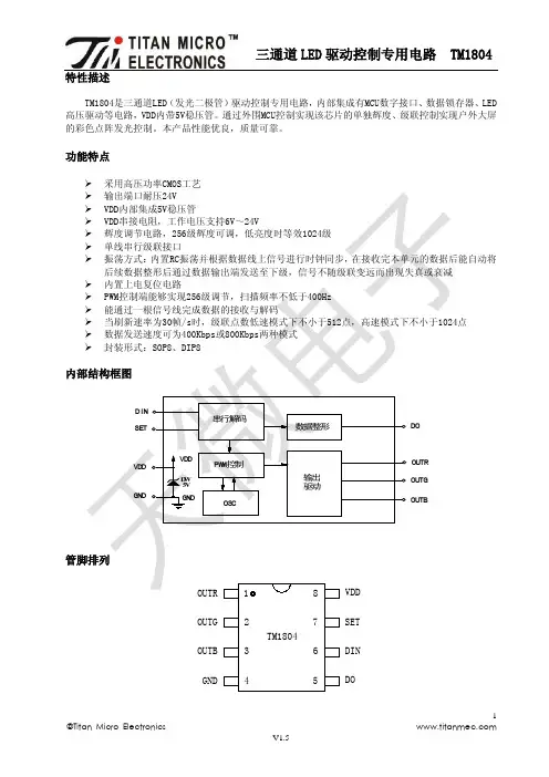
特性描述TM1804是三通道LED (发光二极管)驱动控制专用电路,内部集成有MCU 数字接口、数据锁存器、LED 高压驱动等电路,VDD 内带5V 稳压管。
通过外围MCU 控制实现该芯片的单独辉度、级联控制实现户外大屏的彩色点阵发光控制。
本产品性能优良,质量可靠。
功能特点采用高压功率CMOS 工艺 输出端口耐压24V VDD 内部集成5V 稳压管VDD 串接电阻,工作电压支持6V ~24V辉度调节电路,256级辉度可调,低亮度时等效1024级 单线串行级联接口 振荡方式:内置RC 振荡并根据数据线上信号进行时钟同步,在接收完本单元的数据后能自动将后续数据整形后通过数据输出端发送至下级,信号不随级联变远而出现失真或衰减 内置上电复位电路PWM 控制端能够实现256级调节,扫描频率不低于400Hz 能通过一根信号线完成数据的接收与解码当刷新速率为30帧/s 时,级联点数低速模式下不小于512点,高速模式下不小于1024点 数据发送速度可为400Kbps 或800Kbps 两种模式 封装形式:SOP8、DIP8内部结构框图GN DVD DDI NSE TGN DDOVD D串行解码数据整形PW M控制OS C输出驱动OU TR OU TG OU TBD W5V管脚排列453627SET18VDDGNDOUTB DODIN TM1804OUTG OUTR管脚功能引脚名称引脚序号I/O功能说明DIN 6 I 显示数据输入 DO 5 O 显示数据级联输出SET 7 - 接VDD :低速模式;悬空:高速模式OUTR 1 O Red PWM 控制输出 OUTG 2 O Green PWM 控制输出 OUTB 3 O Blue PWM 控制输出VDD 8 - DC 5V±10% GND4-接系统地输入输出等效电路VDDGNDDINVDD GND DOGNDOUTn SETVDD集成电路系静电敏感器件,在干燥季节或者干燥环境使用容易产生大量静电,静电放电可能会损坏集成电路,天微电子建议采取一切适当的集成电路预防处理措施,不正当的操作和焊接,可能会造成ESD 损坏或者性能下降,芯片无法正常工作。
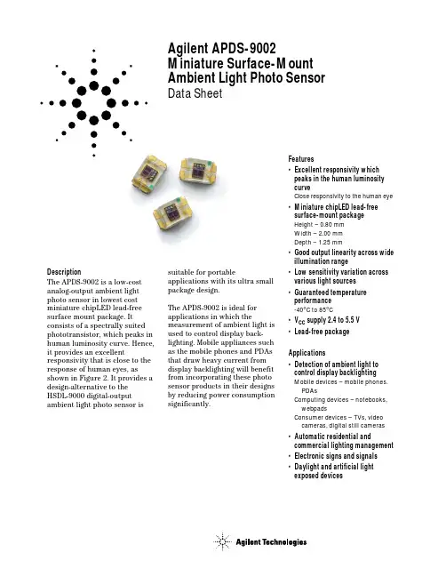
Agilent APDS-9002 Miniature Surface-Mount Ambient Light Photo Sensor Data SheetDescriptionThe APDS-9002 is a low-cost analog-output ambient light photo sensor in lowest cost miniature chipLED lead-free surface mount package. It consists of a spectrally suited phototransistor, which peaks in human luminosity curve. Hence, it provides an excellent responsivity that is close to the response of human eyes, as shown in Figure 2. It provides a design-alternative to theHSDL-9000 digital-output ambient light photo sensor is suitable for portableapplications with its ultra smallpackage design.The APDS-9002 is ideal forapplications in which themeasurement of ambient light isused to control display back-lighting. Mobile appliances suchas the mobile phones and PDAsthat draw heavy current fromdisplay backlighting will benefitfrom incorporating these photosensor products in their designsby reducing power consumptionsignificantly.Features•Excellent responsivity whichpeaks in the human luminositycurveClose responsivity to the human eye•Miniature chipLED lead-freesurface-mount packageHeight – 0.80mmWidth – 2.00mmDepth – 1.25mm•Good output linearity across wideillumination range•Low sensitivity variation acrossvarious light sources•Guaranteed temperatureperformance-40°C to 85°C•V CC supply 2.4 to 5.5V•Lead-free packageApplications•Detection of ambient light tocontrol display backlightingMobile devices – mobile phones,PDAsComputing devices – notebooks,webpadsConsumer devices – TVs, videocameras, digital still cameras•Automatic residential andcommercial lighting management•Electronic signs and signals•Daylight and artificial lightexposed devicesApplication Support InformationThe Application EngineeringGroup is available to assist youwith the application designassociated with APDS-9002ambient light photo sensormodule. You can contact themthrough your local salesrepresentatives for additionaldetails.Ordering InformationPart Number Packaging Type Package Quantity APDS-9002-021Tape and Reel4-pins Chipled package2500Typical Application CircuitFigure 1. Typical application circuit for APDS-9002.Figure 1 TableRecommended ApplicationComponent Circuit ComponentsR LOAD 1 k WI/O Pins Configuration TablePin Symbol Description1IOUT I OUT2VCC V CC3VCC V CC4NC No ConnectFigure 2. Relative spectral response vs. wavelength.CAUTIONS: It is advised that normal static precautions be taken in handling and assembly of this component to prevent damage and/or degradation which may be induced by ESD.Absolute Maximum RatingsFor implementations where case to ambient thermal resistance is ≤ 50°C/W ParameterSymbol Min.Max.Units Storage Temperature T S -4085°C Operating Temperature T A -4085°C Supply VoltageV CC2.45.5VRecommended Operating Conditions ParameterSymbol Min.Max.Units ConditionsOperating Temperature T A -4085°C Supply VoltageV CC2.45.5VN O R M A L I Z E D R E S P O N S I V I T YWAVELENGTH (nm)4500.56500.10.41.11.05501250115010509508507503500.70.20.30.60.90.8Electrical & Optical Specifications (T A = 25°C)Parameter Symbol Min.Typ.Max.Units ConditionsPhoto Current (I)I_PH1102033µA V CC = 3.0 V, Lux = 10[2]Photo Current (II)I_PH2136250410µA V CC = 3.0 V, Lux = 100[2]Photo Current (III)I_PH3-300-µA V CC = 3.0 V, Lux = 100[1]Dark Current I_DARK -50160nA V CC = 3.0 V, Lux = 0Light Current Ratio I_PH3 / I_PH2- 1.2---Rise Time T_RISE -0.952ms V CC = 3.0 V, Lux = 100, R load = 1 k Ω[3]Fall TimeT_FALL-0.82msV CC = 3.0 V, Lux = 100, R load = 1 k Ω[3]Notes:1.Illuminance by CIE standard light source (incandescent lamp).2.Fluorescent light is used as light source. White LED is substituted in mass production.3.White LED is used as light source.Light Measurement Circuit and WaveformsLOADPIN 2: VCC PIN 3: VCCFigure 3. Photocurrent vs. luminence (V CC = 3 V, T A = 25°C).Figure 4. Normalized photocurrent vs.temperature (V CC = 3 V, 100 LUX).Figure 5. Normalized photocurrent vs. angle (V CC = 3 V, T A = 25°C).Figure 6. Output voltage vs. luminance at different load resistor.Figure 7. Fall time vs. R LOAD .Figure 8. Rise time vs. R LOAD .LUXP H O T O C U R R E N T (A )0.010.0010.00010.00001TEMPERATURE (°C)N O R M A L I Z E D P H O T O C U R R E N TANGLEN O R M A L I Z E D P H O T O C U R R E N T0R LOAD (W )F A L L T IM E (s e c )000.0E+0200.0E-6400.0E-6600.0E-6800.0E-61.0E-31.2E-31.4E-3R LOAD (W )T r i s e (se c )000.0E+0200.0E-6400.0E-6600.0E-6800.0E-61.0E-31.2E-31.6E-31.4E-31.8E-3LUMINANCE, Ev (LUX)O U T P U T V O L T A G E , V O U T (V )1010.010.0010.1Moisture Proof PackagingAll APDS-9002 options are shipped in moisture proof package. Once opened, moisture absorption begins.This part is compliant to JEDEC Level 4.Baking ConditionsIf the parts are not stored in dry conditions, they must be baked before reflow to prevent damage to the parts.Package Temp.TimeIn Reels 60°C20 hours In Bulk125°C 5 hoursBaking should only be done once.Recommended Storage Conditions Storage Temperature10°C to 30°C Relative Humidity Below60% RHTime from Unsealing to Soldering After removal from the bag, the parts should be soldered within three days if stored at the recommended storage conditions. If times longer than three days are needed, the parts must be stored in a dry box.Recommended Reflow ProfileProcess Zone Symbol D TMaximum D T/D Time Heat Up P1, R125°C to 160°C 4°C/s Solder Paste Dry P2, R2160°C to 200°C0.5°C/s Solder Reflow P3, R3200°C to 255°C (260°C at 10 seconds max.)4°C/s P3, R4255°C to 200°C -6°C/s Cool DownP4, R5200°C to 25°C-6°C/sThe reflow profile is a straight-line representation of a nominal temperature profile for aconvective reflow solder process.The temperature profile is divided into four process zones, each with different D T/D time temperature change rates. The D T/D time rates are detailed in the above table.The temperatures are measured at the component to printed circuit board connections.In process zone P1, the PC board and APDS-9002 castellation pins are heated to a temperature of 160°C to activate the flux in the solder paste. The temperature ramp up rate, R1, is limited to 4°C per second to allow for evenheating of both the PC board and APDS-9002 castellations.Process zone P2 should be ofsufficient time duration (60 to 120seconds) to dry the solder paste.The temperature is raised to a level just below the liquidus point of the solder, usually 200°C (392°F).Process zone P3 is the solder reflow zone. In zone P3, the temperature is quickly raised above the liquidus point of solder to 255°C (491°F) for optimum results. The dwell time above the liquidus point of solder should be between 20 and 60 seconds. It usually takes about 20 seconds to assure proper coalescing of the solder balls into liquid solder and the formation of good solderconnections. Beyond a dwell time of 60 seconds, the intermetallicgrowth within the solderconnections becomes excessive,resulting in the formation of weak and unreliable connections. The temperature is then rapidly reduced to a point below thesolidus temperature of the solder,usually 200°C (392°F), to allow the solder within the connections to freeze solid.Process zone P4 is the cool down after solder freeze. The cool down rate, R5, from the liquidus point of the solder to 25°C (77°F)should not exceed 6°C per second maximum. This limitation is necessary to allow the PC board and APDS-9002 castellations to change dimensions evenly,putting minimal stresses on the APDS-9002.t-TIME (SECONDS)T – T E M P E R A T U R E – (°C )23020016012080180220255P1HEAT UPP2SOLDER PASTE DRYP3SOLDER REFLOWP4COOL DOWN25Appendix A: SMT Assembly Application NoteAgilent APDS-9002: Miniature Surface-Mount Ambient Light SensorFigure 9. Stencil and PCBA.1.1 Recommended Land PatternSOLDER MASKFigure 10. Solder stencil aperture.1.3 Adjacent Land Keepout and Solder Mask AreasAdjacent land keep-out is the maximum space occupied by the unit relative to the land pattern.There should be no other SMD components within this area.The minimum solder resist strip width required to avoid solder bridging adjacent pads is 0.2mm .Note: Wet/Liquid Photo-Imageable solder resist/mask is recommended.Figure 11. Adjacent land keepout and solder mask areas.1.2 Recommended Metal Solder Stencil ApertureIt is recommended that a 0.10 mm (0.004 inches) thick stencil be used for solder paste printing. Aperture opening for shield pad is 0.6 mm x 0.6 mm.This is to ensure adequateprinted solder paste volume and no shorting.Appendix B: Optical Window Design for APDS-90022.0Optical Window Dimensions To ensure that the performance of the APDS-9002 will not be affected by improper window design, there are some constraints on the dimensions and design of the window. There is a constraint on the minimum size of the window,which is placed in front of thephoto light sensor, so that it will not affect the angular response of the APDS-9002. This minimum dimension that is recommended will ensure at least a ±35° light reception cone.If a smaller window is required, a light pipe or light guide can be used. A light pipe or light guide is a cylindrical piece of transparent plastic, which makes use of total internal reflection to focus the light.The thickness of the window should be kept as minimum as possible because there is a loss of power in every optical window of about 8% due to reflection (4% on each side) and an additional loss of energy in the plastic material.Figures 12(a) and 12(b) illustrate the two types of windows that we have recommended which could either be a flat window or a flat window with light guide.Figure 12(a). Window size determination for flat window.Figure 12(b). Window design of flat window with light guide.FLATPHOTO LIGHT SENSORFigure 13. Recommended window dimensions.Table 1 and Figure 13 below show the recommended dimensions of the window. These dimension values are based on a window thickness of 1.0mm with a refractive index 1.585.Table 1: Recommended Dimension for Optical Window All dimensions are in mmFlat WindowFlat Window with Light Pipe WD(L = 0.0)(D2 = 1.5; Z = 0.5)(T+L+Z)Z D1D1L 1.50.5 2.25--2.0 1.0 3.25--2.5 1.5 4.25--3.0 2.0 5.00 2.5 1.5Table 2: Recommended Plastic Materials Material Number Visible Light Transmission Refractive Index Makrolon LQ264787% 1.587Makrolon LQ314787% 1.587Makrolon LQ318785%1.5872.1 Optical Window Material The material of the window isrecommended to be polycarbonate.The surface finish of the plastic should be smooth, without any texture.The recommended plastic material for use as a window is available from Bayer AG and Bayer Antwerp N. V. (Europe), Bayer Corp. (USA)and Bayer Polymers Co., Ltd.(Thailand), as shown in Table 2.The window should be placed directly on top of the photo light sensor to achieve better performance and if a flat window with a light pipe is used,dimension D2 should be 1.5 mm to optimize the performance ofAPDS-9002.PHOTO LIGHT SENSORZD1TOP VIEWD1WINDOW DIAMETER T THICKNESSL LENGTH OF LIGHT PIPEZDISTANCE BETWEEN WINDOW REAR PANEL AND APDS-9002Appendix C: General Application Guide for APDS-9002The APDS-9002 is a low cost analog-output ambient light photo sensor which spectral response closely emulates the human eyes. APDS-9002 consists of a phototransistor that enables the photo sensor to produce a high gain photo current to a sufficient level that can be converted to voltage with a standard value of external resistor. APDS-9002 is then easily integrated into systems that use ADC input which is available for sampling of the external source, as shown in Figure 14 below.Selection of the load resistor R L will determine the amount of current-to-voltage conversion in the circuit. Based on Figure 14 and using white LED as the light source, measurement has been carried out by using different load resistors to examine the variation of the output voltage towards the intense of LUX. The result is shown in Graph 1. APDS-9002 allows output voltage hits around 2.3 V, after this it saturates.Light source, e.g., fluorescent light, consists of ac noise about 100 Hz frequency. A capacitor of 10 µF, which acts as a low-pass filter, is recommended to add in parallel with resistor to by-pass the ripples.Figure 14. Configuration of APDS-9002 being used directly.The amount of converted voltage,V OUT, is mainly dependantproportionally on the photocurrent which is generated by thebrightness of the light shone onthe photo sensor and the loadresistor used, R L. Increasing thebrightness of the light and/or theload resistor will increase theoutput voltage.Brightness is measured as “LUX”unit, which describes how intensea light source that our eyesperceive. LUX meter is theequipment for “LUX”measurement. Light sources withthe same LUX level appear at thesame brightness to the humaneyes.Graph 1. Output voltage vs. luminance at different load resistor.V VLIGHTSOURCELUMINANCE, Ev (LUX)OUTPUTVOLTAGE,VOUT(V)1010.010.0011010010000.1Agilent has fabricated an evaluation board based on the configuration shown in Figure 14 for the designer to test the ambient light sensor under different lighting conditions. A reference layout of a 2-layout Agilent evaluation board for APDS-9002 is shown in Figure 15 below.Figure 15. Evaluation board layout./semiconductors For product information and a complete list of distributors, please go to our web site.For technical assistance call:Americas/Canada: +1 (800) 235-0312 or (916) 788-6763Europe: +49 (0) 6441 92460China: 10800 650 0017Hong Kong: (+65) 6756 2394India, Australia, New Zealand: (+65) 6755 1939 Japan: (+81 3) 3335-8152 (Domestic/Interna-tional), or 0120-61-1280 (Domestic Only) Korea: (+65) 6755 1989Singapore, Malaysia, Vietnam, Thailand, Philippines, Indonesia: (+65) 6755 2044 Taiwan: (+65) 6755 1843Data subject to change.Copyright © 2005 Agilent Technologies, Inc. May 10, 20055989-3051EN。
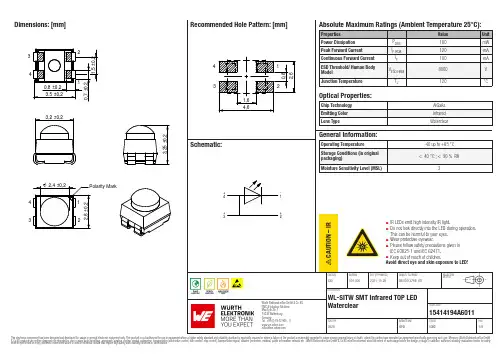
Dimensions: [mm]344315414194A601115414194A601115414194A601115414194A6011BC15414194A6011T e m p e r a t u r eT pT L15414194A6011Cautions and Warnings:The following conditions apply to all goods within the product series of Optoelectronic Components of Würth Elektronik eiSos GmbH & Co. KG:General:•This optoelectronic component is designed and manufactured for use in general electronic equipment.•Würth Elektronik must be asked for written approval (following the PPAP procedure) before incorporating the components into any equipment in fields such as military, aerospace, aviation, nuclear control, submarine, transportation (automotive control, train control, ship control), transportation signal, disaster prevention, medical, public information network, etc. where higher safety and reliability are especially required and/or if there is the possibility of direct damage or human injury.•Optoelectronic components that will be used in safety-critical or high-reliability applications, should be pre-evaluated by the customer. •The optoelectronic component is designed and manufactured to be used within the datasheet specified values. If the usage and operation conditions specified in the datasheet are not met, the wire insulation may be damaged or dissolved.•Do not drop or impact the components, the component may be damaged.•Würth Elektronik products are qualified according to international standards, which are listed in each product reliability report. Würth Elektronik does not warrant any customer qualified product characteristics beyond Würth Elektroniks’ specifications, for its validity and sustainability over time.•The responsibility for the applicability of the customer specific products and use in a particular customer design is always within the authority of the customer. All technical specifications for standard products also apply to customer specific products.•Unless Würth Elektroik has given its express consent, the customer is under no circumstances entitled to reverse engineer, disassemble or otherwise attempt to extract knowledge or design information from the optoelectronic component.Product specific:Soldering:•The solder profile must comply with the technical product specifications. All other profiles will void the warranty.•All other soldering methods are at the customers’ own risk.•The soldering pad pattern shown above is a general recommendation for the easy assembly of optoelectronic component. If a high degree of precision is required for the selected application (i.e. high density assembly), the customer must ensure that the soldering pad pattern is optimized accordingly.Cleaning and Washing:•Washing agents used during the production to clean the customer application might damage or change the characteristics of the optoelectronic component body, marking or plating. Washing agents may have a negative effect on the long-term functionality of the product. •Using a brush during the cleaning process may break the optoelectronic component body. Therefore, we do not recommend using a brush during the PCB cleaning process.Potting:•If the product is potted in the customer application, the potting material might shrink or expand during and after hardening. Shrinking could lead to an incomplete seal, allowing contaminants into the optoelectronic component body, pins or termination. Expansion could damage the components. We recommend a manual inspection after potting to avoid these effects.Storage Conditions:• A storage of Würth Elektronik products for longer than 12 months is not recommended. Within other effects, the terminals may suffer degradation, resulting in bad solderability. Therefore, all products shall be used within the period of 12 months based on the day of shipment.•Do not expose the optoelectronic component to direct sunlight.•The storage conditions in the original packaging are defined according to DIN EN 61760-2.•For a moisture sensitive component, the storage condition in the original packaging is defined according to IPC/JEDEC-J-STD-033. It is also recommended to return the optoelectronic component to the original moisture proof bag and reseal the moisture proof bag again. •The storage conditions stated in the original packaging apply to the storage time and not to the transportation time of the components. Packaging:•The packaging specifications apply only to purchase orders comprising whole packaging units. If the ordered quantity exceeds or is lower than the specified packaging unit, packaging in accordance with the packaging specifications cannot be ensured. Handling:•Violation of the technical product specifications such as exceeding the nominal rated current, will void the warranty.•The product design may influence the automatic optical inspection.•Certain optoelectronic component surfaces consist of soft material. Pressure on the top surface has to be handled carefully to prevent negative influence to the function and reliability of the optoelectronic components.•ESD prevention methods need to be applied for manual handling and processing by machinery.•Resistors for protection are obligatory.•Luminaires in operation may harm human vision or skin on a photo-biological level. Therefore direct light impact shall be avoided. •In addition to optoelectronic components testing, products incorporating these devices have to comply with the safety precautions given in IEC 60825-1, IEC 62471 and IEC 62778.•Please be aware that Products provided in bulk packaging may get bent and might lead to derivations from the mechanicalmanufacturing tolerances mentioned in our datasheet, which is not considered to be a material defect.Würth Elektronik eiSos GmbH & Co. KGEMC & Inductive SolutionsMax-Eyth-Str. 174638 WaldenburgGermanyCHECKED REVISION DATE (YYYY-MM-DD)GENERAL TOLERANCE PROJECTIONMETHODZAn001.0002021-10-26DIN ISO 2768-1mDESCRIPTIONWL-SITW SMT Infrared TOP LEDWaterclear ORDER CODE15414194A6011SIZE/TYPE BUSINESS UNIT STATUS PAGETechnical specification:•The typical and/or calculated values and graphics of technical parameters can only reflect statistical figures. The actual parameters of each single product, may differ from the typical and/or calculated values or the typical characteristic line.•On each reel, only one bin is sorted and taped. The bin is defined on intensity, chromaticity coordinate or wavelength and forward voltage.•In order to ensure highest availability, the reel binning of standard deliveries can vary. A single bin cannot be ordered. Please contact us in advance, if you need a particular bin sorting before placing your order.•Test conditions are measured at the typical current with pulse duration < 30ms. •Optical properties are measured according the CIE 127:2007 standard.•Wavelength tolerance under measurement conditions ± 2nm.•Optical intensity tolerance under measurement conditions ±15%.•Forward voltage tolerance under measurement conditions ± 0.1V.•CCT tolerance of x and y coordinate of ± 0.01and CRI tolerance of ± 2 is allowed In the characteristics curves, all values given in dotted lines may show a higher deviation than the parameters mentioned above.These cautions and warnings comply with the state of the scientific and technical knowledge and are believed to be accurate and reliable.However, no responsibility is assumed for inaccuracies or incompleteness.The customer has the sole responsibility to ensure that he uses the latest version of this datasheet, which is available on Würth Elektronik’s homepage. Unless otherwise agreed in writing (i.e. customer specific specification), changes to the content of this datasheet may occurwithout notice, provided that the changes do not have a significant effect on the usability of the optoelectronic componentsWürth Elektronik eiSos GmbH & Co. KG EMC & Inductive Solutions Max-Eyth-Str. 174638 Waldenburg GermanyCHECKED REVISION DATE (YYYY-MM-DD)GENERAL TOLERANCEPROJECTION METHODZAn001.0002021-10-26DIN ISO 2768-1mDESCRIPTIONWL-SITW SMT Infrared TOP LED WaterclearORDER CODE15414194A6011SIZE/TYPEBUSINESS UNITSTATUSPAGEImportant NotesThe following conditions apply to all goods within the product range of Würth Elektronik eiSos GmbH & Co. KG:1. General Customer ResponsibilitySome goods within the product range of Würth Elektronik eiSos GmbH & Co. KG contain statements regarding general suitability for certain application areas. These statements about suitability are based on our knowledge and experience of typical requirements concerning the areas, serve as general guidance and cannot be estimated as binding statements about the suitability for a customer application. The responsibility for the applicability and use in a particular customer design is always solely within the authority of the customer. Due to this fact it is up to the customer to evaluate, where appropriate to investigate and decide whether the device with the specific product characteristics described in the product specification is valid and suitable for the respective customer application or not.2. Customer Responsibility related to Specific, in particular Safety-Relevant ApplicationsIt has to be clearly pointed out that the possibility of a malfunction of electronic components or failure before the end of the usual lifetime cannot be completely eliminated in the current state of the art, even if the products are operated within the range of the specifications.In certain customer applications requiring a very high level of safety and especially in customer applications in which the malfunction or failure of an electronic component could endanger human life or health it must be ensured by most advanced technological aid of suitable design of the customer application that no injury or damage is caused to third parties in the event of malfunction or failure of an electronic component. Therefore, customer is cautioned to verify that data sheets are current before placing orders. The current data sheets can be downloaded at .3. Best Care and AttentionAny product-specific notes, cautions and warnings must be strictly observed. Any disregard will result in the loss of warranty.4. Customer Support for Product SpecificationsSome products within the product range may contain substances which are subject to restrictions in certain jurisdictions in order to serve specific technical requirements. Necessary information is available on request. In this case the field sales engineer or the internal sales person in charge should be contacted who will be happy to support in this matter.5. Product R&DDue to constant product improvement product specifications may change from time to time. As a standard reporting procedure of the Product Change Notification (PCN) according to the JEDEC-Standard inform about minor and major changes. In case of further queries regarding the PCN, the field sales engineer or the internal sales person in charge should be contacted. The basic responsibility of the customer as per Section 1 and 2 remains unaffected.6. Product Life CycleDue to technical progress and economical evaluation we also reserve the right to discontinue production and delivery of products. As a standard reporting procedure of the Product Termination Notification (PTN) according to the JEDEC-Standard we will inform at an early stage about inevitable product discontinuance. According to this we cannot guarantee that all products within our product range will always be available. Therefore it needs to be verified with the field sales engineer or the internal sales person in charge about the current product availability expectancy before or when the product for application design-in disposal is considered. The approach named above does not apply in the case of individual agreements deviating from the foregoing for customer-specific products.7. Property RightsAll the rights for contractual products produced by Würth Elektronik eiSos GmbH & Co. KG on the basis of ideas, development contracts as well as models or templates that are subject to copyright, patent or commercial protection supplied to the customer will remain with Würth Elektronik eiSos GmbH & Co. KG. Würth Elektronik eiSos GmbH & Co. KG does not warrant or represent that any license, either expressed or implied, is granted under any patent right, copyright, mask work right, or other intellectual property right relating to any combination, application, or process in which Würth Elektronik eiSos GmbH & Co. KG components or services are used.8. General Terms and ConditionsUnless otherwise agreed in individual contracts, all orders are subject to the current version of the “General Terms and Conditions of Würth Elektronik eiSos Group”, last version available at .Würth Elektronik eiSos GmbH & Co. KGEMC & Inductive SolutionsMax-Eyth-Str. 174638 WaldenburgGermanyCHECKED REVISION DATE (YYYY-MM-DD)GENERAL TOLERANCE PROJECTIONMETHODZAn001.0002021-10-26DIN ISO 2768-1mDESCRIPTIONWL-SITW SMT Infrared TOP LEDWaterclear ORDER CODE15414194A6011SIZE/TYPE BUSINESS UNIT STATUS PAGE。
SM2212EA订购信息若无特殊说明,环境温度为25°C。
注:表贴产品焊接最高峰值温度不能超过260℃,温度曲线依据J-STD-020 标准、参考工厂实际和锡膏商建议由工厂自行设定。
电气工作参数若无特殊说明,环境温度为25°C。
热阻参数注:芯片要焊接在有200mm2铜箔散热的PCB板,铜箔厚度35um。
SM2212EA 是可分段调光/调色温LED 恒流驱动控制电路,适用于200V~240V AC 输入电压,恒流精度小于±4%。
当SM2212EA 在分段调节亮度应用中,可根据开启关闭电源开关,依次改变输出电流的大小,从而改变LED 灯的亮度,调节比例可以通过外接REXT 电阻进行调整。
开关第一次开启 1rext R 0.61I =,开关第二次开启 2rext R 0.62I =,调光比例为100%,X%,2rext rext1R R %X =或X%,100%, 1rext rext2R R %X =。
当SM2212EA 在分段调节色温应用中,可根据开启关闭电源开关,依次改变两路输出端口开关状态,实现两路不同颜色LED 灯的交替亮灭以实现调节色温的目的,调节外接REXT 电阻可对系统输出功率进行调节。
芯片输出电流通过REXT 电阻进行调节。
开关第一次开启 1rext R 0.61I =,开关第二次开启 2rext R 0.62I =。
系统开关切换和复位时间描述SM2212EA 系统方案的开关切换时间由芯片VDD 端口控制,电容取值大小与复位时间关系曲线如下图1,建议取值1uF ,电容耐压值16V 。
SM2212EA 系统方案的复位时间由芯片VCC 端口控制,电容取值大小与复位时间关系曲线如下图2,建议取值4.7uF ,电容耐压值16V 。
图1 系统切换时间曲线图 图2 系统复位时间曲线图典型应用方案单颗芯片应用方案一高PF值调光方案L图3 SM2212EA 2段调光典型应用电路图典型应用:R1=10Ω,R2=100Ω,当0.3s<开关周期<3s:开关第一次开启时,OUT1端口启动,输出平均电流IOUT=30mA;开关第二次开启时,OUT2端口启动,输出平均电流IOUT=3mA;当开关周期>3s(VCC电容设置),回复初始状态,输出平均电流IOUT=30mA。
Product datasheetCharacteristicsTM200CE24Rcontroller M200 24 IO relay+EthernetMainRange of productEasy Modicon M200Product or component type Logic controller [Us] rated supply voltage 100...240 V AC Discrete I/O number 24Discrete input numberI2...I5: 4 fast inputI0, I1, I6, I7: 4 high speed input I8...I13: 6 regular input Discrete output number 10 relay Discrete input voltage 24 V Discrete input voltage type DCDiscrete input current 7 mA for inputDiscrete input logic Sink or source (positive/negative) type 1 conforming to EN/IEC 61131-2Discrete output voltage 24 V DC 220 V AC Discrete output current 2 ADiscrete output type Relay normally openPower consumption in VA52…64 VA at 100...240 V AC (with max I/O)ComplementaryMaximum number of I/O expansion module4 with 128 discrete output(s) for transistor output 4 with 74 discrete output(s) for relay output Supply voltage limits 85…264 V Network frequency 50/60 Hz Inrush current50 AVoltage state 1 guaranteed >= 15 V for input Voltage state 0 guaranteed <= 5 V for inputInput impedance 3.3 kOhm for discrete inputResponse time5 µs turn-off, I0, I1, I6, I7 terminal(s) for high speed input 5 µs turn-on, I0, I1, I6, I7 terminal(s) for high speed input 100 µs turn-off, I2...I5 terminal(s) for fast input 35 µs turn-on, I2...I5 terminal(s) for fast inputi s c l a i m e r : T h i s d o c u m e n t a t i o n i s n o t i n t e n d e d a s a s u b s t i t u t e f o r a n d i s n o t t o b e u s e d f o r d e t e r m i n i n g s u i t a b i l i t y o r r e l i a b i l i t y o f t h e s e p r o d u c t s f o r s p e c i f i c u s e r a p p l i c a t i o n s10 ms turn-off, Q0...Q9 terminal(s) for relay output10 ms turn-on, Q0...Q9 terminal(s) for relay output100 µs turn-off, I8...I13 terminal(s) for regular input35 µs turn-on, I8...I13 terminal(s) for regular inputConfigurable filtering time0 ms for input3 ms for input12 ms for inputOutput voltage limits30 V DC250 V ACMaximum current per output common4 A at COM 24 A at COM 04 A at COM 1Electrical durability100000 cycles AC-12, 240 V, 480 VA, resistive100000 cycles DC-12, 24 V, 48 W, resistiveSwitching frequency0.1 Hz with maximum loadMechanical durability20000000 cycles for relay outputMinimum load10 mA at 5 V DC for relay outputMemory capacity512 byte internal flash for backup of programsData storage equipment32 GB micro SD card (optional)Battery type BR2032 Li-CFx (Lithium-Carbon Monofluoride), battery life: 5 year(s)Backup time 3 years at 25 °C (by interruption of power supply)Execution time for 1 KInstruction0.3 ms for event and periodic taskExecution time per instruction0.2 µs BooleanExct time for event task60 µs response timeClock drift<= 90 s/month at 25 °CRegulation loop Adjustable PID regulator up to 14 simultaneous loopsControl signal type Quadrature (x1, x2, x4) at 100 kHz for fast input (HSC mode)Pulse/direction at 100 kHz for fast input (HSC mode)Single phase at 100 kHz for fast input (HSC mode)CW/CCW at 100 kHz for fast input (HSC mode)Counting input number 4 fast input (HSC mode) at 100 kHz 32 bitsIntegrated connection type USB port with mini B USB 2.0 connectorNon isolated serial link serial 1 with terminal block connector and RS485 interfaceNon isolated serial link serial 2 with terminal block connector and RS232/RS485 interfaceEthernet Modbus TCP/IP Ethernet with RJ45 connector and 1 Ethernet port 10/100BASE-T interfaceIsolated serial link serial 2 with terminal block connector and RS485 interfaceTransmission rate 1.2...115.2 kbit/s (115.2 kbit/s by default) for bus length of 15 m for RS4851.2...115.2 kbit/s (115.2 kbit/s by default) for bus length of 3 m for RS23212 Mbit/s for USB10/100 Mbit/s for bus length of 100 m for Ethernet Modbus TCP/IPCommunication port protocol USB port: USB - SoMachine-NetworkNon isolated serial link: Modbus master/slave - RTU/ASCII or SoMachine-NetworkEthernet Modbus TCP/IP: Modbus TCP/IP client/serverLocal signalling 1 LED (green)PWR:1 LED (green)RUN:1 LED (red)module error (ERR):1 LED (green)SD card access (SD):1 LED (red)BAT:1 LED (green)SL1:1 LED per channel (green)I/O state:2 LEDs (green)communication (LK/ACT 10/100):Electrical connection Mini B USB 2.0 connectorfor a programming terminalRJ45 connectorfor connecting Ethernet networkremovable screw terminal blockfor inputsremovable screw terminal blockfor outputsremovable screw terminal block, 4 terminal(s) for connecting the serial link1removable screw terminal block, 3 terminal(s) for connecting the 100-240 V AC power supplyMaximum cable distance between devices Unshielded cable: <50 m for input Shielded cable: <10 m for fast input Shielded cable: <10 m for high speed input Unshielded cable: <150 m for outputInsulation Non-insulated between inputsBetween output and internal logic at 1780 V ACBetween output groups at 1780 V ACBetween supply and internal logic at 1780 V ACBetween input and internal logic at 500 V ACBetween fast input and internal logic at 500 V ACBetween input groups at 500 V ACSensor power supply24 V DC at 250 mA supplied by the controllerMarking CEMounting support Top hat type TH35-15 rail conforming to IEC 60715Top hat type TH35-7.5 plate or panel with fixing kit conforming to IEC 60715Height90 mmDepth70 mmWidth130 mmProduct weight0.413 kgEnvironmentIP degree of protection IP20 with protective cover in placeProduct certifications RCMIACS E10CULusCSAStandards EN/IEC 61010-2-201EN/IEC 61131-2Electromagnetic compatibility Electrostatic discharge immunity test - test level: 8 kV (air discharge) conforming to EN/IEC61000-4-2Electrostatic discharge immunity test - test level: 6 kV (contact discharge) conforming to EN/IEC61000-4-2Susceptibility to electromagnetic fields - test level: 10 V/m (80 MHz...3 GHz) conforming to EN/IEC61000-4-3Magnetic field at power frequency - test level: 30 A/m conforming to EN/IEC 61000-4-8Electrical fast transient/burst immunity test - test level: 2 kV (power lines) conforming to EN/IEC61000-4-4Electrical fast transient/burst immunity test - test level: 2 kV (relay output) conforming to EN/IEC61000-4-4Electrical fast transient/burst immunity test - test level: 1 kV (I/O) conforming to EN/IEC 61000-4-4Electrical fast transient/burst immunity test - test level: 1 kV (serial link) conforming to EN/IEC61000-4-41.2/50 µs shock waves immunity test - test level: 1 kV (power lines (DC)) conforming to EN/IEC61000-4-51.2/50 µs shock waves immunity test - test level: 2 kV (power lines (AC)) conforming to EN/IEC61000-4-51.2/50 µs shock waves immunity test - test level: 2 kV (relay output) conforming to EN/IEC 61000-4-51.2/50 µs shock waves immunity test - test level: 1 kV (I/O) conforming to EN/IEC 61000-4-51.2/50 µs shock waves immunity test - test level: 1 kV (shielded cable) conforming to EN/IEC61000-4-51.2/50 µs shock waves immunity test - test level: 0.5 kV (power lines (DC)) conforming to EN/IEC61000-4-51.2/50 µs shock waves immunity test - test level: 1 kV (power lines (AC)) conforming to EN/IEC61000-4-5Conducted RF disturbances - test level: 10 V (0.15...80 MHz) conforming to EN/IEC 61000-4-6Conducted emission - test level: 79 dBμV/m QP/66 dBμV/m AV (power lines (AC)) conforming to EN/IEC 55011Conducted emission - test level: 73 dBμV/m QP/60 dBμV/m AV (power lines (AC)) conforming to EN/IEC 55011Radiated emission - test level: 40 dBμV/m QP class A (10 m) conforming to EN/IEC 55011Radiated emission - test level: 47 dBμV/m QP class A (10 m) conforming to EN/IEC 55011Electrical fast transient/burst immunity test - test level: 1 kV (Ethernet line) conforming to EN/IEC61000-4-4Shock resistance15 gn for 11 ms30 gn for 6 msImmunity to microbreaks10 msVibration resistance 3.5 mm at 5…8.4 Hz on symmetrical rail1 gn at 8.4…150 Hz on symmetrical rail3.5 mm at 5…8.7 Hz on panel mounting2 gn at 8.7…150 Hz on panel mountingRelative humidity10…95 %, without condensation (in operation)10…95 %, without condensation (in storage)Ambient air temperature for operation0…55 °C (horizontal installation)Ambient air temperature for storage-25…70 °CPollution degree<= 2Operating altitude0...2000 mStorage altitude0…3000 mOffer SustainabilitySustainable offer status Green Premium productEU RoHS Directive Pro-active compliance (Product out of EU RoHS legal scope)EU RoHS DeclarationMercury free YesRoHS exemption information YesChina RoHS Regulation China RoHS declarationEnvironmental Disclosure Product Environmental ProfileCircularity Profile End of Life InformationWEEE The product must be disposed on European Union markets following specific waste collection andnever end up in rubbish binsDimensions DrawingsDimensions Drawings DimensionsMounting and ClearanceMounting and Clearance Mounting on a RailDirect Mounting on a Panel SurfaceMounting PositionClearanceTMCR2•••InstallationTMCR2••• De-InstallationProduct datasheetTM200CE24R Connections and SchemaWiring Diagram / Connections SchemaAC Power Supply(*)Type T fuseDigital Inputs Positive Logic (Sink)(*)Type T fuse(**)Fast inputs(1)The COM0 and COM1 terminals are not connected internally.Digital Inputs Negative Logic (Source)(*)Type T fuse(**)Fast inputs(1)The COM0 and COM1 terminals are not connected internally.Relay Outputs - Negative Logic (Sink)(*)Type T fuse(1)The COM0 and COM1 terminals are not connected internally.(2) A free wheeling diode or an RC snubberRelay Outputs - Positive Logic (Source)(*)Type T fuse(1)The COM0 and COM1 terminals are not connected internally.(2) A free wheeling diode or an RC snubberEthernet ConnectionUSB Mini-B ConnectionSL1 ConnectionD1 :D1 (A+)D0 :D0 (B-)Shield :ShieldCOM :O V ComProduct datasheetTM200CE24R Performance CurvesDerating CurvesDigital InputsX :Ambient temperature (°C / °F)Y :Input voltage (V)。
UniOhm Uniroyal Electronics Industry Co., Ltd.厚声电子工业有限公司88 LongTeng Road, Economic & Technical Development Zone,Kunshan City, Jiangsu, China中国江苏省昆山市经济技术开发区龙腾路88号邮编: 215301Tel: +86 512 5763 1400 / 1411 /1422 /1433Fax: +86 512 5763 4599*******************************************Contents目录Metal Strip Current Sensing Chip Resistors - MS 金属带电流检测片式电阻器22MS06, MS07, MS10, MS11, MS12, MS17, MS20, MS27Anti-Electro Static Discharge Thick Film Chip Resistors - ES 抗静电膜晶片电阻器24ES01, ES02, ES03, ES05, ES06, ES07Low T.C.R Thick Film Chip Resistors - LT 低温度系数厚膜晶片电阻器26LT02, LT03, LT05, LT06AEC-Q200 Version Chip Resistors - HQ 汽车用晶片电阻器28HQ02, HQ03, HQ05, HQ06, HQ07, HQ10 , HQ12Thick Film Chip Resistors Network 厚膜晶片网络电阻器4610P8, 10S8, 10T8, 10E9Packing of Surface Mount Resistors 表面贴装式电阻器包装47Packing of Surface Mount ResistorsResistor Network - SIP Series 网络电阻器 - SIP 系列48RNL-A, RNL-B, RNL-C, RNL-D, RNL-E, RNL-L, RNL-R,RNL-G, RNL-PHigh Power Resistor Network - SIP RPL Series 高功率网络电阻器- SIP RPL 系列50RPL-A, RPL-B, RPL-RHigh Power Resistors Network Medium Profile–SIP RNM Series高功率中宽度网络电阻器 - SIP RNM 系列52RNM-A, RNM-B, RNM-RHigh Power Resistors Network High Profile–SIP RPH Series高功率高宽度网络电阻器 - SIP RPH 系列54RPH-A, RPH-B, RPH-RSpecial Network –SIP Series 特殊网络电阻器 - SIP 系列56SN0001, SN0002, SN0003, SN0004Resistor/Capacitor Network-SIP Series 网络阻容器电阻器 - SIP 系列57RCN-A, RCN-BCapacitor Network-SIP Series 网络电容器 - SIP 系列58CNM-1High Voltage Flat Resistors 高压扁平式电阻器59HFRCarbon Film Fixed Resistors 碳膜电阻器60CFRPrecision Metal Film Fixed Resistors 精密金属膜电阻器62MFRCarbon Film Power Resistors 高功率碳膜电阻器64CPR Metal Film Power Resistors 高功率金属膜电阻器65MPRWire-wound Fusible Resistors 绕线保险丝型电阻器74KFRThermal Fusing Wire-wound Fixed Resistors 绕线型温度保险丝电阻器76TFRCurrent Sense Resistors 电流检测线电阻器77CSRCurrent Sense Spring Resistors 弹簧式电流检测电阻器78CSSA, CSSB, CSSCThrough Hole Category - Network Resistors & Traditional Coated Resistors (插件式 - 排列电阻 & 涂装型电阻)New New New New UniOhm1Contents目录Axial Leaded Terminal Type-PRW Series 轴式导线型 - PRW 系列 97PRW , PRWA, PRWCRadial Leaded T ype-PRM & PRS Series 立式导线型 - PRM & PRS 系列 98PRM, PRMA, PRMB, PRMT , PRSUltra-Low Value Cement Resistors 超低阻水泥固定电阻器108PRWUPower Flat Alloy Resistors 功率型合金箔电阻器109PFAS, PFATColumnar Type Cement Fixed Resistors 圆柱状水泥电阻器111QHOStandard Packing of Cement Type Resistors 水泥型电阻器包装标准112Bulk/BoxPower Dissipation Mount Resistors 铝外壳电阻器115PDMHigh-Power Wire-wound Resistors 高功率绕线型固定电阻器116BTRVitreous Enameled Wire-wound Resistors 珐琅釉绕线固定电阻器127URXPower Type Thermal Fusing Resistors 功率型温度保险丝电阻128TFO, TFRCPower (Ribbon) Wire-wound Resistors 功率(合金带)绕线型电阻器129QH, QL, QR, QRZGTest Method of JIS-C-5201 & JIS-C-5202JIS-C-5201和 JIS-C-5202 检测方法131Standard Nominal Resistance Value 标准电阻值133Explnation of Part No. System 料号系统注释135Standard Color Code System 标准色码系统137Metal Glaze Film Fixed Resistors 金属玻璃釉膜固定电阻器79MGRHigh-Value Metal Glaze Film Fixed Resistors 超高阻玻璃釉膜固定电阻器81HMGRHigh-Voltage Metal Glaze Film Fixed Resistors 耐高压型玻璃釉膜固定电阻器82HVRTerminal Type Metal Oxide Film Resistors 端片型金属氧化膜电阻器83TMOR, TMOV , TMOLJumper Wires & Zero-Ohm Resistors 跳线及零欧姆电阻器84ZW , ZO, ZFCopper Plated Steel Lead Wire Type & Cutting Type 铜包钢导线型及切割半成品型85CP, CO Panasert Type (Panasert 型)86Avisert Type (Avisert 型)87AVI-1, AVI-2, AVI-3M & F Forming Type (M 型 & F 型 <成型> )89MF , MK, ML, F , F1, F2, F3Standard Packing of Coated Type Resistors 涂装型电阻器包装标准91Tape/Box, Tape/Reel, Bulk/BoxThrough Hole Category - Traditional Cement Resistors (插件式 - 水泥型电阻)Power Type Resistors (功率型)RELATIVE INFORMATION (相关资料)UniOhm2• Small size & light weight 短小轻薄• Reduction of assembly costs and matching with placement machine. 可降低装置成本及配合机器组装• Suitable for both wave & re-flow soldering. 适合波峰焊与回流焊• Applications: Navigator (GPS), Mobile Phone,Telecom, PDA, Setbox, Meter.应用于GPS, 移动电话,PDA,机顶盒,仪表Feature (特性)Figures (型状)Derating Curve & Specification降功率曲线及性能Thick Film Chip ResistorsPercentratedload(%)Ambient termperature 环境温度 (°C)厚膜晶片电阻器负载比率(%)UniOhm3 RoHS CompliantValue阻值Code 代码Value 阻值Code 代码Value 阻值Code 代码Value 阻值Code 代码Value 阻值Code 代码Value 阻值Code 代码100011471721533316494646568181102021501822134324504756669882105031541922635332514876771583107041582023236340524996873284110051622123737348535116975085113061652224338357545237076886115071692324939365555367178787118081742425540374565497280688121091782526141383575627382589124101822626742392585767484590127111872727443402595907586691130121912828044412606047688792133131962928745422616197790993137142003029446432626347893194140152053130147442636497995395143162103230948453646658097696Thick Film Chip Resistors• For 01005, 0201, 0402 size, no marking on the body due to the small size of the resistor. 01005, 0201, 0402因电阻本体太小,故本体无标示字码• ±5% tolerance product: the marking is 3 digits, the first 2 digits are the significant of theresistance and the 3rd digit denotes number of zeros following.±5%公差产品字码是三位数,前二位是阻值的有效数,第三位表示有几个 0• 0805, 1206, 1210, 2010, 2512 ≤±1%: the marking is 4 digits, the first 3 digits are the significant of the resistance and the 4th digit denotes number of zeros following. 0805, 1206, 1210, 2010, 2512 ≤±1%公差产品字码有四位数,前三位是阻值的有效数,第四位表示有几个 0Marking on the Resistors Body (电阻本体字码标示)2372 = 23700Ω = 23.7KΩBelow 10Ω : 3R24 = 3.24Ω10Ω 以下标示: 3R24 = 3.24Ω153 = 15000Ω = 15KΩBelow 10Ω: 6R8 = 6.8Ω10Ω 以下标示: 6R8 = 6.8Ω• Standard E-96 series values of 0603 ≤±1%: due to the small size of the resistor’s body, 3 digits marking will be used to indicate the accurate resistance value by using the following Multiplier & Resistance Code. 0603 ≤±1%公差 E-96系列标准阻值,因电阻本体太小,采用三位阻值代码(数字)及下列指数代码(字母)配合来指明标准的阻值。
深圳金仕盾照明科技有限公司Shenzhen Jinsdon Lighting Technology Co.,Ltd产品规格书产品型号:JWL-LED文件编号:版本编号:V1.6发行日期:2013-01-08制定审核批准目录1产品规格 (3)1.1产品图片 (3)1.2应用领域 (3)1.3基本参数 (3)1.4产品型号识别 (4)1.5主要特点 (4)1.6详细参数 (5)1.7保护功能 (5)1.8状态指示 (6)1.9工作模式表 (7)1.10尺寸大小 (8)1.11重量 (8)2接线方式 (8)2.1接线和安装 (8)2.2LED负载连接 (9)2.3安装的时候如何判断整个系统是是否正常 (9)2.4如何检测JWL-LED恒流太阳能控制器是否有问题 (10)3典型性能图表 (11)3.1LED串联数目同效率及电流关系图1(电流300mA) (11)3.2LED串联数目同效率及电流关系图2(电流600mA) (11)3.3LED并联数目同效率关系 (12)3.4输出功率比与效率关系 (12)3.5温度同效率及电流的关系 (13)1.1产品图片1.2应用领域◇太阳能LED路灯◇太阳能LED庭院灯1.3基本参数1.蓄电池输入电压:12V/24V2.光电池输入电压:<55V3.光电池输入功率:≤170W/12V、≤340W/24V4.负载输出电流:30mA~ 1.5A5.最大输出功率:40W/12V;60W/24V6.待机静态功耗:3mA/12V、5mA/24V1.4产品型号识别JWL-LEDJWL:金仕盾防水控制器LED:LED专用控制器1.5主要特点◆内置高精度升压型恒流源,无需另配LED恒流源,单串最多可驱动14颗串联LED,可做5组并联;◆采用先进的Two-Phase Boost电路,保证了其高效率和高可靠性。
◆12V系统时恒流效率高达95%,24V系统效率高达96%;◆可四时段调光(即第一、二、三时段、天亮前开灯),调光时间自由设置;◆可自由调光的功率范围:10%-90%;◆可同时兼容12V系统与24V系统;◆延时开灯时间可调;◆具有过充、过放、电子短路、过载保护、独特的防反接保护;◆自主研制的散热器,散热性能优越,美观、实用。
集成电路布图设计专有权公告(2014年1月3日)布图设计登记号:BS.135011957布图设计申请日:2013年09月30日公告日期:2014年1月3日公告号:8421布图设计名称:FM24C512D布图设计类别:结构:MOS技术:CMOS功能:逻辑布图设计权利人:上海复旦微电子集团股份有限公司布图设计权利人国籍/省市:上海布图设计权利人地址:上海市国泰路127号4号楼布图设计创作人:上海复旦微电子集团股份有限公司布图设计创作完成日:2013年09月16日布图设计登记号:BS.135011965布图设计申请日:2013年09月30日公告日期:2014年1月3日公告号:8422布图设计名称:S55ADC布图设计类别:结构:MOS技术:CMOS功能:线性布图设计权利人:上海硅知识产权交易中心有限公司布图设计权利人国籍/省市:上海布图设计权利人地址:上海市徐汇区宜山路333号1704布图设计共同权利人:上海斯派克斯科技有限公司布图设计共同权利人国籍/省市:上海布图设计共同权利人地址:上海市张江科技园郭守敬路498号14幢22301-1450 布图设计创作人:徐步陆、邵博闻、林霞、俞慧月、刘芸、朱小峰、叶枝灿布图设计创作完成日:2012年06月05日布图设计登记号:BS.135011973布图设计申请日:2013年09月30日公告日期:2014年1月3日公告号:8423布图设计名称:高精度原边反馈LED恒流控制芯片RM3290布图设计类别:结构:MOS技术:CMOS功能:线性布图设计权利人:陕西亚成微电子股份有限公司布图设计权利人国籍/省市:西安布图设计权利人地址:西安市高新三路9号信息港大厦105室布图设计创作人:陕西亚成微电子股份有限公司布图设计创作完成日:2013年06月07日布图设计首次商业利用日:2013年09月13日布图设计登记号:BS.135011981布图设计申请日:2013年09月30日公告日期:2014年1月3日公告号:8424布图设计名称:单通道LED恒流驱动控制芯片RM9002布图设计类别:结构:MOS技术:CMOS功能:线性布图设计权利人:陕西亚成微电子股份有限公司布图设计权利人国籍/省市:西安布图设计权利人地址:西安市高新三路9号信息港大厦105室布图设计创作人:陕西亚成微电子股份有限公司布图设计创作完成日:2012年11月15日布图设计首次商业利用日:2013年07月15日布图设计登记号:BS.13501199X布图设计申请日:2013年09月30日公告日期:2014年1月3日公告号:8425布图设计名称:高功率高精度LED驱动芯片RM9110布图设计类别:结构:MOS技术:CMOS功能:线性布图设计权利人:陕西亚成微电子股份有限公司布图设计权利人国籍/省市:西安布图设计权利人地址:西安市高新三路9号信息港大厦105室布图设计创作人:陕西亚成微电子股份有限公司布图设计创作完成日:2013年07月30日布图设计首次商业利用日:2013年09月20日布图设计登记号:BS.135012031布图设计申请日:2013年10月09日公告日期:2014年1月3日公告号:8426布图设计名称:YYS32F201集成电路布图设计布图设计类别:结构:Bi-MOS技术:CMOS功能:其他布图设计权利人:徐惟布图设计权利人国籍/省市:上海布图设计权利人地址:上海市天雄路588弄3号楼布图设计创作人:徐惟布图设计创作完成日:2013年09月16日布图设计登记号:BS.13501204X布图设计申请日:2013年10月01日公告日期:2014年1月3日公告号:8427布图设计名称:HY029布图设计类别:结构:MOS技术:CMOS功能:逻辑布图设计权利人:无锡汉咏微电子有限公司布图设计权利人国籍/省市:江苏布图设计权利人地址:江苏省无锡市新区长江路21-1号国家IC设计基地207-2 布图设计创作人:韩基东、郑云华、朱舰、吴彩虹代理机构:无锡市大为专利商标事务所代理人:殷红梅布图设计创作完成日:2013年04月18日布图设计首次商业利用日:2013年08月01日布图设计登记号:BS.135012058布图设计申请日:2013年09月26日公告日期:2014年1月3日公告号:8428布图设计名称:激光控制电路808Rev.B布图设计类别:结构:Bi-MOS技术:IIL功能:微型计算机布图设计权利人:上海法诺光电技术有限公司布图设计权利人国籍/省市:上海布图设计权利人地址:上海市普陀区怒江北路449弄8号1幢2楼布图设计创作人:颜小琴代理机构:上海精晟知识产权代理有限公司代理人:冯子玲布图设计创作完成日:2013年04月09日布图设计登记号:BS.135012066布图设计申请日:2013年09月26日公告日期:2014年1月3日公告号:8429布图设计名称:光子控制电路TM990A-MRev.D布图设计类别:结构:Bi-MOS技术:IIL功能:微型计算机布图设计权利人:上海法诺光电技术有限公司布图设计权利人国籍/省市:上海布图设计权利人地址:上海市普陀区怒江北路449弄8号1幢2楼布图设计创作人:颜小琴代理机构:上海精晟知识产权代理有限公司代理人:冯子玲布图设计创作完成日:2012年03月06日布图设计登记号:BS.135012074布图设计申请日:2013年09月26日公告日期:2014年1月3日公告号:8430布图设计名称:光子射频控制电路1-VL002-090827-V2.0-1T布图设计类别:结构:Bi-MOS技术:IIL功能:微型计算机布图设计权利人:颜小琴布图设计权利人国籍/省市:上海布图设计权利人地址:上海市普陀区怒江北路449弄8号1幢2楼布图设计创作人:颜小琴代理机构:上海精晟知识产权代理有限公司代理人:冯子玲布图设计创作完成日:2012年06月08日布图设计登记号:BS.135012082布图设计申请日:2013年10月10日公告日期:2014年1月3日公告号:8431布图设计名称:CASAGEM 芯片布图设计类别:结构:MOS技术:CMOS功能:线性布图设计权利人:清华大学布图设计权利人国籍/省市:北京布图设计权利人地址:北京市100084-82信箱布图设计创作人:何力代理机构:北京众合诚成知识产权代理有限公司代理人:薄观玖布图设计创作完成日:2011年12月06日布图设计首次商业利用日:2013年09月25日布图设计登记号:BS.135012090布图设计申请日:2013年10月10日公告日期:2014年1月3日公告号:8432布图设计名称:FM24NC128布图设计类别:结构:MOS技术:CMOS功能:存储布图设计权利人:上海复旦微电子集团股份有限公司布图设计权利人国籍/省市:上海布图设计权利人地址:上海市国泰路127号4号楼布图设计创作人:上海复旦微电子集团股份有限公司布图设计创作完成日:2013年10月08日。
SM16159概述SM16159是LED 高密全彩屏专用驱动芯片,内置16K 的SRAM 存储结构,能够存储一帧完整显示数据,支持1~32扫LED 显示屏整帧数据存储及显示。
此方式降低了数据时钟频率,并可实现高灰阶效果。
SM16159内建16位灰阶控制的脉冲宽度调变功能,16个恒流输出通道所输出的电流值不受输出端负载电压的影响并提供一致且恒定的输出电流。
可通过选用外接电阻或调节6位电流增益来调整整体LED 的驱动电流。
封装信息特点◆ 内置64级电流增益调节功能 ◆ 内置16k SRAM ,支持1~32扫 ◆ 行扫倍频技术,刷新率提升2/4/8倍◆ 内置开路检测功能,解决开路“十字架”问题 ◆ 内置列下消影功能◆ 内置偏色、低灰麻点、第一扫偏暗改善功能 ◆ 16位PWM 灰阶控制可调显示刷新率SM_PWM专利技术◆ 工作电压:3.3V~5.0V◆ 输出恒流范围:0.6~32mA@VDD=5.0V ;0.6~24mA@VDD=3.3V ◆ 输出电流精度:通道间偏差:<±2.0%(最大值) 芯片间偏差:<±2.5%(最大值)管脚定义111213141516171819202122231098765432124OUT4OUT3OUT5OUT6OUT7OUT2OUT1OUT0LE DCLK SDI GND OUT8OUT9OUT10OUT11OUT12OUT13OUT14OUT15GCLK SDO REXT VDDS D ID DE X TD OC L KO U T OUT3OUT2OUT1OUT0LE OUT4C L KO U T G N DO U T O U T O U T内部功能框图LESDISDO管脚说明订购信息输出及输入等效电路GCLK,DCLK,SDI输入端LE输入端SDO输出端最大限定范围静态特性(V静态特性(V动态特性(V动态特性(V*在时序波形图(1)中,LE下降延后SDO的输出变化。