LED恒流驱动MY9366规格书
- 格式:pdf
- 大小:1013.84 KB
- 文档页数:5
TM1642是一种带键盘扫描接口的恒流LED(发光二极管显示器)驱动控制专用电路,内部集成有MCU 数字接口、数据锁存器、LED 高压驱动、键盘扫描等电路。
本产品性能优良,质量可靠。
主要应用于段码LED产品的恒流显示屏驱动。
采用SOP28的封装形式。
功能特点•采用功率CMOS 工艺•多种显示模式(10段×7位~13段×4位)•SEG 恒流驱动最大电压值:VDD-1V •通道差最大+/-3%芯片间最大+/-6%•键扫描(8×2)•辉度调节电路(软件8级恒流可调)•串行接口(CLK,STB,DIN)•振荡方式:内置RC 振荡(450KHz+5%)•内置上电复位电路•封装形式:SOP28管脚信息123456789101112131415161718192021222324TM1642NCDINCLK STB K1K2VDDSEG1/KS1SEG2/KS2SEG3/KS3SEG4/KS4SEG5/KS5SEG6/KS6SEG7/KS7SEG8/KS8SEG9SEG10GRID1GRID2GRID3GRID4SEG14/GRID5SEG13/GRID SEG12/GRID VDD GND GND GND 25262728TOP VIEWSOP28深圳市富瑞世嘉科技有限公司13530167943天微专营为高时,CLK 被忽略输入该脚的数据在显示周期结束后被锁存段恒流输出(也用作键扫描),p管开漏输出16~17段恒流输出,P管开漏输出27、2624、23位输出,N管开漏输出输出(段/位)18~20段/位复用输出,只能选段或位输出逻辑电源7、215V±10%逻辑地22、25、28接系统地▲注意:DIN口输出数据时为N管开漏输出,在读键的时候需要外接1K-10K的上拉电阻,如图(1)所示。
本公司推荐10K的上拉电阻。
DOUT在时钟的下降沿控制N管的动作,此时读数不稳定,可以参考图(4),在时钟的上升沿时读数才稳定。
MYD-Y6ULX 产品数据手册版本V1.02017.10.20版本记录版本号说明时间V1.0初始版本2017.10.20目录目录 (3)第1章概述 (5)第2章硬件参数 (8)2.1核心板硬件资源 (8)2.2底板硬件资源 (8)第3章接口说明 (11)3.1核心板接口说明 (11)3.1底板接口说明 (11)第4章硬件设计 (14)4.1核心板硬件电路设计 (14)4.2底板硬件电路设计 (14)4.2.1电源 (14)4.2.2启动位配置开关 (15)4.2.3以太网 (16)4.2.4USB (17)4.2.5LTE模块 (19)4.2.6Audio (20)4.2.7WIFI (21)4.2.8Camera (22)4.2.9LCD (23)4.2.10UART (24)4.2.11CAN (25)4.2.12RTC备份电池 (26)4.2.13Micro SD (27)4.2.14Key and LED (27)4.2.15扩展接口 (28)第5章电气参数 (30)5.1工作温度 (30)5.2GPIO直流特性 (30)5.3电源直流特性 (30)第6章机械参数 (32)附录一联系方式 (34)附录二售后服务与技术支持 (35)第1章概述MYD-Y6ULX是米尔科技推出的基于NXP公司i.MX6UL/6ULL系列处理器的嵌入式开发板。
i.MX6UL是一个高功效、高性价比的应用处理器系列,采用单个ARM Cortex-A7内核,运行速度高达696MHz。
i.MX6ULL在i.MX6UL的基础上精简了安全加密部分,但主频最高可达900MHz,更具性价比。
i.MX6UL/6ULL系列的处理器提供多种存储器接口,其中包括16位LPDDR2、DDR3、DDR3L、NAND Flash、NOR Flash、eMMC、Quad SPI 和各种其他接口,用于连接外围设备。
MYD-Y6ULX开发板集成了4G模块接口,WIFI模块,LCD接口,摄像头接口,双网口等众多外设接口,为工业/物联网网关(IOT Gateway)、DTU、HMI人机接口等应用提供了完善的开发资源。
LED驱动电源规格书
3*1w
产品特性
●恒流型,符合LED特性驱动
●隔离型:安全可靠
●全密闭模块封装结构
●直接封装于GU10灯头内部,适用于各种带GU10接头的LED灯具
●可靠性高,使用寿命长
产品说明:
H1WGU10恒流驱动电源是制作一体化LED灯具的专用器件,适用于各种带
E27接头的LED灯具,驱动单只1W大功率发光二极管工作,220V交流市电供电,输出脉动恒定电流。
本驱动器使用高频脉宽调制式开关变换电路,体积小,电压适应范围宽,工作稳定,输入/输出隔离,安全性好。
本驱动器为全密闭模块封装结构,适合在高湿度,高粉尘,强震动等环境下使用。
技术参数:
输入电压:AC 85--260V
输出电压:DC9-11V
输出电流:280-330mA
效率:>70%
驱动管数:3只1W
使用温度:-20-60℃
模块体积:如图所示
输出线长:50MM,剥线长3MM
使用方法:
本模块有4根引出线,2根白色线是输入线,接交流电,红/白线是输出线,红线接发光管正极,白线接发光管负极,驱动3只1瓦大功率发光二极管工作。
使用注意事项:
使用本模块时必须接好发光管再接通电源,不能长时间空载通电。
产品展示图。
SHANGHAI EUCHIPS INDUSTRIAL CO.,LTDEUCP50XY-1WxxxxC-0MWWZProduct FeaturesLED 恒流调光驱动器概述EUCP50XY-1WxxxxC-0MWWZ 系列是恒流模式输出的LED 驱动器,抗浪涌等级高,防护等级为IP67,适用于户外。
用户可根据调光方式和市场需求选择相应的型号,并可通过NFC 编程器修改输出电流。
电源电压: 100-277VAC 或 141-391VDC 10kV 浪涌等级- 60℃低温启动(可选择) 100,000小时的寿命@ Tc=75C 5 年保修 @ Tc<=80C Airset TM NFC 编程电流输出精度+/-2% (可编程模型) 0-10V/PWM/DALI 可调光 (取决于型号) 调灭后待机功耗0.5W(取决于型号)电源控制器与风扇的辅助电源为12V 300mA (取决于型号) 输入过压保护(可选择)UL Class P , Class 2,ENEC/CB/CCC,SELV 认证 安全依据EN 61347-1, 61347-2-3,61347-2-13, 62384 应用 :LED 灯带、景观灯、工矿灯、路灯、泛光灯上海欧切斯实业有限公司型号清单 技术参数上海欧切斯实业有限公司注: 除非特别注明,所有的测试结果均在220VAC ,25℃室温下测得。
* 可选择标记项目,获取详细功能请联系销售人员调光安规/电磁兼容调调光光曲曲线线a. 带调灭功能默认值)b. 无调灭功能(联系销售获取此功能调光接线图(End of Life: Maximum Failure Rate=10%)使用寿命 vs. 外壳温度功率因数vs.负载THD vs.负载EUCP50NN(FR)-1WxxxxC-0MWWUUnspecified tolerance :±1AC INPUT(UL SJTW 3×18AWG)DC OUTPUT(UL SJTW 2×18AWG)BLACK(ACL)WHITE(ACN)GREEN(GND)RED(V+)BLUE(V-)效率 vs.负载 (1050mA)尺寸 (mm)EUCP50AR(AN)-1WxxxxC-0MWWUUnspecified tolerance :±1AC INPUT(UL SJTW 3×18AWG)DC OUTPUT(UL SJTW 2×18AWG)DIMMING WIRE(UL SJTW 2×18AWG)BLACK(ACL)WHITE(ACN)GREEN(GND)PURPLE(Vdim+)GRAY(Vdim-)RED(V+)BLUE(V-)EUCP50ER-1WxxxxC-0MWWUUnspecified tolerance :±1AC INPUT(UL SJTW 3×18AWG)DC OUTPUT(UL SJTW 2×18AWG)DIMMING WIRE(UL SJTW 3×18AWG)BLACK(ACL)WHITE(ACN)GREEN(GND)BLACK&WHITE(Vaux/+12V)PURPLE(Vdim+)GRAY(Vdim-)RED(V+)BLUE(V-)EUCP50DR-1WxxxxC-0MWWUUnspecified tolerance :±1AC INPUT(UL SJTW 3×18AWG)DC OUTPUT(UL SJTW 2×18AWG)DIMMING WIRE(UL 2464 4×22AWG)BLACK(ACL)WHITE(ACN)GREEN(GND)RED(V+)BLUE(V-)PINK(DALI 2)BLACK&WHITE(Vaux+)GRAY(Vaux-)BLUE&WHITE(DALI 1)EUCP50NN(FR)-1WxxxxC-0MWWSUnspecified tolerance :±1AC INPUT(VDE H05RN-F 3×1.0mm2)DC OUTPUT(VDE H05RN-F 2×1.0mm2)BROWN(ACL)BLUE(ACN)YELLOW&GREEN (GND)BROWN(V+)BLUE(V-)EUCP50AR(AN)-1WxxxxC-0MWWSUnspecified tolerance :±1AC INPUT(VDE H05RN-F 3×1.0mm2)DC OUTPUT(VDE H05RN-F 2×1.0mm2)DIMMING WIRE(H05RN-F 2×0.75mm2)BROWN(ACL)BLUE(ACN)YELLOW&GREEN (GND)PURPLE(Vdim+)GRAY(Vdim-)BROWN(V+)BLUE(V-)EUCP50ER-1WxxxxC-0MWWSUnspecified tolerance :±1AC INPUT(VDE H05RN-F 3×1.0mm2)DC OUTPUT(VDE H05RN-F 2×1.0mm2)DIMMING WIRE(H05RN-F 3×0.75mm2)BROWN(ACL)BLUE(ACN)YELLOW&GREEN (GND)BLACK&WHITE(Vaux/+12V)PURPLE(Vdim+)GRAY(Vdim-)BROWN(V+)BLUE(V-)EUCP50DR-1WxxxxC-0MWWSUnspecified tolerance :±1AC INPUT(VDE H05RN-F 3×1.0mm2)DC OUTPUT(VDE H05RN-F 2×1.0mm2)DIMMING WIRE(H05RN-F 4×0.5mm2)BROWN(ACL)BLUE(ACN)YELLOW&GREEN (GND)BROWN(V+)BLUE(V-)PINK(DALI 2)BLACK&WHITE(Vaux+)GRAY(Vaux-)BLUE&WHITE(DALI 1)。

各种LED恒流驱动及恒流IC芯片盘点LED恒流驱动简介山于LED是特性敬感的半导体器件,乂具有负温度特性,因而在应用过程中需要对其进行稳定工作状态和保护,从而产生了驱动的概念。
LED器件对驱动电源的要求近乎于苛刻, LED不像普通的白炽灯泡,可以直接连接220V的交流市电。
LED是2〜3伏的低电压驱动, 必须要设计复杂的变换电路,不同用途的LED灯,要配备不同的电源适配器。
国际市场上国外客户对LED驱动电源的效率转换、有效功率、恒流精度、电源寿命、电磁兼容的要求都非常高,设计一款好的电源必须要综合考虑这些因数,因为电源在整个灯具中的作用就好比像人的心脏一样重要。
LED驱动电源把电源供应转换为特定的电压电流以驱动LED发光的电压转换器,通常情况下:LED驱动电源的输入包括高压工频交流(即市电)、低压直流、高压直流、低压高频交流(如电子变压器的输出)等。
而LED驱动电源的输出则大多数为可随LED正向压降值变化而改变电压的恒定电流源。
LED电源核心元件包括开关控制器、电感器、开关元器件(MOSFET).反馈电阻、输入滤波器件、输出滤波器件等等。
根据不同场合要求、还要有输入过压保护电路、输入欠压保护电路,LED开路保护、过流保护等电路。
LED的恒流驱动用LED作为显示器或其他照明设备或背光源时,需要对其进行恒流驱动,主要原因是:1.避免驱动电流超出最大额定值,影响其可鼎性。
2.获得预期的亮度要求,并保证各个LED亮度、色度的一致性3.能有效的避免雷击,电网的浪涌,过电流,过电压的保护,使LED寿命提高。
存在问题:要处理好散热问题,散热问题没有处理好就会影响LED寿命。
口前LED均采用直流驱动,因此在市电与LED之间需要加一个电源适配器即LED驱动电源。
它的功能是把交流市电转换成合适LED的直流电。
根据电网的用电规则和LED的驱动特性要求,在选择和设计LED驱动电源时要考虑到以下儿点:1•高可鼎性特别像LED路灯的驱动电源,装在高空,维修不方便,维修的花费也大。
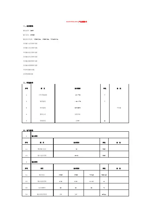
AA251M24-2OL产品规格书一、总体特性输出功率:290W输入电压:48VDC输出电压/电流:5VDC/20A、-5VDC/20A、75VAC/0.3A具有输入过压保护功能具有输入欠压保护功能具有输出过压保护功能具有输出欠压保护功能具有输出限流保护功能具有输出短路保护功能具有铃流输出功能具有热拔插功能二、环境条件序号项目技术指标单位备注1 工作环境温度-10 ~ +40 ℃2 储存温度-40 ~ +70 ℃3 相对湿度20%~90% 不结露4 散热方式自然冷却5 海拔高度≤3000m三、电气特性1输入特性序号项目技术要求单位备注1.1 额定输入电压48 VDC1.2 输入电压范围40~58 VDC2输出特性序号项目技术要求单位备注2.1 输出电压5VDC -5VDC 75VAC VDC/AC2.2 输出电流范围0-200-20 0-0.3 A2.3 电压调整率±4 ±4 ±2 %2.4 输出纹波及噪音≤50 ≤50 mVp-p2.5 动态响应过冲幅度△V:≤±5%Vo2.6 开关机过冲幅度≤10%Vo2.7 效率≥80%2.8 MTBF ≥100,000小时3保护特性序号项目技术要求单位备注3.1 输出过压保护5V 5.5~6.5VDC 空载下测试量-5V -5.5~-6.53.2 输出过流保护额定电流110~150%3.3 输出短路保护输出短路为锁死电源,去掉短路,电源不能恢复正常;重新起动后可恢复正常。
四、安规特性绝缘强度输入—输出1000Vdc/10mA/1min输入—大地500Vdc/10mA/1min输出—大地500Vdc/10mA/1min绝缘电阻输入—输出≥10MΩ输入—大地≥10MΩ输出—大地≥10MΩ五、机械特性及接插件定义(单位:mm)外形尺寸:254×209×25。
6路一线调光低压降恒流型共阳极并联白光LED 驱动器特性y 驱动6路LED ,每路电流20mAyy y y y y y y y y y y 描述AW9356是一款6路低压降恒流型并联TM 封ALD56 -AW9356QNRXY -生产跟踪码D D D D图 1 AW9356QNR 引脚分布及标记图典型应用图图工作温度范围封装形式QFN3x3-16LAW9356R: Tape & Reel绝对最大额定值(注1)电源电压VIN -0.3V to 6 VEN引脚电压-0.3V to VINW (PDmax,package@ TA=25 1.3封装热阻 52℃/W最大结温 125测试标准:JEDEC STANDARD NO.78A FEBURARY 2006 +IT:450mA -IT:-450mA电气特性测试条件:T A=25℃,VIN=3.6V,EN=1(除非特别说明)。
参数条件最小典型最大单位电源电压和电流VIN 输入电源电压 2.85.5VI SD关机电流 EN=0 0.11μAI Q静态电流VIN=3.6V,EN=1,D1~D6引脚悬空1.80 mAT ON启动时间20μs电流源I LED LED电流精度 100%电流,D1至D6 182022mAV drop输出Dropout压降I LED=20mA,V DX-GND 50 mV 任意两路电流匹配度 1%使能引脚ENV IH逻辑高电平 1.3 V V IL逻辑低电平0.3V R EN内置下拉电阻100KΩT LO使能脉冲为低的时间0.5500μsT HI_MIN使能脉冲为高的最短时间0.5 μsT SHDN关机延时当EN由1变为0,AW9356从正常工作到彻底关机的延时800 μs注1:如果器件工作条件超过上述各项极限值,可能对器件造成永久性损坏。
上述参数仅仅是工作条件的极限值,不建议器件工作在推荐条件以外的情况。
器件长时间工作在极限工作条件下,其可靠性及寿命可能受到影响。
产品特色大幅简化离线式LED驱动器设计●单级功率因数校正(PFC)与精确恒流(CC)输出相结合●输入/输出电容和变压器体积小●一次侧反馈控制,无需光耦电路,简化了电路设计●简化初级侧PWM调光接口●符合IEC61000-3-2标准高效节能和高兼容性●大幅提升效率,可达到85%以上●减少元件数量●总谐波失真<15%且PF>0.95●前沿、后沿和数字调光器●传感器和定时器精确稳定的性能●LED负载恒流精度不低于±5%●支持LED负载热插拔●1%-100%宽范围调光,调光无闪烁先进的保护及安全特性●通过自动重启动提供短路保护●开路故障检测模式●自动热关断重启动无论在PCB板上还是在封装上,都保证高压漏极引脚与其他所有信号引脚之间满足高压爬电要求应用●LED离线固态照明说明G7617 是一款的适用于LED调光控制的离线式两级交流/直流电源控制器,是适用于25W 输出功率的可调光LED 灯具的最优之选。
G7617符合电磁兼容性(EMC) IEC61000-3-2 标准,在120V AC或230V AC输入电压下其功率因数(PF) 可达到0.95 以上。
采用先进的数控技术来检测调光器的类型和相位,为调光器提供动态阻抗的同时可调节LED发光亮度,自动检测调光器类型和相位,从而实现了业内与模拟及数字调光器最广泛的兼容性。
G7617工作于准谐振工作模式,工作效率高,可工作于前沿后沿调光模式,也可工作于R 型、R-C型或R-L型调光控制模式。
G7617 符合热插拔LED 模块的固态照明行业标准Zhaga,同时还集成了调光功能的映射选项(位于白炽灯替代灯的NEMA SSL6 调光曲线内)。
G7617 系列有两个版本:针对120V AC输入应用进行优化的G7617-00 和针对230V AC 应用进行优化的G7617-01。
订购信息应用框图图1典型应用内部框图Vcc VinVcbVT CFGASU BisenseBdrvFdrvFisensePGNDAGND C O R E图2 内部框图引脚功能描述BV SENSE V IN BI SENSE B DRV CFG ASU V CCV CBV TFV SENSEFI SENSEF DRVAGNDPGND 图3. 引脚布局BV SENSE引脚:PFC电感电压反馈点,用于感知Boost电感的磁通状态。
180KHz 60V 5A 开关电流升压型LED恒流驱动器XL6006特点⏹5V到32V宽输入电压范围⏹输出电压最高可升压至60V⏹0.22V输出电流采样电压⏹输入电压24V,输出可驱动16串1W/3WLED灯⏹固定180KHz开关频率⏹最大5A开关电流⏹94%以上转换效率⏹出色的线性与负载调整率⏹EN脚TTL关机功能⏹内置功率MOS⏹内置软启动功能⏹内置频率补偿功能⏹内置热关断功能⏹内置限流功能⏹TO263-5L封装应用⏹通用LED照明⏹升压恒流驱动⏹显示器LED背光描述XL6006是一款升压恒流型LED驱动器,具有出色的线性调整率与负载调整率,可以驱动1W/3W/5W的LED灯。
XL6006内置固定频率振荡器与频率补偿电路,简化了电路设计。
当输入电压等于24V时,XL6006可驱动16串1W/3W LED。
PWM控制环路可以调节占空比从0~90%之间线性变化。
内置使能功能、过电流保护功能。
内部补偿模块可以减少外围元器件数量。
图1.XL6006封装180KHz 60V 5A 开关电流升压型LED 恒流驱动器 XL6006引脚配置FB SW EN GNDVIN 12345TO263-5L图2. XL6006引脚配置表1.引脚说明引脚号 引脚名称 描述1 GND 接地引脚。
2 EN 使能引脚,低电平关机,高电平工作,悬空时为高电平。
3 SW 功率开关输出引脚,SW 是输出功率的开关节点。
4 VIN 电源输入引脚,支持DC5V~32V 宽范围电压操作,需要在VIN 与GND 之间并联电解电容以消除噪声。
5 FB反馈引脚,参考电压为0.22V 。
180KHz 60V 5A 开关电流升压型LED 恒流驱动器 XL6006方框图NDMOSVINSWGNDFB2.5V 0.22VCOMP2.5V Regulator 0.22V ReferencePhase CompensationRS LatchUVLOSoft StartThermal ShutdownEAEA ∑Driver OCPOVPENOscillator180KHzSlop Compensation图3. XL6006方框图典型应用XL6006CIN 47uF 35VL1 47uh/5AVIN41253GNDVINSWFBENONOFFI LED =0.22/RSD1 SS38RS 350mASeries 16 1W LEDC1 105COUT 100uF 63VC2 105图4. XL6006典型应用电路180KHz 60V 5A开关电流升压型LED恒流驱动器XL6006订购信息产品型号打印名称封装方式环保认证包装类型XL6006E1 XL6006E1 TO263-5L RoHS & HF 800只每卷绝对最大额定值(注1)参数符号值单位输入电压Vin -0.3到36 V-0.3到Vin V 反馈引脚电压VFB使能引脚电压V-0.3到Vin VEN-0.3到60 V 输出开关引脚电压VSW内部限制mW 功耗PD热阻(TO263-5L)R JA30 o C /W (结到环境,无外部散热片)操作结温T-40到125 o CJ-65到150 o C 贮存温度范围TSTG引脚温度(焊接10秒) T260 o CLEADESD (人体模型) 2000 V 作,在绝对最大额定值条件下长时间工作可能会影响芯片的寿命。
DS9363A-03 April 2011Ordering Information(TOP VIEW)WDFN-10L 3x3Note :Richtek products are :` RoHS compliant and compatible with the current require-ments of IPC/JEDEC J-STD-020.` Suitable for use in SnPb or Pb-free soldering processes.Pin ConfigurationsApplicationsz Mobile Phone, DSC, MP3z White LED Backlighting zLCD Display SupplyMarking InformationFor marking information, contact our sales representative directly or through a Richtek distributor located in your area.3 Channels 90mA x1/x2 Charge Pump White LED DriverGeneral DescriptionThe RT9363A is a compact, high efficient and highly integrated charge pump white LED driver. It maintains the highest efficiency by utilizing a x1/x2 fractional charge pump and low dropout current regulators. The RT9363A supports up to 3 white LEDs and regulates a constant current for uniform intensity. The part implements a 4-bit DAC for brightness control. Users can select external R SET or internal R SET by ISET pin. The dimming of white LEDs'current can be achieved by applying a pulse signal to the EN pin. There are totally 16 steps of current could be set by users. The part can support 15mA to 30mA for the 100%current setting. Users also can use the internal R SET for 100% current setting of 20mA just by connecting the ISET pin to V IN . The operating voltage range is from 2.8V to 5.5V. Internal soft start circuitry effectively reduces the in-rush current while both start-up and mode transition. The load is disconnected from V IN while shutdown and the shutdown current is less than 1uA.RT9363A is available in a WDFN -10L 3x3 package.Featuresz Over 80% Average Efficiency Over Battery Life z Support Up to 3 White LEDsz 80mV Typical Current Source Dropout z Support Up to 90mA Output Current z 1% Typical LED Current Accuracy z 0.7% Typical LED Current Matching z Soft Start Functionz Automatic Charge Pump Mode Selection z 1MHz Random Frequency Oscillator z Over Voltage Protection z 16-Step Brightness Control z Low Input Noise and EMI z Low 1uA Shutdown Current z Flexible Current SettingzRoHS Compliant and 100% Lead (Pb)-FreeLED3LED2CPCN EN ISET VOUT GNDVIN LED1P : Pb FreeG : Green (Halogen Free and Pb Free)Typical Application CircuitFigure 1. Internal R SET(MAX) = 20mA, for 3-WLEDs Application CircuitFigure 2. Internal R SET(MAX) = 20mA, for 2-WLEDs Application CircuitFigure 3. External R SET(MAX) = 15 to 30mA, for 3-WLEDs Application CircuitFigure 4. External R SET(MAX)= 15 to 30mA, for 2-WLEDs Application CircuitDS9363A-03 April 2011Timing DiagramFigure 5. Pulse Dimming WaveformENILEDXFunction Block DiagramEN LED1 LED2 LED3VIN VOUTISETGNDDS9363A-03 April 2011Electrical CharacteristicsAbsolute Maximum Ratings (Note 1)z Supply Input Voltage ------------------------------------------------------------------------------------------------------−0.3V to 6V z Output Voltages -----------------------------------------------------------------------------------------------------------−0.3V to 6V zPower Dissipation, P D @ T A = 25°CWDFN 10L 3x3-------------------------------------------------------------------------------------------------------------1.538W zPackage Thermal Resistance (Note 2)WDFN 10L 3x3, θJA -------------------------------------------------------------------------------------------------------60°C/W WDFN 10L 3x3, θJC -------------------------------------------------------------------------------------------------------8.2°C/W z Junction T emperature -----------------------------------------------------------------------------------------------------150°C z Lead Temperature (Soldering, 10 sec.)-------------------------------------------------------------------------------260°Cz Storage T emperature Range --------------------------------------------------------------------------------------------−65°C to 150°C zESD Susceptibility (Note 3)HBM (Human Body Mode)----------------------------------------------------------------------------------------------2kV MM (Machine Mode)------------------------------------------------------------------------------------------------------200VRecommended Operating Conditions (Note 4)z Junction T emperature Range --------------------------------------------------------------------------------------------−40°C to 125°C zAmbient T emperature Range --------------------------------------------------------------------------------------------−40°C to 85°C(V IN = 3.6V, C IN = C OUT = 2.2uF, C FLY = 1uF, V F = 3.5V, I LED1 = I LED2 = I LED3 = 20mA, ESR = 0.03Ω, T A = 25°C, unless otherwisespecified).To be continuedNote 1. Stresses listed as the above"Absolute Maximum Ratings"may cause permanent damage to the device. These are for stress ratings. Functional operation of the device at these or any other conditions beyond those indicated in the operational sections of the specifications is not implied. Exposure to absolute maximum rating conditions for extended periods may remain possibility to affect device reliability.Note 2. θJA is measured in the natural convection at T A = 25°C on the high effective thermal conductivity four layers thermal test board of JEDEC 51-7 thermal measurement standard. The case point of θJC is on the expose pad.Note 3. Devices are ESD sensitive. Handling precaution is recommended.Note 4. The device is not guaranteed to function outside its operating conditions.DS9363A-03 April 2011Typical Operating CharacteristicsEfficiency vs. Input Voltage2.83.23.644.44.85.25.6Input Voltage (V)E f f i c i e n c y (%)LED Current vs. Input Voltage2.83.23.644.44.85.25.6Input Voltage (V)L E D C u r r e n t (m A )x2 Mode LED Current vs. Temperature161718192021222324-40-30-20-100102030405060708090Temperature L E D C u r r e n t (m A )(°C)x1 Mode LED Current vs. Temperature161718192021222324-40-30-20-100102030405060708090Temperature L E D C u r r e n t (m A )(°C)x1 Mode Quiescent Current vs. Temperature0.60.70.80.91.01.11.21.31.41.51.6-40-30-20-100102030405060708090Temperature Q u i e s c e n t C u r r e n t (m A )(°C)x2 Mode Quiescent Current vs. Temperature1.01.52.02.53.03.54.04.55.0-40-30-20-100102030405060708090Temperature Q u i e s c e n t C u r r e n t (m A )(°C)V IN = 3.7V x1 Mode Dimming OperationTime (5ms/Div)EN (2V/Div)I LED(10mA/Div)V IN = 3.7VV IN = 3.3Vx2 Mode Inrush Current ResponseCN (2V/Div)Time (250us/Div)V OUT (1V/Div)EN (5V/Div)I IN(100mA/Div)x1 Mode Inrush Current ResponseCN (2V/Div)Time (250us/Div)V OUT (1V/Div)EN (5V/Div)I IN(100mA/Div)Frequency vs. Temperature20040060080010001200-40-30-20-100102030405060708090Temperature F r e q u e n c y (k H z )(°C)Shutdown Current vs. Temperature0.00.10.20.30.40.50.60.70.80.91.0-40-30-20-100102030405060708090Temperature S h u t d o w n C u r r e n t (u A )(°C)V IN = 3.3Vx2 Mode Ripple VoltageV IN(50mV/Div)Time (2.5us/Div)V OUT (50mV/Div)CN (2V/Div)I LED(20mA/Div)DS9363A-03 April 2011Application informationThe RT9363A uses a fractional switched capacitor charge pump to power up to three white LEDs with a programmable current. The part integrates current sources and automatic mode selection charge pump. It maintains the high efficiency by utilizing an x1/x2 fractional charge pump and current sources. The small equivalent x1 mode open loop resistance and ultra-low dropout voltage of current source extend the operating time of x1 mode and optimize the efficiency in white LED applications. The operating voltage range is from 2.8V to 5.5V. Internal soft start circuitry effectively reduces the in-rush current while both start-up and mode transition. The load is disconnected from V IN while shutdown and the shutdown current is less than 1uA.High Efficiency x1/x2 Charge PumpBefore the discussion of efficiency in RT9363A, two things need to be illustrated. One is the Li-ion battery life time,the other is the forward voltage of white LED. The Li-ion battery energy is not linearly proportion to battery voltage.In the Figure 6, It shows the 80% battery life of Li-ion is arranged from 3.65V to 4.0V. The other voltage range occupies less than 20% battery energy and is insignificant.In the backlight application, the forward voltage of white LEDs most likely falls in 3.2 to 3.5V @I LED = 20mA. The developing concept of RT9363 is based on the backlight application with Li-ion battery. RT9363A is very cost-effective product for white LEDs backlight driving. It extends the 80% battery life by the reduction of open loop resistance at x1 mode and current source drop out voltage. Figure 7is the efficiency diagram of RT9363 and 80% battery life is marked by red rectangle. The RT9363A maximize the x1 mode operating range in the 80% battery life. Therefore,the efficiency is not significant different to that without x1.5 mode charge pump. The peak efficiency of RT9363A is 93% and the average is 84%. Comparing to the LED drivers with x1.5 mode, only 1 to 2% efficiency loss by x2mode. (Assume 5% battery life in charge pump mode and the efficiency difference of x1.5 and x2 modes is 25%, the efficiency loss thus is 5%x25% = 1.25%).ProtectionThe RT9363A includes a soft start circuit to limit the inrush current at power on and mode transition.Soft start circuit holds the input current level long enough for output capacitor C OUT reaching a desired voltage level.When the soft start off, the RT9363A won't sink spike current from V IN . An over voltage protection function protect the output voltage from dangerous high voltage. The OVP turns off charge pump when the voltage difference between V IN and V OUT is over the designed target.LED Current SettingIn Backlighting part, an internal R SET is used to set the initial current (20mA) of white LED and implements a 4-bit DAC for brightness control. Users can easily configure the LED current by a serial pulse. The dimming of white LEDs'current can be achieved by applying a pulse signal to the EN pin. There are totally 16 steps of current could be set by users. An automatic R SET selection is implemented in this part. RT9363A can automatically select the internal or external R SETs by the connection of ISET pin. The LED current can be calculated by the following equation.where V SET = 1.1V (typ.) and R SET is the external resistor connected from ISET pin to GND.SET LED SET V I = 276R ⎛⎞⎜⎟⎝⎠LED Current Setting TablePCB Board Layoutpad should be connected to a strong ground plane for heat sinking and noise prevention.flying capacitor should be short and wide to reduce parasitic resistance and prevent noise radiation.Output capacitor must be placed close to be placed close to the VIN and connectto GND plane.All the traces of LED and VIN running from chip to LEDs should be wide and short to reduce the parasitic connection resistance and shielded, isolated by ground plane. The Anodes of LEDs Figure 8. PCB Layout GuideFigure 7. Efficiency of RT9363A. (I LED = 60mA, V F = 3.5V)LED Efficiency vs. V IN4050607080901002.62.83.03.23.43.63.84.04.24.4V IN (V)E f f i c i e n c y (%)Figure 6. Li-ion Battery Energy Capacity Versus BatteryVoltage.Capacity (mAH)Battery Voltage(V)4.24.03.655065080%Battery LifeTypical OperationAs shown in the typical application circuit, the power of the RT9363A is provided from the external adapter or battery. When EN pin is low, the white LED for backlighting is turned off and draws a very low current from battery supply.When EN pin is high, RT9363A provides a twice mode load switch (x1) and high efficiency (x2) charge pump device intended for white LED backlight applications. T o maximize the power conversion efficiency, an internal sensing circuit monitors the voltage required on each constant sink input and sets the load switch and charge pump modes based on the input battery voltage and the current sink input voltage. RT9363A provides the option to control the 16-steps brightness of white LEDs with a digital pulse signal applied to EN pin and the detailed timing of pulse dimming is shown in Figure 5.Capacitors SelectionTo get the better performance of RT9363A, the selection of peripherally appropriate capacitor and value is very important. These capacitors determine some parameters such as input and output ripple, power efficiency, maximum supply current by charge pump, and start-up time.To reduce the input and output ripple effectively, the low ESR ceramic capacitors are recommended. Generally,to reduce the output ripple, increasing the output capacitance C OUT is necessary. However, this will increase the start-up time of output voltage. For LED driver applications, the input voltage ripple is more important than the output ripple. Input ripple is controlled by input capacitor C IN , increasing the value of input capacitance can further reduce the ripple. Practically, the input voltage ripple depends on the power supply's impedance. T antalum capacitors are not recommended for the RT9363A. If tantalum must capacitors are needed, C IN and C FLY must larger than 10μF and 1μF. Because tantalum capacitors'values are less than normal when using for high frequency applications. So tantalum capacitor values and ceramic capacitor values can't be the same. But C OUT can't use tantalum capacitor, because during the x2 mode charge pump the V OUT is negative voltage.11DS9363A-03 April 2011Information that is provided by Richtek Technology Corporation is believed to be accurate and reliable. Richtek reserves the right to make any change in circuit design,specification or other related things if necessary without notice at any time. No third party intellectual property infringement of the applications should be guaranteed by users when integrating Richtek products into any application. No legal responsibility for any said applications is assumed by Richtek.Richtek Technology CorporationHeadquarter5F, No. 20, Taiyuen Street, Chupei City Hsinchu, Taiwan, R.O.C.Tel: (8863)5526789 Fax: (8863)5526611Richtek Technology CorporationTaipei Office (Marketing)5F, No. 95, Minchiuan Road, Hsintien City Taipei County, Taiwan, R.O.C.Tel: (8862)86672399 Fax: (8862)86672377Email:*********************W-Type 10L DFN 3x3 Package。
SM16206封装信息管脚定义(SSOP24/QSOP24)S D ID DE X TOUT15S D OO EOUT14OUT13OUT12OUT11O U T 9O U T 8G N DO U T 7O U T 6O U T 5OUT3OUT2OUT1OUT0LEQFN24(4*4)OUT4L K内部功能框图SDI LEOEOUT1SDOFig. SM16206内部功能框图管脚说明订购信息输出及输入等效电路◆OE输入端LE输入端VDDVDD◆CLK,SDI输入端SDO输出端VDDVDD◆OUT0~OUT15输出端NCLKSDI OE LE不用关注SDOOUT0OUT1OUT2OUT3OUT15真值表最大极限参数备注:表贴产品焊接最高峰值温度不能超过 260℃,温度曲线依据 J-STD-020 标准、参考工厂实际和锡膏商建议由工厂自行设定。
(VDD= 5.0V, Ta = 25℃)(VDD=3.3V, Ta = 25℃)直流特性测试电路V DSV IH =V DD V IL =GNDV OH V OL动态特性(VDD= 5.0V, Ta = 25℃)(VDD= 3.3V, Ta = 25℃)动态特性测试电路V IH=V DDV IL=GNDC2时序波形图CLK SDI SDOLE OE OUTnt w(clk)50%50%50%50%50%50%50%50%50%t su(D)t h(D)tpLH,tpHLt h(L)t su(L)t w(L)LOW=outputs enablet pLH1,t pHL1t pLH2,t pHL2OE OUTnt w(OE)50%50%50%50%90%90%10%10%t pHL3t pLH3t of t or产品应用SM16206通道间以及芯片间的电流差异极小,此源自于SM16206优异的恒流输出特性:◆片内通道间的最大电流误差小于±2.5%,而芯片间的最大电流误差小于±3.5%。