LN2401_C南麟中文版规格书PWMPFM 控制DCDC 降压恒流驱动器丝印3AMC
- 格式:pdf
- 大小:372.01 KB
- 文档页数:6
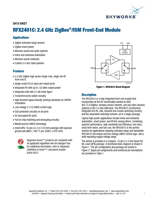
DATA SHEETRFX2401C: 2.4 GHz ZigBee ®/ISM Front-End ModuleApplications∙ ZigBee extended range devices ∙ ZigBee smart power∙ Wireless sound and audio systems ∙ Home and industrial automation ∙ Wireless sensor networks ∙ Custom 2.4 GHz radio systemsFeatures∙ 2.4 GHz ZigBee high-power single-chip, single-die RF front-end IC∙ Single-ended 50 Ω input and output ports ∙ Integrated PA with up to +22 dBm output power ∙ Integrated LNA with 2.5 dB noise figure ∙ Transmit/receive switch circuitry∙ High transmit signal linearity meeting standards for OQPSK modulation∙ Low voltage (1.2 V) CMOS control logic ∙ ESD protection circuitry on all ports ∙ DC decoupled RF ports∙ Full on-chip matching and decoupling circuitry ∙ Market proven CMOS technology∙ Small QFN, 16-pin (3 x 3 x 0.55 mm) package with exposed ground pad (MSL1, 260 ︒C per JEDEC J-STD-020)S kywork s G reen™ product s are compliant with all applicable legi s lation and are halogen-free.For additional information, refer to Skyworks Definition of Green™, document number S Q04-0074.204359-001Figure 1. RFX2401C Block DiagramDescriptionThe RFX2401C is a fully integrated front-end module that incorporates all the RF functionality needed for IEEE802.15.4/ZigBee, wireless sensor network, and any other wireless systems in the 2.4 GHz ISM band. The RFX2401C architecture integrates the PA, LNA, transmit and receive switching circuitry, and the associated matching network, all in a single package. Typical high-power applications include home and industrial automation, smart power, and RF4CE among others. Combining superior performance, high sensitivity and efficiency, low noise, small form factor, and low cost, the RFX2401C is the perfect solution for applications requiring extended range and bandwidth. RFX2401C has simple and low-voltage CMOS control logic, and a wide operating supply voltage range.The device is provided in a compact, 16-pin 3 x 3 mm Quad Flat No-Lead (QFN) package. A functional block diagram is shown in Figure 1. The pin configuration and package are shown inFigure 2. Signal pin assignments and functional pin descriptions are provided in Table 1.204359-002N/C G ND G ND TXRX TXENN/CVDD N/CG ND ANTG NDRXENN/C DN C VDD G ND1651234151413678910111217G NDFigure 2. RFX2401C Pinout(Top View)Table 1. RFX2401C Signal DescriptionsPin Name DescriptionPin Name Description1 N/C Not connected internally 9 GND Ground2GNDGround 10ANTConnect to 50 Ω antenna (DC shorted to GND) 3 GND Ground11 GND Ground4 TXRX RF signal to/from the transceiver (DC shorted to GND) 12 N/C Not connected internally5 TXEN CMOS input to control TX enable 13 DNC Do not connect6 RXEN CMOS input to control RX enable 14 VDD Alternate supply pin, internally connected to pin 167 N/C Not connected internally 15 N/C Not connected internally 8GNDGround16VDDVoltage supply connectionElectrical and Mechanical SpecificationsThe absolute maximum ratings of the RFX2401C are provided in Table 2. The recommended operating conditions are specified in Table 3. The electrical specifications are provided in Tables 4 and 5. The state of the RFX2401C is determined by the logic provided in Table 6.Table 2. RFX2401C Absolute Maximum Ratings1Parameter Conditions Minimum Maximum Units DC VDD voltage supply 0 4.0 VDC control pin voltage Through 1 kΩ resistor 0 3.6 VDC VDD current consumption Through VDD pins when TX is “ON” 350 mADC control pin current consumption 1 μATX RF input power All operating modes +5 dBmANT RF input power When RX is “ON” +5 dBmJunction temperature 150 °CStorage ambient temperature No RF and DC voltages applied -50 +150 o CElectrostatic discharge:Human Body Model (HBM) 3250 V 1Exposure to maximum rating conditions for extended periods may reduce device reliability. There is no damage to device with only one parameter set at the limit and all other parameters set at or below their nominal value. Exceeding any of the limits listed here may result in permanent damage to the device. All maximum RF input power ratings assume 50 Ω terminalimpedance.ESD HANDLING: Although this device is designed to be as robust as possible, electrostatic discharge (ESD) can damage this device.This device must be protected at all times from ESD when handling or transporting. Static charges may easily producepotentials of several kilovolts on the human body or equipment, which can discharge without detection.Industry-standard ESD handling precautions should be used at all times.Table 3. RFX2401C Recommended Operating Conditions1Parameter Conditions Min Typ Max Units DC VDD voltage supply All VDD pins 2.0 3.3 3.6 VControl voltage “high” Through 1 kΩ resistor 1.2 VDD VControl voltage “low” 0 0.3 VOperating ambient temperature Note 2 -40 +125o Cθja35o C/W1 During production test, devices will be tested at 5 V.2 For operation above +85 °C, use the θ ja as guidance for system design to assure the junction temperature will not exceed the maximum of +150 °C.Table 4. RFX2401C Electrical Specifications1 (V DD = 3.3 V, All Unused Ports Terminated with 50 Ω, T A = 25 °C, Unless Otherwise Noted) Parameter Symbol Test Condition Min Typ Max Units Frequency range f 2.4 2.525 GHz Transmit ModeSaturated output power +22 dBm Small-signalgain 21.5 25 26.5 dBSecond harmonic P OUT = +20 dBm, IEEE 802.15.4OQPSK modulation signal–10 dBm/MHzThird harmonic P OUT = +20 dBm, IEEE 802.15.4OQPSK modulation signal–20 dBm/MHzInput return loss –10 dBOutputreturnloss –6 dB Input / output impedance single-ended 50 ΩTX quiescent current No RF applied 17 mATX high-power current P OUT = +20 dBm 90 mALoad VSWR for stability (P OUT = +20 dBm) All non-harmonically related spursless than –43 dBm/MHz6:1 N/ALoad VSWR for ruggedness(P OUT = +20 dBm)No damage 10:1 N/A Receive ModeGain 12 dB Noisefigure 2.5 dB Input return loss –10 dBOutput return loss –12 dBRf port impedance 50 ΩRx quiescent current No RF applied 8 mAInput p1db At ANT pin –8 dBm1 Performance is guaranteed only under the conditions listed in this table.Table 5. RFX2401C Standby Mode Technical ParametersParameter Symbol Test Condition Min Typ Max Units DC shutdown current 1 μATXRX-ANT insertion loss (S21) Pin < -20 dBm –50 dBANT-TXRX insertion loss (S21) –50 dBReturn loss (S11) From TXRX port –1.5 dBTransmit-receive switchingtime 800 nsec Shutdown and “ON” State switchingtime 800 nsecTable 6. RFX2401C Control Logic1Mode TXEN RXENTX active 1 xRX active 0 1Shutdown 00 1 “1” denotes high voltage state (> 1.2 V)“0” denotes low voltage stage (< 0.3 V) at control pins“X” denotes do not care: either “1” or “0” can be appliedApplication Schematic Board DescriptionA suggested RFX2401C FEM application schematic diagram is shown in Figure 3. A schematic of the Evaluation Board is shown in Figure 4.Circuit Design ConsiderationsThe following design considerations are general in nature and must be followed regardless of final use or configuration:∙Paths to ground should be made as short as possible.∙If the transceiver TXRX port has DC present, use a capacitor to block this voltage from reaching the RFX2401C.∙The ground pad of the RFX2401C has special electrical and thermal grounding requirements. This pad is the main thermal conduit for heat dissipation. Because the circuit board acts as the heat sink, it must shunt as much heat as possible from the device.Multiple vias to the grounding layer are e thermal vias to assure efficient heat dissipation. ∙Locate the bypass capacitors as close as possible to the ground pad. Use two ground vias.∙The VDD (pin 14) is an optional VDD pin, internally connected to pin 16.∙The N/C pins 1, 7, 12, and 15 may be left open or connected to GND.∙If the antenna circuits have DC present, use a capacitor to block this voltage from reaching the RFX2401C.NOTE: A poor connection between the ground pad and ground increases junction temperature (T J), which reduces the lifeof the device..J4Figure 3. RFX2401C Application SchematicMA J2SFigure 4. RFX2401C Evaluation Board SchematicPackage DimensionsThe PCB layout footprint for the RFX2401C is shown in Figure 5. Typical part markings are shown in Figure 6. Package dimensions are shown in Figure 7, and tape and reel dimensions are provided in Figure 8.Package and Handling InformationInstructions on the shipping container label regarding exposure to moisture after the container seal is broken must be followed. Otherwise, problems related to moisture absorption may occur when the part is subjected to high temperature during solder assembly.The RFX2401C is rated to Moisture Sensitivity Level 1 (MSL1) at 260 C. It can be used for lead or lead-free soldering. For additional information, refer to the Skyworks Application Note, Solder Reflow Information , document number 200164. Care must be taken when attaching this product, whether it is done manually or in a production solder reflow environment. Production quantities of this product are shipped in a standard tape and reel format.204359-0040.5mm0.25mmFigure 5. RFX2401C PCB Layout Footprint(Top View)204359-006S kywork s Part Number Lot C odeDate C odePin 1Figure 6. Typical Part Markings(Top View)9-007Figure 7. RFX2401C Package DimensionsAll measurements are in millimeters.204359-0083.30 ±0.10Figure 8. RFX2401C Tape and Reel DimensionsDATA SHEET • RFX2401C: 2.4 GHz ZIGBEE/ISM FRONT-END MODULEOrdering InformationModel Name Manufacturing Part Number Evaluation Board Part Number RFX2401C: 2.4 GHz ZigBee/ISM Front-End Module RFX2401C RFX2401C-EK1Copyright © 2016-2017 Skyworks Solutions, Inc. All Rights Reserved.Information in this document is provided in connection with Skyworks Solutions, Inc. (“Skyworks”) products or services. These materials, including the information contained herein, are provided by Skyworks as a service to its customers and may be used for informational purposes only by the customer. Skyworks assumes no responsibility for errors or omissions in these materials or the information contained herein. Skyworks may change its documentation, products, services, specifications or product descriptions at any time, without notice. Skyworks makes no commitment to update the materials or information and shall have no responsibility whatsoever for conflicts, incompatibilities, or other difficulties arising from any future changes.No license, whether express, implied, by estoppel or otherwise, is granted to any intellectual property rights by this document. Skyworks assumes no liability for any materials, products or information provided hereunder, including the sale, distribution, reproduction or use of Skyworks products, information or materials, except as may be provided in Skyworks Terms and Conditions of Sale.THE MATERIALS, PRODUCTS AND INFORMATION ARE PROVIDED “AS IS” WITHOUT WARRANTY OF ANY KIND, WHETHER EXPRESS, IMPLIED, STATUTORY, OR OTHERWISE, INCLUDING FITNESS FOR A PARTICULAR PURPOSE OR USE, MERCHANTABILITY, PERFORMANCE, QUALITY OR NON-INFRINGEMENT OF ANY INTELLECTUAL PROPERTY RIGHT; ALL SUCH WARRANTIES ARE HEREBY EXPRESSLY DISCLAIMED. SKYWORKS DOES NOT WARRANT THE ACCURACY OR COMPLETENESS OF THE INFORMATION, TEXT, GRAPHICS OR OTHER ITEMS CONTAINED WITHIN THESE MATERIALS. SKYWORKS SHALL NOT BE LIABLE FOR ANY DAMAGES, INCLUDING BUT NOT LIMITED TO ANY SPECIAL, INDIRECT, INCIDENTAL, STATUTORY, OR CONSEQUENTIAL DAMAGES, INCLUDING WITHOUT LIMITATION, LOST REVENUES OR LOST PROFITS THAT MAY RESULT FROM THE USE OF THE MATERIALS OR INFORMATION, WHETHER OR NOT THE RECIPIENT OF MATERIALS HAS BEEN ADVISED OF THE POSSIBILITY OF SUCH DAMAGE.Skyworks products are not intended for use in medical, lifesaving or life-sustaining applications, or other equipment in which the failure of the Skyworks products could lead to personal injury, death, physical or environmental damage. Skyworks customers using or selling Skyworks products for use in such applications do so at their own risk and agree to fully indemnify Skyworks for any damages resulting from such improper use or sale.Customers are responsible for their products and applications using Skyworks products, which may deviate from published specifications as a result of design defects, errors, or operation of products outside of published parameters or design specifications. Customers should include design and operating safeguards to minimize these and other risks. Skyworks assumes no liability for applications assistance, customer product design, or damage to any equipment resulting from the use of Skyworks products outside of stated published specifications or parameters.Skyworks and the Skyworks symbol are trademarks or registered trademarks of Skyworks Solutions, Inc., in the United States and other countries. Third-party brands and names are for identification purposes only, and are the property of their respective owners. Additional information, including relevant terms and conditions, posted at , are incorporated by reference.SkyworksSolutions,Inc.•Phone[781]376-3000•Fax[781]376-3100•*********************•204359B • Skyworks Proprietary Information • Products and Product Information are Subject to Change Without Notice • June 16, 2017 11Mouser ElectronicsAuthorized DistributorClick to View Pricing, Inventory, Delivery & Lifecycle Information:S kyworks:RFX2401C RFX2401C-EK1。
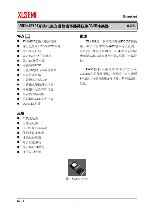
宽输入电压范围n输出电压从1.25V到37V可调n最小压差0.3Vn固定150KHz开关频率n最大3A开关电流n内置功率MOSn出色的线性与负载调整率n内置恒流环路n内置频率补偿功能n内置输出短路保护功能n内置输入过压保护功能n内置热关断功能n推荐输出功率小于13Wn SOP8-EP封装应用n车载充电器n电池充电器n LCD电视与显示屏n便携式设备供电n通讯设备供电n降压恒流驱动n显示器LED背光n通用LED照明描述XL4201是一款高效降压型DC-DC转换器,可工作在DC8V到40V输入电压范围,低纹波,内置功率MOS。
XL4201内置固定频率振荡器与频率补偿电路,简化了电路设计。
PWM控制环路可以调节占空比从0~100%之间线性变化。
内置输出过电流保护功能。
内部补偿模块可以减少外围元器件数量。
图1.XL4201封装150KHz 40V 3A开关电流自带恒流环路降压型DC-DC转换器XL4201引脚配置图2. XL4201引脚配置表1.引脚说明引脚号引脚名称引脚描述1,6 NC 无连接。
2 SW 功率开关输出引脚,SW是输出功率的开关节点。
3 GND 接地引脚。
4 FB 反馈引脚,通过外部电阻分压网络,检测输出电压进行调整,参考电压为1.25V。
5 CS 输出电流检测引脚(IOUT=0.11V/RCS)。
7 VC 内部电压调节旁路电容,需要在VC与VIN之间并联1uF电容。
8 VIN 输入电压,支持DC8V~40V宽范围电压操作,需要在VIN与GND 之间并联电解电容以消除噪声。
背部焊盘为SW150KHz 40V 3A开关电流自带恒流环路降压型DC-DC转换器XL4201 方框图图3. XL4201方框图典型应用(车载充电)图4. XL4201系统参数测量电路150KHz 40V 3A开关电流自带恒流环路降压型DC-DC转换器XL4201典型应用(降压LED恒流驱动)ILED=0.11V/RCS图5.XL4201系统参数测量电路(LED恒流驱动)订购信息产品型号打印名称封装方式包装类型XL4201E1 XL4201E1 SOP8-EP 2500只每卷XLSEMI无铅产品,产品型号带有“E1”后缀的符合RoHS标准。
第1篇一、概述嵌入式控制单元FCU2401是一款高性能、低功耗的嵌入式控制器,适用于工业自动化、智能家居、汽车电子等领域。
本文将详细介绍FCU2401的使用方法,包括硬件连接、软件编程、调试与维护等。
二、硬件连接1. 电源连接将电源线插入FCU2401的电源接口,确保电源电压符合产品规格要求。
FCU2401支持DC12V-24V宽电压输入。
2. 信号输入根据实际需求,将信号线连接到FCU2401的相应输入接口。
FCU2401提供多种信号输入方式,如数字输入、模拟输入、脉冲输入等。
3. 信号输出将信号线连接到FCU2401的相应输出接口。
FCU2401提供多种信号输出方式,如数字输出、模拟输出、PWM输出等。
4. 通信接口根据实际需求,将通信接口线连接到FCU2401的相应接口。
FCU2401支持串口、以太网、CAN等多种通信方式。
三、软件编程1. 开发环境FCU2401支持多种开发环境,如Keil、IAR、MDK等。
以下以Keil为例进行说明。
(1)安装Keil软件:从官方网站下载Keil软件,并按照提示进行安装。
(2)安装MCU驱动程序:从官方网站下载对应的MCU驱动程序,并按照提示进行安装。
(3)创建工程:打开Keil软件,创建一个新工程,选择合适的MCU型号。
2. 编写程序(1)主函数:编写主函数,初始化硬件设备,配置中断、定时器等。
(2)中断服务程序:编写中断服务程序,处理中断事件。
(3)任务函数:编写任务函数,实现具体功能。
3. 编译与下载(1)编译:使用Keil软件编译程序,生成HEX文件。
(2)下载:使用编程器将HEX文件下载到FCU2401。
四、调试与维护1. 调试(1)使用调试器连接FCU2401,设置调试参数。
(2)启动调试器,观察程序运行情况,检查逻辑错误。
(3)修改程序,重新编译、下载,重复调试过程。
2. 维护(1)定期检查硬件设备,确保连接正常。
(2)定期更新程序,修复已知问题。
低压差线性稳压器AAAAAA电源管理单元白光LED驱动DC/DC恒流模式AAAAAA电压检测AAAAAAXT2051 4.25-6.5 1000 40 Linear Y ESOP-8 详情LN2054 4.25-6.5 500 25 Linear Y SOT-23-5,SOT-89-5 详情LN2053 4.25-6.5 1000 25 Linear Y ESOP-8 详情模拟开关产品名称通道工作电压(V) -3dB带宽(MHz) 导通内阻(mΩ)最大电流(mA) 封装形式操作XT9701 1 2.2-6.0 ---- 150 1100 SOT-23-5L 详情LN9703 1 2.0-5.5 ----- 70 3500 SOT-23-5,SOP-8 详情LN9701 1 2.2-6.0 ----- 100 1100 SOT-23-5 详情LN3699 4 1.8-4.2 70 500 200 QFNWB3*3-16 详情LN3005 2 1.8-5.5 30 500 300 MSOP-10 详情霍尔开关产品名称工作电压(V)平均电流(uA)极性及输出方式磁场特性封装形式操作LN4915 1.65-6.0 3 无极性触发,NMOS开漏输出Bops=1.5mT,Bopn=1.5mT,Brps=1.1mT,Brpn=1.1mT,Bhys=0.4mTSOT-23-3,TSOT-23-3,TO-92,TO-92S详情LN4913 1.65-6.0 3 无极性触发,NMOS开漏输出Bops=3.5mT,Bopn=3.5mT,Brps=2.7mT,Brpn=2.6mT,Bhys=0.8mTSOT-23-3,TSOT-23-3,TO-92S详情LN4912 2.4-5.5 4 无极性触发,CMOS输出Bops=3.0mT,Bopn=3.0mT,Brps=2.0mT,Brpn=2.0mT,Bhys=1.0mTSOT-553,SOT-23-3L详情南麟正规授权代理证书沁园春·雪AAAAAA北国风光,千里冰封,万里雪飘。
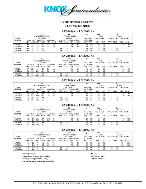
P.O. BOX 609 • ROCKPORT, MAINE 04856 • 207-236-6076 • FAX 207-236-9558 VHF HYPERABRUPTTUNING DIODESLV2001(A) - LV2002(A)C T TR Q V BR I RCAPACITANCE (pF) TUNING RATIO (Vdc) (nAdc) PART f = 1 MHz f = 1 MHz V R = 4 Vdc Ir = 10 µAdc VR = 10 Vdc VR = 20 Vdc NUMBER V R = 4 Vdc V R = 8 Vdc V R =20 Vdc C•4/ C•8V C•4V / C•20V f = 50 MHzMIN MAX MIN MAX MIN MAX MIN MAX MIN MAX MIN / TYP MIN TYP TYP MAX TYP MAX LV2001 18 22 7.5 10.5 3.1 3.9 5.4 6.6 160 220 22 30 15 100 LV2001A 19 21 7.8 9.2 3.1 3.9 5.4 6.6 160 220 22 30 15 100 LV2002 18 22 7.5 10.5 1.8 2.7 160 220 15 18 15 100LV2002A 19 21 7.8 9.2 2.0 2.7 160 220 15 18 15 100 LV2201(A) - LV2202(A)C T TR Q V BR I RCAPACITANCE (pF) TUNING RATIO (Vdc) (nAdc) PART f = 1 MHz f = 1 MHz V R = 4 Vdc Ir = 10 µAdc VR = 10 Vdc VR = 20 Vdc NUMBER V R = 4 Vdc V R = 8 Vdc V R =20 Vdc C•4/ C•8V C•4V / C•20V f = 50 MHzMIN MAX MIN MAX MIN MAX MIN MAX MIN MAX MIN / TYP MIN TYP TYP MAX TYP MAX LV2201 45 55 18 25 7.3 9.2 5.6 6.9 125 165 22 30 20 100 LV2201A 47.5 52.5 18.4 21.6 7.3 9.2 5.6 6.9 125 165 22 30 20 100 LV2202 45 55 18 25 1.8 2.8 125 165 15 18 20 100LV2202A 47.5 52.5 18.4 21.6 2.2 2.8 125 165 15 18 20 100LV2301(A) - LV2302(A)C T TR Q V BR I RCAPACITANCE (pF) TUNING RATIO (Vdc ) (nAdc) PART f = 1 MHz f = 1 MHz V R = 4 Vdc Ir = 10 µAdc VR = 10 Vdc VR = 20 Vdc NUMBER V R = 4 Vdc V R = 8 Vdc V R =20 Vdc C•4/ C•8V C•4V / C•20V f = 50 MHzMIN MAX MIN MAX MIN MAX MIN MAX MIN MAX MIN / TYP MIN TYP TYP MAX TYP MAX LV2301 100 120 39 55 15 19 5.9 7.3 80 110 22 30 30 100 LV2301A 105 115 41.4 48.6 15 19 5.9 7.3 80 110 22 30 30 100 LV2302 100 120 39 55 1.8 2.8 80 110 15 18 30 100LV2302A 105 115 41.4 48.6 2.15 2.8 80 110 15 18 30 100 LV2401(A) - LV2402(A)C T TR Q V BR I RCAPACITANCE (pF) TUNING RATIO (Vdc ) (nAdc) PART f = 1 MHz f = 1 MHz V R = 4 Vdc Ir = 10 µAdc VR = 10 Vdc VR = 20 Vdc NUMBER V R = 4 Vdc V R = 8 Vdc V R =20 Vdc C•4/ C•8V C•4V / C•20V f = 50 MHzMIN MAX MIN MAX MIN MAX MIN MAX MIN MAX MIN / TYP MIN TYP TYP MAX TYP MAX LV2401 140 170 55 80 22.5 28 5.8 7.1 70 90 22 30 50 500 LV2401A 147 163 59.8 70.2 22.5 28 5.8 7.1 70 90 22 30 50 500 LV2402 140 170 55 80 1.8 2.8 70 90 15 18 50 500LV2402A 147 163 59.8 70.2 2.1 2.7 70 90 15 18 50 500LV2501(A) - LV2502(A)C T TR Q V BR I RCAPACITANCE (pF) TUNING RATIO (Vdc) (nAdc) PART f = 1 MHz f = 1 MHz V R = 4 Vdc Ir = 10 µAdc VR = 10 Vdc VR = 20 Vdc NUMBER V R = 4 Vdc V R = 8 Vdc V R =20 Vdc C•4/ C•8V C•4V / C•20V f = 50 MHzMIN MAX MIN MAX MIN MAX MIN MAX MIN MAX MIN / TYP MIN TYP TYP MAX TYP MAX LV2501 180 220 70 105 29 36 5.8 7.1 60 80 22 30 70 500 LV2501A 190 210 78 92 29 36 5.8 7.1 60 80 22 30 70 500 LV2502 180 220 70 105 1.8 2.8 60 80 15 18 70 500LV2502A 190 210 78 92 2.0 2.7 60 80 15 18 70 500Package Style DO-7 Operating Temperature (Topr) -55° to + 150°CStorage Temperature (Tstg) -65° to +200° COther package styles are available元器件交易网。
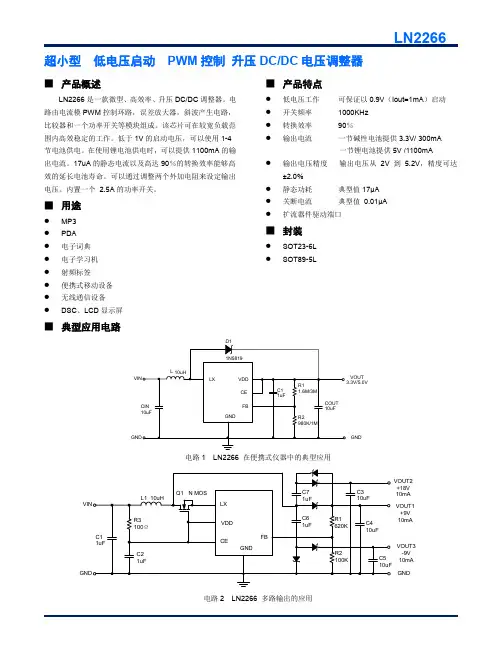
超小型 低电压启动 PWM 控制 升压DC/DC 电压调整器■ 产品概述LN2266是一款微型、高效率、升压DC/DC 调整器。
电路由电流模PWM 控制环路,误差放大器,斜波产生电路,比较器和一个功率开关等模块组成。
该芯片可在较宽负载范围内高效稳定的工作。
低于1V 的启动电压,可以使用1-4节电池供电。
在使用锂电池供电时,可以提供1100mA 的输出电流。
17uA 的静态电流以及高达90%的转换效率能够高效的延长电池寿命。
可以通过调整两个外加电阻来设定输出电压。
内置一个 2.5A 的功率开关。
■ 用途● MP3 ● PDA ● 电子词典 ● 电子学习机 ● 射频标签 ● 便携式移动设备 ● 无线通信设备 ●DSC 、LCD 显示屏■ 产品特点● 低电压工作 可保证以0.9V (Iout=1mA )启动 ● 开关频率 1000KHz ● 转换效率 90%●输出电流 一节碱性电池提供3.3V/ 300mA一节锂电池提供5V /1100mA●输出电压精度 输出电压从2V 到5.2V ,精度可达±2.0%● 静态功耗 典型值17μA ● 关断电流 典型值 0.01μA ● 扩流器件驱动端口■ 封装● SOT23-6L ●SOT89-5L■ 典型应用电路VOUT GND电路1 LN2266 在便携式仪器中的典型应用VOUT1+9V 10mAGNDVOUT2+18V 10mA VOUT3-9V 10mA电路2 LN2266 多路输出的应用■ 订购信息LN2266P ①②③④-⑤■ 引脚配置CE VDD FB SOT89-5L (TOP VIEW)12345CE NC GND FBSOT23-6L (TOP VIEW)LX123465VDDGNDLX■ 引脚分配■ 打印信息SOT23-6L, SOT89-5LSOT89-5L (TOP VIEW)12345SOT23-6L (TOP VIEW)123465① ② ③ ④① ② ③ ④① 表示产品系列② 代表产品的型号③代表基准电压的精度④代表产品生产批号数字0-9,A-Z,倒写数字0-9,A-Z,然后重复(G,I,J,O,Q,W除外)■功能框图VDDFBENGND ■绝对最大额定值■电学特性参数(VIN=1.5V,VDD=3.3V,负载电流=0,T a=25℃,除非另有指定)■特性曲线1.效率——输出电流2.供电电流——输入电压3.开关频率——Vdd端电压4.LX端波形——输出纹波5.瞬态响应6.输出电压——温度7.VIN VS 最大带载 (VOUT=5.0V)■封装信息 SOT23-6LSOT-89-5L。
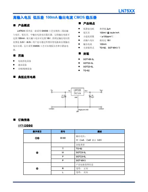
高输入电压低压差100mA输出电流CMOS稳压器■产品概述LN75XX系列是一款采用CMOS工艺实现的三端高输入电压、低压差、中输出电流电压稳压器。
它的输出电流可达到150mA,最大输入电压可达到18V。
其固定输出电压的范围是3.0V~8.0V,用户也可通过外围应用电路来实现输出电压可调。
芯片采用CMOS工艺可实现低压差和小静态电流。
■用途●电池供电设备●通讯设备●音频/视频设备■产品特点●低静态功耗典型值2μA●低压差100mV@Iout=1mA●小温度系数<±100ppm/℃●高输入电压最高达18V●输出电流100mA●小封装形式TO-92,SOT-89-3等■封装●SOT-89-3L●SOT23-3L●SOT23-5L●TO-92■典型应用电路■订购信息LN75①②③④数字项目符号描述①②30-80输出电压:例②=3,③=0表示 3.0V③封装类型T TO-92M SOT23-3LF SOT23-5LP SOT-89-3④产品包装卷带信息R卷带:正向L卷带:反向■打印信息●SOT-89-3、TO-92①②表示产品系列符号产品描述75LN75◆◆◆◆③④表示输出电压值符号产品描述③④输出电压:例③=3,④=0表示 3.0V⑤表示产品批号0~9,A~Z循环(G,I,J,O,Q,W除外)●SOT23-3L、SOT23-5L①表示产品系列符号产品描述5LN75◆◆◆◆②③表示输出电压值符号产品描述②③输出电压:例②=3,③=0表示3.0V④表示产品批号0~9,A~Z循环(G,I,J,O,Q,W除外)■引脚配置■引脚分配引脚号符号引脚说明TO-92SOT23-5L SOT23-3L SOT-89-3L1111GND接地端2232VIN输入端3323VOUT输出端-4,5--NC悬空脚,不接■功能框图■绝对最大额定值项目符号值单位输入电压Vin-0.3~23V功耗SOT-89-3Pd500mW SOT23-3L/SOT23-5L250TO-92300工作温度Topr-40~+85℃贮存温度Tstg-40~+125℃注意:绝对最大额定值是指在任何条件下都不能超过的额定值。
低功耗300mA 低压差CMOS 电压稳压器■ 产品概述LN1132系列是使用CMOS 技术开发的低压差,高精度输出电压,低消耗电流正电压型电压稳压器。
由于内置有低通态电阻晶体管,因而压差低,能够获得较大的输出电流。
为了使负载电流不超过输出晶体管的电流容量,内置了过载电流保护电路、短路保护电路。
此外,因采用SOT23,SOT89等小型封装,故可高密度安装。
■ 用途● 移动电话 ● 无绳电话 ● 相机、摄像机 ● 手持游戏机 ● 手持式AV 设备 ● 基准电压源 ●电池供电设备■ 产品特点●可选择输出电压:可以在1.2~6.0V 的范围内选择,并以0.1 V 为单位进级● 输出电压精度高:精度可达±2.0%●输入输出压差低: 典型值180 mV (输出为3.0V 的产品, I OUT =100mA 时) ● 消耗电流少:典型值5.0μA● 输出电流大:可输出300mA (V IN ≥V OUT +1V ) ● 内置保护:内置过流保护和负载短路保护电路 ● 最大工作电压:7V●采用小型封装:SOT89 ,SOT23以及客户要求的封装■ 封装● SOT89-3L ● SOT89-5L●SOT23-3L ,SOT23-3B ,SOT23-5L■ 典型应用电路VSS VOUTVSS■ 订购信息LN1132 P ①②③④⑤-⑥■ 引脚配置VIN GND CE VOUTSOT23-5L (TOP VIEW)NC12345GND VINVOUT SOT23-3L/B (TOP VIEW)123SOT89-5L (TOP VIEW)12345GND VIN VOUT SOT89-3L (TOP VIEW)123VOUT GND NC VINCE■ 打印信息SOT89-3L,SOT89-5L,SOT23-3L/B,SOT23-5L① ② ③④SOT23-3L/B (TOP VIEW)123① ② ③ ④SOT23-5L (TOP VIEW)12345SOT89-5L (TOP VIEW)12345SOT89-3L (TOP VIEW)123① ② ③ ④① ② ③ ④① 表示产品系列② 代表输出电压范围③ 表示输出电压④ 表示产品批号0~9,A ~Z 循环(G ,I ,J ,O ,Q ,W 除外)■ 功能框图VIN VOUTVSSCE■ 绝对最大额定值注意: 绝对最大额定值是指在任何条件下都不能超过的额定值。
AT2401C产品说明书杭州中科微电子有限公司杭州市滨江区江南大道3850号创新大厦10楼网站:文件编号:AT2401C-20180305版本日期撰写人更新内容1.02017/05/05LYB,QM初稿1.12018/01/05QM更新信息概述AT2401C是一款面向Zigbee,无线传感网络以及其他2.4GHz频段无线系统的全集成射频功能的射频前端单芯片。
AT2401C是采用CMOS工艺实现的单芯片器件,其内部集成了功率放大器(PA),低噪声放大器(LNA),芯片收发开关控制电路,输入输出匹配电路以及谐波滤波电路。
该芯片的常规应用主要包括工业控制自动化,智能家居和符合RF4CE协议的射频系统中。
由于该芯片有非常优越的性能,高灵敏度和效率,低噪声,产品尺寸小以及低成本,使得AT2401C对于频率带宽内的应用而言成为完美的解决方案。
AT2401C的功能控制逻辑电路非常简单,而且使用了少量的外围器件,可以非常方便系统的整体集成设计。
主要应用ZigBee及其相关应用 ZigBee智能电源方案 无线音频系统智能家居和工业自动化 无线传感网络2.4GHz射频系统特性2.4GHz ZigBee高效单芯片射频前端集成芯片集成TX/RX收发器端口和天线端口带谐波抑制的2.4GHz功率放大器低噪声放大器发射/接收开关切换电路满足发射符合OQPSK调制标准的高线性信号的应用要求 低电压CMOS逻辑控制所有端口的ESD保护电路RF端口均有DC隔直电路电源信号VDD与射频信号有良好地内部隔离电路接收通道有低的噪声系数非常低的直流功耗集成全部的匹配以及隔离电路仅需少量的外部器件输入输出匹配到50-Ohm采用性能稳定的CMOS工艺采用QFN3*3*0.55mm的下极板接地的小封装芯片引脚分配芯片引脚分配图绝对最大额定值:参数单位最小值最大值条件电源电压V0 4.0芯片控制引脚电压V0 3.6通过1KOhm的电阻电流mA350当发射控制引脚TXEN为高电平时,通过电源电压的芯片引脚电流芯片控制引脚电流µA1发射信号强度dBm+5所有工作状态天线接收信号强度dBm+5接收控制链路开启芯片存储温度范围℃-50+125没有射频输入以及直流供电的情况下,以及需要根据晶体管结温的要求做一些适当的保护措施备注:超出上述一个或者几个绝对最大额定值可能会导致器件永久性损坏,建议在表中所列范围内使用。
PWM控制的LED驱动器■产品概述LN2115系列是一款固定频率、恒定电流的升压DC/DC 控制器,主要用于手机、PDA和数码相机等设备上的白光背光LED驱动。
输出耐压最高可以达到29 V,输入电压为3.6V 时能同时驱动七路LED每路有3个LED串联,LED的亮度可以外加一个PWM信号来控制。
芯片带过压保护功能。
■用途●LED背光驱动■产品特点●输出耐压:最大可以达到29V●振荡频率: 1.5MHz±20%●效率:88%●工作控制模式:PWM控制的电流模工作模式●待机功耗:最大1.0μA●PWM调光:最小调光5%,调光频率100KHZ ■封装●SOT23-6L■应用电路VOUTVIN注:电路中R LED=V FB/(I LED*n),V FB为FB端输出电压,n为LED并联的路数,I LED为流过每一路LED灯的电流。
CL必须使用10uF以上电容;■订购信息■ 引脚配置LX GND FB VINSOT-23-6L (TOP VIEW)CE123465OVP■ 打印信息SOT-23-6L (TOP VIEW)① ② ③ ④123465① 代表产品名②③ 代表产品FB 端电压范围和类型④ 代表生产批号数字0-9,A-Z ,倒写数字0-9,A-Z ,然后重复(G ,I ,J ,O ,Q ,W 除外)■ 功能框图■绝对最大额定值注意:绝对最大额定值是指在任何条件下都不能超过的额定值。
万一超过此额定值,有可能造成产品劣化等物理性损伤。
■电学特性参数■测试电路L:4.7uHVIN测试电路1测试电路2测试电路3测试电路4 注:所有测试电路中R LED=V FB/I LED,V FB为FB端输出电压,I LED=20mA; 如V FB=0.25V,则R LED=12.5Ω■特性曲线不同频率下PWM调光结果(V IN=3.8V,CIN=1uF,CL=10uF,L=4.7uH)●LED电流设定升压回路提供的电压可以保证FB电压与内部基准电压相等,因此当R LED接到FB与GND上时,V OUT流过LED的电流和R LED流到GND的电流可以由R LED设定,电流计算公式如下:I LED=0.25/R LED●调光控制PWM型号接CE脚调节方式对于亮度,当CE脚接高电平时,芯片内部提供一个典型的0.25V的基准电压,可以使亮度达到最大。
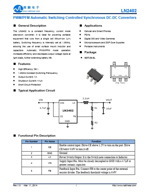
PWM/PFM控制DC-DC降压恒流驱动器
■产品概述
LN2401是一款由基准电压源、振荡电路、比较器、PWM/PFM 控制电路等构成的CMOS降压恒流驱动器。
利用PWM/PFM自动切换控制电路达到可调占空比,具有全输入电压范围(2.0-6V)内的低纹波、高效率和大输出电流等特点。
LN2401内置功率MOSFET,使用过压、过流、过热等诸多保护电路,在超过控制值时会自动断开,以保护芯片。
本产品结合了微型封装和低消耗电流等特点,最适合在移动设备的电源内部使用。
■产品特点
●高效率最大效率可达92%
●大的输出电流800mA
●甚小静态电流200μA
●低压操作可达100%占空比
●PWM/PFM自动切换占空比自动可调以保持很大负
载范围内的高效率、低纹波
■用途
●LED驱动
■封装
●SOT23-5L
■典型应用电路
LED+
LED-
注:I LED=0.1V/R SET
■订购信息
LN2401 ①②③-④
■ 引脚配置
CE GND LX FB
SOT23-5L (TOP VIEW)
VIN
1
2
3
45
■ 打印信息
SOT23-5L
① ② ③ ④
SOT23-5L (TOP VIEW)
1
2
3
4
5
① 表示产品系列
② 表示反馈电压值
③ 表示封装形式
④ 代表生产批号
数字0-9,A-Z ,倒写数字0-9,A-Z ,然后重复(G ,I ,J ,O ,Q ,W 除外)
■绝对最大额定值
■功能框图
■ 电学特性参数
VIN=5V ,C IN =4.7µF ,C OUT =10µF ,L=2.2µH (Ta=25 ℃除非特殊指定)
■ FB 调光
LN2401支持在FB 端调光,如下图所示。
LED+
LED-
使用如下公式计算ILED :
其中VD 为直流电压。
举例说明:
RSET=0.1ohm ,VD=0.15V ,R1=R2=1K ,ILED=500mA 。
除了在VD 端可以直接加模拟电压调光外,也可以通过下图所示的方式,以PWM 信号调光。
LED+
LED-
VH VL
RS 和CS 组成的低通滤波器将数字信号PWM 转换为模拟信号VD 。
VD=(VH-VL)*D ,D 为PWM 信号的占空比,VH 和VL 分别为PWM 信号的高低电平。
举例说明:
PWM 信号频率100K ,选择RS=10K ,CS=0.1uF 。
PWM 信号高电平1.8V ,低电平0V ,占空比10%,则VD=0.18V , 选择R1=R2=1K ,RSET=0.1ohm , 根据如下公式:
计算得到ILED=200mA 。
RS 和CS 的值取决于PWM 调光的频率,频率越低则RS 和CS 的值要选择越大。
■ 封装信息
SOT23-5L。