Ansoft_HFSS进行腔体滤波器设计
- 格式:ppt
- 大小:4.30 MB
- 文档页数:20
基于HFSS的微调谐腔体带通滤波器设计发表时间:2016-10-12T14:41:17.417Z 来源:《电力设备》2016年第14期作者:李婷婷[导读] 针对微调谐腔体带通滤波器设计制造中存在的问题,介绍了腔体带通滤波器的总体设计。
(广州海格通信集团股份有限公司)摘要:针对微调谐腔体带通滤波器设计制造中存在的问题,介绍了腔体带通滤波器的总体设计;论述了需要解决的问题,如优化计算、提高仿真精度和简化调谐结构,并对二端口网络等效替换、整体仿真和微调谐关键技术进行了分析。
关键词:腔体带通滤波器;微调谐;免调谐;HFSS传统的微波腔体带通滤波器的设计过程中,参数计算量大,仿真存在误差,调谐过程耗时费力。
随着腔体带通滤波器在微波通信设备中的广泛应用,其设计方法有待改进。
通过设计参数求取方法的改进和对原理图的完善补充以及采用合理的仿真过程,确保了滤波器设计的精确度。
在此基础上,摒弃传统的用调谐螺钉调谐的方式,采用微调谐结构的腔体来实现滤波器的微调谐,配合线切割加工工艺,最终实现腔体带通滤波器的精确微调谐设计,一定的相对带宽条件下,可实现免调谐设计。
一、总体设计微波腔体带通滤波器的设计过程大体分为3步:一是按设计要求求取设计参数;二是进行滤波器模型的仿真;三是进行滤波器的调谐。
求取设计参数一般先根据设计要求选择合适的切比雪夫低通原型滤波器,因为较之最大平坦型滤波器,切比雪夫滤波器有更优异的带外抑制,较之椭圆函数滤波器更易于实现。
进行模型仿真前,还需要得到以下3个参数:一是单端输入最大群时延;二是谐振器间耦合系数;三是谐振腔的谐振频率。
滤波器模型的仿真分为2步:第一步要在HFSS中建立滤波器的三维微调谐模型;第二步就是进行HFSS的模型仿真。
在HFSS中建立滤波器腔体模型后,对其先后进行单谐振器本征模仿真、双谐振器本征模仿真和单端输入最大群时延仿真,分别得到单谐振器谐振频率、相邻谐振器间耦合系数和单端输入最大群时延等参数的仿真值。
利用HFSS 对腔体滤波器的精确设计黎涛 赵霞上海航天测控通信研究所 200086摘要 本文用一个实例介绍了一种设计思路,借助计算机利用Ansoft 公司的HFSS 软件对腔体交指型滤波器进行精确设计,实验表明用这种方法设计的滤波器有通带平坦、插损小、精确度高等特点。
一. 引言在微波带通滤波器的设计中,我们经常采用腔体交指型结构。
它具有插损小、带外抑制度高、结构紧凑、体积小等优点。
对于腔体交指型带通滤波器的设计,现在比较广泛的的思路是:只考虑相邻两耦合杆之间的耦合关系,忽略相邻杆以外的边缘电容的影响,因而采用两个沿结构传输的TEM 正交模来描述,即奇模和偶模。
而实际在这种滤波器结构中所有的谐振杆之间都存在耦合,因此这种方法只是一种简化的近似设计。
采用这种方法设计的产品性能差,表现在带内插损和波纹大,矩形系数不好等,一般无法满足现在通讯的要求,我们还要花大量的精力对滤波器进行调整,以提高其性能。
甚至需要重新加工再生产,这大大增加了产品的研制成本和周期。
因此我们必须对滤波器进行精确的设计,即在工程设计中将所有谐振杆的耦合都考虑进去,而这不是传统的手工计算可以完成的,必须借助计算机软件进行辅助设计。
自上世纪70年代以来,CAD 工具在微波工程领域得到越来越广泛的应用。
经过多年的发展,目前国内外已有多种微波CAD 软件,而以Ansoft 公司的HFSS 效果最佳。
通过该软件我们可以方便的得到各种物理模型,进而对该模型进行电磁场的仿真。
计算结束后我们就可以得到所需的场结构和相关的S 参数,也就知道了该滤波器的电性能情况。
二. 设计下面通过一个S 波段的五级滤波器的设计实例加以说明。
首先我们通过简化的近似计算得到该滤波器的几何数据的初值,由于这类滤波器的粗略设计的方法已经很成熟,因此这里不进行详细介绍,直接给出(详细情况可参看《现代微波滤波器的结构与设计》)。
但这一步也是非常重要的,初值的好坏直接关系到我们利用软件计算优化的快慢。

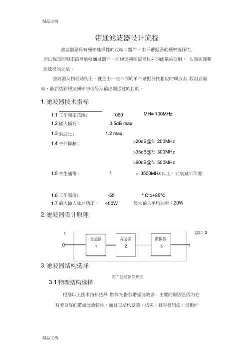
带通滤波器设计流程滤波器是具有频率选择性的双端口器件。
由于谐振器的频率选择性,所以规定的频率信号能够通过器件,而规定频率信号以外的能量被反射, 从而实现频率选择的功能。
滤波器从物理结构上,就是由一些不同的单个谐振器按相应的耦合系 数组合而成,最后达到规定频率的信号从输出端通过的目的。
1. 滤波器技术指标1.1 工作频率范围: 1060MH ± 100MHz1.2插入损耗: 0.5dB max1.3 驻波比:1.2 max1.4 带外抑制:>20dB@f ± 200MHz >35dB@f ± 300MHz >60dB@f ± 500MHz1.5 寄生通带: f > 3500MHz 以上,对衰减不作要1.6 工作温度:-55 ° Cto+85°C1.7 最大输入脉冲功率:400W最大输入平均功率:20W2. 滤波器设计原理3. 滤波器结构选择3.1物理结构选择根据以上技术指标选择 腔体交指型带通滤波器,主要的原因是因为它 有着良好的带通滤波特性,而且它结构紧凑、结实;且容易制造;谐振杆端口 2图1滤波器原理图的长度近似约为入/ 4(波长)°,故第二通带在3倍fo上,其间不会有寄生响应。
它用较粗谐振杆作自行支撑而不用介质,谐振杆做成圆杆,还可用集总电容加载的方法来减小体积和增加电场强度,而且它适用于各种带宽和各种精度的设计。
3.2电路结构的选择根据以上技术指标选择交指点接触形式,主要的原因是它的谐振杆的一端是开路,一端是短路(即和接地板接连在一起),长约入/ 4 °,载TE M (电磁波)模,杆1到杆n都用作谐振器,同时杆1和杆n也起着阻抗变换作用。
4. 电路仿真设计如图2模型选择。
采用An soft公司的Serenade设计,根据具体的技术指标、体积要求和功率容量的考虑,此滤波器采用腔体交指滤波器类型,使用切比雪夫原型来设计,用圆杆结构的物理方式来实现。
本科生毕业论文设计题目: 3.4GHz 梳状线腔体滤波器的设计系 部 学科门类 工 学 专 业 电子信息工程 学 号姓 名指导教师年 月 日装 订 线3.4GHz梳状线腔体滤波器的设计摘要在当今通信领域中,微波滤波器在通信设备中占有重要的地位,在微波毫米波通信、卫星通信、雷达、导航、制导、电子对抗、测试仪表等系统中,有着广泛的应用。
梳状线滤波器具有小体积、高Q值、高功率容量等优点,是微波滤波器中常见的腔体形式,工程实用性较强,广泛应用于通信及其它领域。
本文从滤波器的工作原理出发,分析了梳状线带通滤波器的结构特征,并利用软件Ansoft HFSS进行仿真,最后基于仿真结果制作出实物并进行了调试,使其最终达到预期的指标。
关键词:梳状线滤波器仿真调试ABSTRACTIn the field of current communication, Comb-line filters occupies an important position in communication equipment. Microwave filters has a wide range of applications in microwave communication, millimeter wave communication, satellite communication, radar, navigation, guidance, electronic against, testing instruments system. Comb-line filters have small size, high Q value, high power capacity etc, and is common in microwave filters of the recessed forms, therefore it widely used in communications and other fields . Based on the theory of filters, the structure characters of comb-line band-pass filter have been analyzed and the typical parameters have been calculated. Then the filter is simulated with software Ansoft HFSS. At last, I have manufactured a practicality based on the results of simulation and debugged it for the purpose of achieving anticipative targets.Key words:Comb-line Filter Simulation Debug目录一绪论 (1)1.1 课题来源与意义 (1)1.2 国内外发展状况 (1)1.3 课题的研究内容、方法及手段 (1)二梳状线滤波器的综合介绍 (3)2.1 梳状线滤波器的特点 (3)2.2 梳状线滤波器的结构 (3)2.3 梳状线滤波器的工作原理 (3)三梳状线滤波器的设计 (4)3.1 梳状线滤波器设计思路 (4)3.2 梳状线滤波器的技术指标 (4)3.3 梳状线滤波器的归一化原型 (4)3.4 频率变换 (5)3.5 相关的理论计算过程 (5)四运用Ansoft HFSS进行仿真设计 (7)4.1 单腔模型及仿真结果 (7)4.2 双腔模型及仿真结果 (8)五梳状线滤波器的实物制作与测试 (11)六总结与结论 (12)参考文献 (13)一绪论1.1 课题来源与意义本课题来源于科研生产。
hfss腔体滤波器设计实例HFSS(High Frequency Structure Simulator)是一种用于电磁场仿真和分析的软件工具。
它广泛应用于高频电磁场的建模和分析,可用于设计各种射频(RF)和微波器件,如天线、滤波器、耦合器等。
本文将以HFSS腔体滤波器设计实例为题,介绍如何利用HFSS软件进行腔体滤波器的设计。
我们需要明确腔体滤波器的基本原理。
腔体滤波器利用腔体的谐振模式和谐振频率来实现信号的滤波。
通过调整腔体的几何参数和材料特性,可以实现对特定频率范围内的信号进行滤波。
因此,腔体滤波器的设计关键在于确定合适的腔体结构和参数。
接下来,我们将以一个实际的设计例子来具体介绍HFSS腔体滤波器的设计流程。
假设我们要设计一个工作在2.4GHz频段的微波腔体滤波器。
首先,我们需要选择合适的腔体结构。
常见的腔体结构有矩形腔体、圆柱腔体等,根据设计要求选择合适的结构。
在HFSS中,我们可以通过绘制几何模型来定义腔体结构。
绘制完成后,我们需要定义腔体的材料属性,包括介电常数、磁导率等。
这些参数将直接影响腔体的谐振频率和模式。
接下来,我们可以利用HFSS的求解器进行电磁场仿真。
在仿真前,我们需要设置仿真的频率范围和精度。
根据设计要求,选择合适的频率范围,并设置适当的网格精度。
仿真完成后,我们可以通过HFSS的结果分析工具来分析仿真结果。
主要包括频率响应、S参数、电场分布等。
根据设计要求,对仿真结果进行评估和调整。
如果需要改善滤波器性能,可以通过调整腔体的几何参数和材料特性来实现。
在设计过程中,需要注意以下几点。
首先,腔体的尺寸和几何参数应该合理选择,以满足设计要求。
其次,材料的选择和特性对滤波器性能影响很大,需要选择合适的材料并设置正确的特性。
最后,仿真结果的准确性和稳定性也需要重视,可以通过调整网格精度和求解器参数来提高仿真结果的准确性。
HFSS是一种强大的工具,可以用于腔体滤波器的设计和分析。
第30卷 第2期2007年4月电子器件Chinese J ournal Of Elect ron DevicesVol.30 No.2Ap r.2007Design of Coaxial Filters B ased On HFSSL I U Pen g 2y u1,2,Z H A N G Yu 2hu 2,S H EN H ai 2gen11.School of Elect ronic I nf ormation and Elect ric Engineering ,S hanghai J iao Tong Universit y ,S hanghai 200240,China;2.S hanghai S pacef li ght I nstit ute of T T &C and Telecommuniation ,S hanghai 200086,Chi naAbstract :Coaxial filters is widly used in microwave circuit s.we research how to analysis and design coaxial filters used by a 3D f ull 2wave field solver ,HFSS.The 3D f ull -wave field analysis includes t he effect s of t uning screw ,interstage coupling apert ure and inp ut/outp ut coaxial excitation.Base on t hess analysises ,we work out a S -band coaxial filter aided by simulating and optimizing in HFSS.The result of t he experi 2mentation matched well wit h t he result of simulation ,and f ulfiled technic target s.The coaxial filter has been used in a spaceflight project successf ully.The way of combining t he t raditional t heory wit h t he ad 2vanced comp uter technology has great practical value ,it can save much time and co st .K ey w ords :microwave filters ;coaxial resonator ;coupling apert ure ;HFSS EEACC :1320基于HFSS 设计同轴腔滤波器刘鹏宇1,2,张玉虎2,沈海根1(1.上海交通大学电子信息与电气工程学院,上海200240;2.上海航天测控通信研究所,上海200086)收稿日期:2006204217作者简介:刘鹏宇(19782),男,工作于上海航天测控通信研究所,工程师,主要研究方向为射频与微波电路设计,pengyu_liu @ ;摘 要:同轴腔滤波器在微波电路中有着广泛的应用,在此研究如何利用3D 全波场分析软件HFSS 分析设计同轴腔滤波器.该分析包括谐振腔调谐螺钉、腔间耦合孔及输入输出激励的影响效应.基于上述分析,借助HFSS 仿真优化得到一S 波段滤波器.其实测结果与仿真相符,满足指标要求,并已成功应用于某航天工程中.这种结合传统理论和先进计算机技术的方法可以大大节省研制周期和生产成本,具有非常大的实用价值.关键词:微波滤波器;同轴谐振腔;耦合孔;HFSS 中图分类号:TN 713 文献标识码:A 文章编号:100529490(2007)022******* 传统的微波滤波器设计方法已经非常成熟,但其中一些参数需要反复试验来获得.这势必要增加产品的设计周期,对于当前研制周期紧、产品数量大的要求是一个制约.利用仿真工具进行辅助设计成为目前一种非常有效的解决途径.本文即介绍如何借助H FSS 设计同轴腔滤波器.1 HFSS 简介HFSS 是ANSO F T 公司开发的一个基于物理原型的EDA 设计软件.使用H FSS 建立结构模型进行3D 全波场分析,可以计算.①基本电磁场数值解和开边界问题,近远场辐射问题;②端口特征阻抗和传输常数;③S 参数和相应端口阻抗的归一化S 参数;④结构的本征模或谐振解.依靠其对电磁场精确分析的性能,使用户能够方便快速地建立产品虚拟样机,以便在物理样机制造之前,准确有效地把握产品特性,被广泛应用于射频和微波器件、天线和馈源、高速IC 芯片等产品设计中.H FSS 有本征模解(Eigenmode Solution )和激励解(Driven Solution )两种求解方式.选择Eigen 2mode Solution 用于计算某一结构的谐振频率以及谐振频率点的场值和腔的空载Q0值.选择Driven Solution用于计算无源高频结构的S参数和特性端口阻抗、传播常数等.本课题的研究中,将用到本征模解求解单同轴腔特性和腔间耦合系数;激励解求解有载品质因数Q L值和滤波器响应特性.2 同轴腔滤波器工作原理及设计2.1 工作原理同轴腔滤波器主要用于米波、分米波段.传输TEM模,无色散、场结构简单稳定、空载品质因数高[1].其基本结构由谐振腔、腔间耦合、输入输出激励组成,如图1所示即为一个三腔同轴滤波器.输入信号通过闭合圆环耦合到谐振腔中产生谐振,能量在谐振腔之间由耦合孔进行逐级耦合,再经图1 三腔同轴滤波器结构模型(a=3.25mm,b=9mm,l=29mm,l1=l2=14mm)过输出端的闭合圆环耦合输出.各腔均工作在同一谐振频率附近,只有该谐振频率附近的电磁波有效传输,形成一带通滤波器.2.2 集总参数网络设计下面以S波段滤波器设计为例,主要技术指标见表1.表1 滤波器技术指标技术参数工作频率f0插入损耗L A带宽(4f3dB)通带波动L Ar阻带抑制L As(f0±15M Hz)输入输出阻抗Z o指标要求2.0~2.15GHz≤2dB≥8M Hz≤±0.3dB≥25dB50Ω 利用网络综合法[2],选取切比雪夫函数作为逼近函数,查表或计算[3]确定滤波器阶数n=3,对应的低通原型参数:g0=g4=1,g1=g3=1.0316,g2=1.1474,由此得到腔间耦合系数K ij和外部品质因数Q L.K ij=bwg i・g j=0.0036(i=1,j=2;i=2,j=3)(1)Q L=g1bw=266.3(2)2.3 微波结构设计2.3.1 同轴腔为减小体积和便于安装,本滤波器采用内圆外方的1/4λ缩短电容同轴腔结构.依据谐振腔结构尺寸参数选取三个原则[1]:①避免高次模,(a+b)≤λmin/π;②满足功率容量,b/a=1.65时功率容量最大;③损耗要小,b/a=3.6时Q0值最高,损耗最小.b/a一般选择在2.0~3.6之间.在此选取内导体半径a=3.25mm,外导体内半径b=9mm.内导体长度l、调谐螺钉最大调谐距离t的设计既要考虑能够满足所需的调谐范围,同时还要考虑到内导体缩短会降低Q0值[4]的因素,一般选择内导体长度为1/4λ的65%以上,在此选取l=29mm,t=3mm.谐振腔的调谐范围将通过HFSS进行仿真验算.2.3.2 耦合考虑到本滤波器属于窄带滤波器,腔间耦合[5]采用圆孔实现,输入输出耦合采用闭合半圆环实现.耦合圆孔、半圆环需要确定的参数是中心位置和半径大小.滤波器带宽基本上由级间耦合决定.设计一个在某个频率范围内可调谐的滤波器时,若要保持固定的带宽,则必须控制带宽对频率的敏感性,即要保持d(Δf)/d f=0.Cohn[6]研究得出,当耦合孔中心离腔短路端距离l1在中心频率电长度36°附近时,耦合带宽最大且随频率变化缓慢.则取l1=14mm.半圆环的几何位置通常与耦合孔保持一致,所以也取l2=14mm.关于耦合孔径的大小,下面通过HFSS仿真腔间耦合系数K ij和外部品质因数Q L获取.3 HFSS仿真分析3.1 单谐振腔仿真根据选定的结构尺寸(a=3.25mm,b=9mm, l=29mm),在H FSS中对单谐振腔建模(图2),不需要加载激励,进行Eigenmode分析,获取在不同间距t的加载电容下对应的谐振频率.仿真结果(图3)得出,当t在0.25~3mm之间调整,对应谐振频率范围在1619~2171M Hz之间变化,可以满足要求.图2 单谐振腔模型 图3 谐振频率与加载电容关系3.2 腔间耦合系数K ij仿真腔间耦合的电性能用耦合系数K ij表示.当两134第2期刘鹏宇,张玉虎等:基于H FSS设计同轴腔滤波器个相邻的谐振腔耦合在一起、并且对源和负载具有非常小的耦合时,K ij 与相邻腔谐振频率f 1、f 2存在如下关系[7]:K 12=2(f 2-f 1)/(f 2+f 1)(3)因此,对两个相邻谐振腔在不接源和负载(图4)情况下进行Eigenmode 分析(modes =2),得到在不同圆孔半径下对应的谐振频率f 1、f 2,从而绘制出对应的腔间耦合系数曲线(图5).结果表明耦合孔越大,耦合越强.图4 腔间耦合系数仿真模型图5 耦合圆孔与耦合系数关系3.3 有载品质因数Q L 仿真当单个谐振腔耦合源和负载时,有载品质因数Q L 与谐振频率f o 及3dB 带宽Δf 3dB 存在如下关系[7]:Q L =f o /Δf 3dB(4)建立模型对单谐振腔加载源和负载(图6),进图6 有载品质因数 图7 耦合圆环与有载品质仿真模型因数关系行Driven Terminal 分析,得到在不同耦合圆环半径下对应的有载品质因数Q L 曲线(图7).耦合环越大,耦合越强,Q L 值越低. 根据公式(1)、(2)中计算结果,对照以上仿真分析图表,即可选取适当的结构参数,在H FSS 中完成整个滤波器的建模(图1),经过进一步优化,获取理想的特性曲线,确定最终的结构尺寸:r _apert ure =3.18mm ,r _loop =2.6mm .4 实测结果与分析综合上述设计及优化结果,并考虑到为实物调试时留有一定的调整余量,耦合孔和耦合环半径均取的略小一些,确定最终的加工尺寸见表2.表2 同轴腔滤波器结构加工尺寸结构参数a bltl 1l 2r _loop r _aperture尺寸/mm 3.25929314142.53 按照表2结构尺寸机械加工,进行适当的谐振频率和耦合调整,获得了满意的特性曲线(图8),达到技术指标要求(表3).结果表明,插入损耗、带外抑制实测结果比与仿真结果要差一些.这是可以理解的,因为HFSS 仿真是在理想边界条件下进行的,而滤波器实物是由三个单谐振腔和输入输出端口组合在一起的,,还有腔体内部镀银表面不光滑,这些都会引入损耗[8],导致Q 0值降低,使得插损、带外抑制指标略有变差.图8 实测(粗线)与仿真(细线)滤波器响应表3 滤波器测试数据技术参数工作频率f 0插入损耗L A带宽(Δf 3dB )通带波动L Ar 阻带抑制L A s(f 0±15M Hz )驻波比指标要求2.065GHz 1.75dB8.5M Hz 0.15dB33.6dB1.345 结束语本文利用ANSO F T HFSS 仿真软件对同轴腔滤波器中的谐振腔、腔间耦合及输入输出激励进行了优化设计,确定了滤波器实际结构尺寸,测试结果与仿真一致.该方法可以有效并准确地替代传统试验方法,也可以应用在其它的微波滤波器设计中.参考文献:[1] 廖承恩,陈达章.微波技术基础[M].北京:国防工业出版社,1979.[2] 甘本,吴万春.现代微波滤波器的结构与设计[M].北京:科学技术出版社,1973.[3] Hong Jia 2Sheng.Microstrip Filters for RF/Microwave Applications ,ncaster C opyrightc 2001John W illy &S ons ,Inc.pp.29261.[4] K urzrok R.M.Design of C omb 2Line Band 2Pass Filters (C orrespon 2dence )[J ].T ransactions on Microwave Theory and T echniques ,Jul.1966,T 2MTT 214(7):3512353.[5] 姚毅,黄尚锐.调谐滤波器的腔间耦合结构研究[J ].微波学报,1994(1):16222.[6] K urzrok R M.Design of Interstate C oupling Apertures for Narrow 2Band T unable C oaxial F ilters[J ].(C orrespondence )IRE T rans.on M i 2crowave ’Theory and T echniques ,March ,1961,MTT 210:1432144.[7] Randall W.Rhea ,HF Filter Design and Computer Simulation[M ].Mc Graw 2Hill ,Inc.,1995.[8] 高葆新.波导带通滤波器的设计[J ].国外电子测量技术,2001(1):34237.234电 子 器 件第30卷。
Efficient Design of Chebychev Band-Pass Filters with Ansoft HFSS and SerenadeTutorialDr. B. Mayer and Dr. M.H. VogelAnsoft CorporationContentsAbstract 31. Introduction 32. Circuit Representation of the Filter 53. Relationships between Circuit Components and Physical Dimensions in the Microwave Filter 104. Initial Filter Design in HFSS 145. Curve Fitting in Serenade 166. Corrected Filter Design in HFSS 207. Additional Information from the 3D Field Solver 21 7a. Effects of Internal Losses 21 7b. Maximum power-handling capability 23 7c. Mechanical Tolerances 24 References 25 Appendix A Derivation of the Circuit 26 Appendix B The Physical Meanings of K and Q 43AbstractAn efficient method is presented to design coaxial Chebychev band-pass filters. The method involves a 3D full-wave field solver, Ansoft HFSS, teaming up with a circuit simulator, Serenade. The authors show how for a practical case, a 7-pole band pass filter with a ripple of only 0.1 dB, an accurate design is obtained in a matter of days, as opposed to weeks for traditional methods.The method described is also applicable to even more challenging designs of elliptic filters and phase equalizers realized in dielectric, waveguide or coaxial technology.1 IntroductionIn this paper, we will describe an efficient method to design a filter. The method involves a 3D full-wave field solver teaming up with a circuit simulator. The basic idea has been explored by others [1] but a different circuit was used in the circuit simulator. We will explain our procedure by presenting in detail how we design a Chebychev band pass filter with the following specifications:Center frequency 400 MHzRipple bandwidth 15 MHzRipple 0.1 dBOut-of-band rejection 24 dB at 390 MHz and at 410 MHzIn order to achieve the out-of-band rejection, we will need seven poles.The desired filter characteristic is shown in Fig. 1.Fig. 1 Desired filter characteristicAs the basic geometry for this filter we have chosen a cavity with seven coaxial resonators, as shown in Fig. 2. In the figure, the “buckets” have been drawn as wire frames for clarity, to show that the cylinders don‟t extend all the wa y to the bottom.Fig. 2 Basic filter geometryThis geometry is symmetrical with respect to the central cylinder. In this kind of filter, the walls of the cavity, the long cylinders, the buckets under the cylinders and the disk-shaped objects near the first and last cylinder are all made of metal. The long cylinders are connected to the top of the cavity; the buckets are connected to the bottom of the cavity. Cylinders and buckets don‟t touch. The disk-shaped objects near the first and last resonator are connected to the input and output transmission lines and provide the necessary coupling to the source and the load. We will call these objects antennas in this document. They are near the first and last cylinders, but never touch them. Each cylinder-bucket combination is a resonating structure. At this stage, without restricting ourselves, we can choose many dimensions in the filter relatively freely. We make the following choices:Cavity dimensions 280 x 30 x 120 mmResonator diameter 10 mmBuckets‟ inner diameter12 mmBuckets‟ outer diameter 16 mmBuckets‟ height15 mmAntennas‟ diameter26 mmAntennas‟ thickness 6 mmSix dimensions remain, and these six will be crucial in obtaining the desired filter characteristic:The length of the first and last resonating cylinder (both have equal length)The length of the five interior cylinders (all five have equal length)The distance between an antenna and its nearest cylinderThree distances between neighboring cylinders (remember the filter is symmetric) With traditional filter design methods, obtaining the correct dimensions is a time-consuming task that commonly takes several weeks. Filter design with a circuit simulator, on the other hand, is relatively straightforward. Filter theory provides the values for the lumped inductors and capacitors that are needed to obtain the desired filter characteristic. First, we will show how to design a circuit that not only has the desired filter characteristic, but also lends itself to implementation with microwave components. In such a circuit, we use series L and C for each resonator, i.e. the cylinder-and-bucket combinations, and impedance invertors to represent the distances between adjacent resonators. Second, we will show how one can determine relationships between components in the circuit and dimensions in the physical filter. Third, we will present an iterative procedure between the electromagnetic field solver and the circuit simulator to optimize the design. The procedure converges very quickly.2 Circuit Representation of the FilterIn order to design an order-seven band-pass filter around 400 MHz with a 0.1 dB ripple, filter theory tells us to start with an order-seven low-pass filter, normalized to 1 radian/s. The normalized filter is to have a 0.1 dB ripple, like the desired band pass filter. The source and load impedances of the normalized low pass filter are normalized to 1 Ohm. This circuit is shown in Fig. 3 and its characteristic in Fig. 4. Filter theory provides us with the values for the inductors and the capacitors, denoted by g1 through g7 in the figure. These values are in our caseg1=g7=1.1812 Hg3=g5=2.0967 Hg2=g6=1.4228 Fg4=1.5734 F.Fig. 3 Normalized low-pass filter circuit, starting point for design procedureFig. 4 Filter characteristic for the normalized low-pass filter in Fig. 3The step-by-step procedure from this normalized low-pass filter circuit to the final band-pass filter circuit is presented in detail in Appendix A. Here, we show an outline of the major steps.An important step is the replacement of shunt capacitors by series inductors and impedance inverters. Basically, an impedance inverter transforms impedances in the same way as a quarter-wave-length transmission line, but independent of frequency. The resulting circuit is shown in Fig. 5. This is still a normalized low-pass filter with the same characteristic as the circuit in Fig. 3. The reason for this change is that at microwave frequencies it is often impossible to realize the ladder circuit consisting of series inductors and shunt capacitors. Depending on the basic structure either series elements or shunt elements are easily realizable but often not both in the same structure. Taking advantage of impedance inverters, it is possible to transform shunt capacitors into series inductors. In the physical filter these impedance inverters will be realized by couplings between the coaxial resonators.Fig. 5 Normalized low-pass filter without shunt capacitorsFollowing a standard procedure, we take the following steps to derive the desired band-pass filter model:(1)De-normalize the low-pass cut-off angular frequency from 1 rad/s to bw rad/s.(2)Transform the low-pass filter to a band-pass filter with a relative bandwidth ofbw and a center angular frequency of 1 rad/s by inserting a 1 F capacitor inseries with every 1 H inductor.(3) De-normalize the center frequency to 400 MHz by choosingL=1/(2×π×4E8) H and C = 1/(2×π×4E8) F.(4) De-normalize the port impedances from 1 Ohm to the usual 50 Ohm byintroducing impedance inverters at the input and output with coupling coefficients of √50.(5) Introduce finite quality factors to the individual resonators by adding a seriesresistor to each resonator.(6) Introduce individual resonant frequencies to the first and last resonators to beable to be able to take the frequency shift due to the coupling antennas intoaccount.(7) Add a homogeneous transmission line of length ZUL between filterinput/output and port 1 / port 2 to be able to adjust the phase due to the connectors. This gives us the filter shown in Fig. 6. The procedure outlined above is presented in more detail in Appendix A.Fig. 6 Final filter circuit, representing the desired band pass filterIn this circuit, every LC pair resonates at 400 MHz. Further K12, K23, K34 and Q L have been defined asK ij= bwg i g j(1)andQ= g1bw(2)where bw is the relative bandwidth and g i is the i th g value from filter theory.Notice that, since the g values are known from filter theory, we still know the values of the all the components in the circuit, even through the components have changed considerably in the process.Filter theory [2] tells us that K i,i+1 and Q L have important physical meanings. K i,i+1 is known as the coupling constant between adjacent resonators. If we have just two resonators in the cavity, with a very light coupling to the source and the load, then the relation between coupling constant K12 and resonant frequencies f1 and f2 is given byK12 = 2(f2-f1) / (f2+f1) . (3)Q L is known as the loaded Q of the circuit. If we have just one resonator in the cavity, coupled to source and load, the relation between Q L , resonant frequency f R and 3-dB band width BW3dB is given byQ L = f R / BW3dB(4)In the next section, we will link the components of this circuit to dimensions in the physical geometry of the filter.3 Relationships Between Circuit Components and Physical Dimensions in the Microwave FilterAs explained in the previous section, every LC pair resonates at 400 MHz. In the microwave filter, we must choose the length of each resonator such that it resonates at 400 MHz. That will determine the length of each of them.Further, K i,i+1 (i=1,2,3) are the coupling coefficients between adjacent resonators. Therefore, these three coefficients are related to the distances between adjacent resonators.Finally, Q L is the loaded Q of the circuit. Therefore, in an otherwise lossless circuit, it is directly related to the distance between the first or final resonator and the antenna that couples it to the source or the load.3a Relation Between Resonator Spacing and Coupling CoefficientThe model in Ansoft HFSS that was used to determine the coupling coefficient K as a function of resonator spacing is shown in Fig. 7. Two resonators have been placed in a closed metal cavity. This cavity has the same height and the same front-to-back depth as the cavity to be used in the real filter. The left-to-right width has been chosen large enough to make its influence on the results negligible. There are no transmission lines nor ports for signal input and output, since the resonances of this structure are to be determined through an eigenmode simulation. In the Setup Materials menu, resonators are modeled as perfect conductors; the cavity is filled with air. Further, symmetry has been exploited through the use of a Perfect-H boundary condition. As can be seen in the figure, this cuts both the resonators and the cavity in half.Fig. 7 Model used to determine the coupling coefficient KBy embedding this HFSS project in Optimetrics, dimensions can be varied easily. First, the length of the cylinders was adjusted such that the resonances are centered at 400 MHz. Then, the distance between the resonators was varied, and for each distance the eigenmode solver in HFSS computed the two eigen frequencies and obtained K. In order to get very accurate results, more accurate than necessary, twelve adaptive passes were run in each simulation, resulting in models with 63,000 tetrahedra. Total run time foreach point was 38 minutes on a 1.2 GHz PC. The simulation of the lossless structure required 557 MB of RAM. The relation between the resonator spacing and K is shown graphically in Fig. 8.Fig. 8 Relation between resonator spacing and coupling coefficient K With this graph, for any coupling coefficient required by filter theory, the spacing to be applied between resonators in the physical model can be readily determined.3b Relation Between Antenna Distance and Loaded Q The model in Ansoft HFSS that was used to determine the loaded Q as a function of antenna spacing is shown in Fig. 9. An antenna-resonator combination has been placed in a closed metal cavity. The 50-Ω transmission line is present, but in order to perform an eigenmode analysis, it has been terminated by a Perfectly Matched Layer (PML) of absorbing material. This was done by replacing the final 20 mm of dielectric in the coaxial cable by PML material. A macro, named pmlmatsetup, in the Materials-Setup menu supplies the material parameters. This construction will give use the same resonant frequency and loaded Q as the corresponding structure with a real 50-Ω load would. The cavity has the same height and the same front-to-back depth as the cavity to be used in the real filter. Again, the left-to-right width has been chosen large enough to make its influence on the results negligible, and symmetry has been exploited through the use of a Perfect-H boundary condition.Fig. 9 Model used to determine the loaded QThis HFSS project has been embedded in Optimetrics. The antenna distance and the cylinder length were varied simultaneously, since both influence the resonant frequency and the loaded Q. As an example of the results, the relation between antenna spacing and loaded Q is shown graphically for a constant cylinder length of 113.4 mm. In order to get very accurate results, maybe a little more accurate than strictly necessary, fifteen adaptive passes were run for each point. This results in simulations with 50,000 tetrahedra, requiring 830 MB of RAM. Total run time per point was 50 minutes on a 1.2 GHz PC.Fig. 10 Relation between antenna spacing and loaded Q at a resonator length of 113.4 mmWith results like these, for any loaded Q and resonant frequency required by filter theory, the antenna spacing and cylinder length to be applied in the physical model can be readily determined.4 Initial Filter Design in HFSSNow that we have the circuit and we know the relations between circuit components and physical dimensions, we can construct the filter in the field solver, Ansoft HFSS. Filter theory tells us we need to achieve the following parameters: Resonant frequency of the outermost resonators f R1= 400 MHzResonant frequency of the inner resonators f R2=400 MHzLoaded QCoupling coefficients K12=0.02893 , K23=0.02171 , K34=0.02065The calibration projects above tell us that the dimensions of the filter, as shown in Fig. 2, are to beLength of the two outermost resonators = 113.399 mmLength of the five inner resonators = 114.69 mmAntenna distance = 1.879 mmDistances between resonators are 25.513 mm , 28.291 mm , 28.767 mmThis filter has been modeled and simulated in Ansoft HFSS. The model is shownin Fig. 11.Fig. 11 Initial design in HFSSNotice that only half the geometry is actually simulated. Symmetry has been exploited through the use of a Perfect-H boundary condition. Further, all materials and boundaries in the model are lossless for now. This requires less RAM and less CPU time. The resulting filter characteristic is shown in Fig. 12. Notice that the center frequency and the ripple bandwidth are almost perfect. We see the correct number of ripples, but theripple is 0.3 dB rather than 0.1 dB.Fig. 12 S21 results for the initial design in HFSS5 Curve Fitting in SerenadeThe HFSS results, shown in the previous section, have been exported to Serenade, the circuit simulator. This was done through Post Process / Matrix Data / File / Export / Touchstone. In Serenade, we can determine through curve fitting what the actual parameters of this initial design are. This curve fitting is done through the Serenade setup shown in Fig. 13. All the variables are defined in the top level schematic. Circuit model and HFSS results are defined via the sub circuits denoted as MODEL and MEASU, respectively. To utilize all the available information for the optimization process, the optimization goal is to end up in a complex S-Matrix identical for the model and the S-matrix resulting from the HFSS simulation. This is defined in Serenade via an OPT block and the goal definition S=MEASU in the sub circuit defining the circuit model as shown in Fig. 14. To match the phases of the S parameters of the Serenade and HFSS simulations, homogeneous transmission lines of length ZUL are attached to ports 1 and 2 in the Serenade model. Optimization is done by starting with the optimum filter parameters given in Fig. 6 and performing 1500 iterations with the random optimizer. The solution was found without any manual interaction.It took 35 minutes on a PC with a clock speed of 400 MHz. Figs. 15 through 17 show curve fitting results. Notice, in Fig. 15, that there is still a few hundredths of a dB difference between the HFSS results and the best fit in Serenade. This indicates that thisdesign method is accurate to a few hundredths of a dB.Fig. 13 Serenade setup used for curve fitting: top level schematicFig. 14 Serenade setup used for curve fitting: Model definition as sub circuitFig. 15 Result of curve fitting, magnitudeFig. 16 Result of curve fitting, phaseFig. 17 Results of curve fitting, complex S11 Blue and green lines are S_11 and S_22 from HFSS, which have the same magnitude but slightly differentphases; red line is the best fit.The result of the curve fitting procedure is as follows: we have built a filter with Resonant frequency of the outermost resonators f R1= 400.058 MHzResonant frequency of the inner resonators f R2=399.926 MHzLoaded Q Q L=30.368Coupling coefficients K12=0.02825 , K23=0.02173 , K34=0.02068Notice that the largest discrepancies occur in K12 and Q L. Apparently, the calibration project that determines the coupling coefficient by simulating two identical resonators is not quite representative of the two outermost pairs of resonators, where one resonator is coupled through an antenna to the source or the load. Also, the calibration project that determines the loaded Q by simulating one resonator-antenna combination is not perfectly representative of the real situation where this resonator is coupled to a neighboring one.Nevertheless, the calibration projects tell us how much correction is needed to achieve the desired characteristic. For example, noticing that Q L is too low by a certain amount, we will aim for a Q L that is higher by this amount the second time. Caution is needed when adjusting the antenna distance, since that also changes f R1. We have to change antenna distance and resonator length simultaneously, and aim for the correct Q Land f R1.Keeping this in mind, with the aid of the calibration projects we find that the dimensions of the filter are to beLength of the two outermost resonators = 113.44 mmLength of the five inner resonators = 114.684 mmAntenna distance = 1.928 mmDistances between resonators are 25.286 mm , 28.3 mm , 28.78 mm Hence, the dimensions that undergo the largest changes are the antenna distance and the distance between the first and second resonator.6 Corrected Filter Design in HFSSThe corrected filter was modeled and simulated in Ansoft HFSS. The resulting characteristic and the corresponding Smith chart are shown in Figs. 18a and 18b. Note that the ripple, which was 0.3 dB in the initial design, is better than 0.13 dB now. The target is 0.1 dB.Fig. 18a S21 results in HFSS for the corrected designFig. 18b Smith chart in HFSS for the corrected designIn order to obtain this result, the mesh was refined adaptively until it had 180,000 tetrahedra. With a mesh that size, the calculation of each frequency point required 1.28 GB of RAM and 9.5 minutes real time on a 1.2 GHz PC with one processor. Seventeen frequency points were needed for an interpolating frequency sweep, bringing the total time needed for the sweep to two hours and forty minutes. An identical model with only 119,000 tetrahedra (see below) provided results within a few hundredths of a dB in the pass band and saved almost half the time.7 Additional Information from the 3D Field Solver7a Effects of Internal LossesAll simulations thus far have been performed with lossless filters. A simulation without loss results in computations with real numbers only, as opposed to computations with complex numbers. This reduces the RAM requirement and the CPU time significantly. Once the design has been finalized, however, one can easily change the material parameters and boundary conditions to go from perfectly-conducting metals to lossy metals like copper or silver. The software enables you to select materials from a database or specify the conductivity. A plot comparing a lossless and a silver filter is shown in Fig. 19. Notice that, due to the seven consecutive resonances, even with a very good conductor like silver the insertion loss will be between 0.5 and 1 dB.Fig. 19 Comparison lossless filter and silver-plated filterAlso note that the center frequency of the silver filter is slightly lower than the center frequency of the perfect filter. A careful inspection of the data shows that this shift is between 0.07 and 0.08 MHz. A model with just one resonator shows the same shift. Further investigation reveals that this shift is due to the imaginary part of the surface impedance of the silver. According to electromagnetic theory, the conductivity of the silver translates into an equivalent surface impedance, provided that the metal thickness is much larger than the skin depth. This surface impedance has a real and an imaginary part, which are both equal to √ (πfμ0μR/σ), where f is the frequency, μ0μR is the permeability of the material, and σ is the conductivity of the material. In the case of silver at 400 MHz the surface impedance is Z surface= 5(1+j) mΩ/square. A simulation in HFSS with Z surface = 5 mΩ/sq uare shows no frequency shift at all relative to the perfect conductor case, while a simulation with Z surface= 5j mΩ/square shows the same shift as in Fig. 19.Curve fitting with Serenade shows that replacing perfect conductors by silver in HFSS is equivalent to introducing an unloaded Q of 2,800 in each resonator in Serenade. According to filter theory, the introduction of an unloaded Q shifts the resonant frequency downward by f r/(2Q), which in this case equals 0.07 MHz. Hence, HFSS has predicted this frequency shift very accurately.In order to account for this shift, designers should first determine the magnitude of the shift with an HFSS simulation involving just one resonator. Then, they should design a perfectly lossless filter around a frequency that is higher by this amount. The center frequency of the filter with internal losses will thus come out just right.The computer requirements were as follows. These computations have been performed with a model with 119,000 tetrahedra. In the lossless case, this took 810 MB RAM, 207 MB disk, and 86 minutes real time on a PC with a clock speed of 1.2 GHz and one processor. In the lossy case, it took 1,332 MB RAM, 1,600 MB disk and 396 minutes real time. The large time difference is due to the change from a real to a complex solver and to the time needed for disk access. The disk access in this case is …spill logic‟, which is a deliberate process, performed under the software‟s control. It is not to be confused with the very inefficient …swapping‟ which is done by the operating system when a process is too large for the available RAM.7b Maximum Power-Handling CapabilityIt is important to know how much power the filter can handle. The maximum power handling capability can be obtained easily with the help of a field plot. Fig. 20 shows a close up of the fields around a resonator in the region where they are strongest.Fig. 20 Fields around a resonatorThe HFSS 3D Fields Post Processor tells us that, with 1 W input power, the electric field strength between the cylinder and the bucket is 105 kV/m. You can change the input power in the post processor (Data/Edit Sources). The filter would cease to operate when the fields are strong enough to cause arcing in the air. This phenomenon occurs at 3 MV/m, although, with a wide safety margin, 1 MV/m is commonly used as the maximum acceptable field strength. Therefore, the fields can be allowed to be 9.5 times as strong as they are now, which implies that the maximum power handling capability is 9.5×9.5 = 90 W.7c Mechanical TolerancesOnce the dimensions are known that provide a filter with the desired specifications, it is important to establish mechanical tolerances. With the HFSS model fully parameterized in Optimetrics, it is an easy task to explore the effects of smalldimensional changes on the filter characteristic. An example is shown in Fig. 21. There,the distance between two resonators was made 0.08 mm larger and 0.08 mm smaller. The original characteristic and the two modified ones are shown. In this case, a manufacturing inaccuracy of 0.08 mm in the distance between two resonators results in a change of up to 0.05 dB in the filter characteristic. This way, mechanical tolerances, depending on the accuracy requirements of the filter characteristic, can be specified.Fig. 21 Example of the effects of manufacturing tolerancesReferences[1] Daniel G. Swanson and Robert J. Wenzel, “Fast Analysis and Optimization of Combline Filters Using FEM”, presented at the IEEE MTT Soc iety 2001 International Microwave Symposium, May 2001.[2] Randall W. Rhea, “HF Filter Design and Computer Simulation”McGraw-Hill, Inc., 1995ISBN 0-07-052055-0Appendix A Derivation of the CircuitIn this appendix, the well known low-pass prototype method for filter designs is repeated. Only the necessary facts for the present example are given. For more details a standard book on filter designs should be used [A1]. The starting point of this method is the low-pass prototype as shown in Figs. A1 and A2. These filters are normalized to a cut-off angular frequency of 1 rad/s and a generator impedance of 1 Ohm. In the case of a Chebychev filter some care has to be taken regarding the order of the filter. For an odd number of elements the load impedance is also 1 Ohm. For an even number of elements, however, the load impedance depends on the order of the filter and the ripple. Therefore, the two cases are treated separately.g = 1g N-1g Ng 3g = 1 N+1Fig. A1Low-pass prototype for the case N=oddg = 1g Ng 3g N-1g = 1N+1Fig. A2Low-pass prototype for the case N=evenIn the past, the prototype values g i (i = 1 … N+1) were read from tables, but nowadays it is more convenient to use a filter design program. Chebychev filters aredefined by the filter order N and the in-band ripple. Closed-form expressions exist for the g-values. An example is given in Fig. A3. This MathCAD program is valid for even as well as odd order filters for any ripple value. Essentially the g-values are defined by a recursive relation. Only for the last value a special treatment for the even and odd order case is necessary. This is considered by an if –statement with the mod –function ascondition. Exact definitions of these functions are given in the MathCAD handbook [A3]. The response of this filter is shown in Fig. A4.N 6:=ripple 0.1:=eps 10ripple 101-:=K i ()4sin 2i 1-()⋅1-2N⋅π⋅⎡⎢⎣⎤⎥⎦sin 2i 1-()⋅1+2N⋅π⋅⎡⎢⎣⎤⎥⎦⋅sinh asinh 1eps ⎛ ⎝⎫⎪⎭N ⎛ ⎝⎫⎪⎪⎭⎛ ⎝⎫⎪⎪⎭2sin i 1-()π⋅N ⎡⎢⎣⎤⎦⎡⎢⎣⎤⎥⎦2+⋅:=G i ()if i 12sin π2N ⋅⎛⎝⎫⎪⎭sinh 1N asinh 1eps ⎛ ⎝⎫⎪⎭⋅⎛ ⎝⎫⎪⎭⋅,K i (),⎛⎝⎫⎪⎪⎪⎭:=g01:=gi i ()if i1G i (),G i ()gi i 1-(),⎛ ⎝⎫⎪⎭:=gnplus1if mod N 2,()01eps 1eps2++()2,1,⎡⎢⎢⎣⎤⎥⎥⎦:=g0nplus1i ()if i 0g0,gnplus1,():=g i ()if i N 1+()i 0()+g0nplus1i (),gi i (),[]:=j 0N 1+..:=g j ()=j =Fig. A3MathCAD program to derive the g-values for Chebychev filter responses. Example: N = 6, ripple = 0.1 dB.。
Ansoft HFSS 软件的基本原理及应用一、简介(Brief Introduction)Ansoft HFSS (全称High Frequency Structure Simulator, 高频结构仿真器)是Ansoft公司推出的基于电磁场有限元方法(FEM)的分析微波工程问题的三维电磁仿真软件,可以对任意的三维模型进行全波分析求解,先进的材料类型,边界条件及求解技术,使其以无以伦比的仿真精度和可靠性,快捷的仿真速度,方便易用的操作界面,稳定成熟的自适应网格剖分技术使其成为高频结构设计的首选工具和行业标准,已经广泛地应用于航空、航天、电子、半导体、计算机、通信等多个领域,帮助工程师们高效地设计各种高频结构,包括:射频和微波部件、天线和天线阵及天线罩,高速互连结构、电真空器件,研究目标特性和系统/部件的电磁兼容/电磁干扰特性,从而降低设计成本,减少设计周期,增强竞争力。
Ansoft HFSS的应用领域:天线1. 面天线:贴片天线、喇叭天线、螺旋天线2. 波导:圆形/矩形波导、喇叭、波导缝隙天线3. 线天线:偶极子天线、螺旋线天线4. 天线阵列:有限阵列天线阵、频率选择表面(FSS)、5. 雷达散射截面(RCS)微波1. 滤波器:腔体滤波器、微带滤波器、介质滤波器2. EMC(Electromagnetic Compatibility )/EMI(Electromagnetic Intergerence ):屏蔽罩、近场-远场辐射3. 连接器:同轴连接器\底板、过渡4. 波导:波导滤波器、波导谐振器、波导连接器5. Silicon/GaAs:螺旋电感器、变压器通过HFSS可以获取的信息:1.矩阵数据:S、Y、Z参数和VSWR(匹配)2.相关的场:2D/3D近场-远场图电场、磁场、电流(体/面电流)、功率、SAR辐射3.某空间内的场求解求解类型:Full-wave求解原理:3D有限元法(FEM)网格类型:等角的网格单元:正四面体网格剖分形式:自适应网格(Adaptive Meshing)4.激励:端口求解求解原理:2D-FEM形式:自适应网格(边界条件)HFSS软件的求解原理总体来说,HFSS软件将所要求解的微波问题等效为计算N端口网络的S矩阵,具体步骤如下:●将结构划分为有限元网格(自适应网格剖分)●在每一个激励端口处计算与端口具有相同截面的传输线所支持的模式●假设每次激励一个模式,计算结构内全部电磁场模式●由得到的反射量和传输量计算广义S矩阵图1 求解流程图自适应网格剖分是在误差大的区域内对网格多次迭代细化的求解过程,利用网格剖分结果来计算在求解频率激励下存在于结构内部的电磁场。
在论坛逛了也有些日子了,发现有很多初学者其实是怀着兴奋的心情来论坛,希望可以在这里初窥滤波器的奥秘,希望有朝一日自己也可以成功的设计出一款性能不错的滤波器。
下面介绍的虽然是普通的滤波器设计流程,但其具有很强的代表性,大多数耦合谐振器滤波器都应遵循下面的几个设计步骤,尤其是对于初学者,这可以帮助大家理解最最最最基本的概念。
当然了,对于高手来说,其实可以省略很多中间过程。
声明:本文是基于Jia-Sheng Hong 的‘Microstrip Filters for RF Microwave Applications’中第八章、第九章所介绍内容。
1,首先,我们要对耦合矩阵有个感性的了解。
大家在看论文时,其实可以看到都会给出一个对应的耦合系数矩阵。
用来综合耦合系数的软件很多,大家可以花点时间稍微研究下就可以了。
需要指出的是,曾经有同学问我,为什么我用软件综合出的耦合系数矩阵中的系数都那么大,很多在1左右,好像无法实现啊!原因是:综合出的矩阵是归一化的耦合矩阵,你需要乘以你设计的百分比带宽才能得到你所想要的真实的耦合系数。
例如书中的式子2,拥有了耦合系数矩阵,就需要确定所采用的谐振器类型,整个滤波器的几何结构。
此处采用一个四阶开口环交叉耦合滤波器来做为实例,下面的耦合系数矩阵是我从一篇文章copy过来的,只是作为一个辅助。
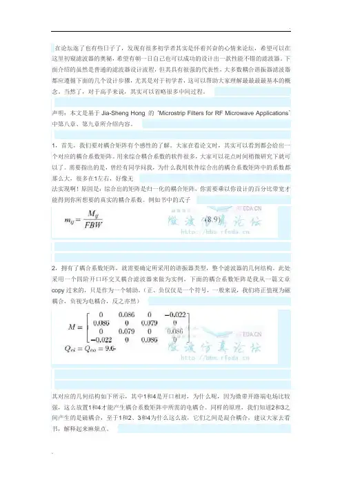
(正、负仅仅是一个符号,一般来说,我们将正值视为磁耦合,负视为电耦合,反之亦然)其对应的几何结构如下所示,其中1和4是开口相对,为什么呢,因为微带开路端电场比较强,这么放置1和4才能产生耦合系数矩阵中所需的电耦合。
同样的原理,我们知道2和3之间产生的是磁耦合,至于1和2、3和4为什么这么放,它们之间是混合耦合,建议大家去看书,解释起来麻烦点。
3,那么,谐振器之间的几何尺寸怎么确定呢?再下一步,就是用HFSS来提取两两谐振器之间的耦合系数与几何尺寸的关系了。
只有确定了所有的几何尺寸,才能建立一个滤波器的初始模型。
1)根据腔数和整体尺寸确定大致腔体尺寸2)单腔仿真,确定谐振杆和调谐杆的半径r1,r2,3)根据元件值计算理论耦合系数,然后做双腔仿真固定2)中得到的参数不变,对两腔间距W作参数扫描调整,输出K-W曲线,使得W满足K要求4)计算理论需要的Qe,再做单端口Qe仿真,调整连接引线接在谐振杆上的位置T直至符合要求5)根据以上得到的数据整体仿真6)得到的曲线很不理想,再调整获得合适的中心频率,带宽,但是通带衰减过大的问题始终无法解决随后对T调整,发现T越大反而通带衰减越小,而以前看到资料上说,中心抽头接入的位置应尽量靠近谐振杆的短路端,我现在选T=1.8mm,通带衰减最好才-13分你要用软件仿真腔体滤波器得到一个理想的结果是比较困难的,一般只要仿真出来有波形的样子,并且保证中心频率和带宽满足要求就可以加工了.一般都是能实调出来的.如果你非要在软件中调个好的波形出来,那就要不断的调整耦合以及有载Q值.其中影响最大的是K12和有载Q值,你调试的主要精力需要放在改变一二腔的距离,抽头高度,以及第一腔的加载螺钉上.过程是比较烦琐的,祝你早日成功!很多问题可以直接再论坛里搜索,比百度,好对哦了1、看下频率(因为这是后面HFSS或者CST仿真要用的单腔频率)2、看带宽和近端抑制点以及插损(这个可以用相关软件仿比如MA TLAB或者COUPLEFILA 仿真下需要几阶,几个传输零点以及交叉耦合的方式。
一般阶数越少,插损越好,抑制越插)3、再根据带宽所需要的耦合系数用HFSS或者CST仿真下,看谐振杆的间距或者耦合窗口应该定多大。
4、开始排腔,以及投入初样(一般开始做初样前还可以拿Desinger把电路仿真下,因为Desinger里面可以改变每个腔的Q值等,进行验证,看设计是否有明显的错误)5、调试,这个其实就是看个人的水平了,多动手多思考第四步排完腔一般我会用HFSS或者CST仿下Q值,看能否达到第二步用解析软件计算时预设的Q值,如果达不到就要重新考虑方案了看懂规范书抑制损耗回波功率互调温补要了解,先看通带曲线确定节数几传输零点个数零点实现形式和对应位置以及Q多少满足综合指标,仿单腔确定频率和Q值,观察几个元件间距(影响功率因素),后布局几点重要建议:布局的空间合理性和结构紧凑,生产可操作性,各个通道(单腔大小)分配均匀,功率要求尽量内部各个间距加大,互调高要对连接器表面处理材料光洁度做要求温补要考虑材料的不同环境下发生形变对指标的影响另外选用几种形式:交指梳状平行耦合,这就要看个人喜好了对于窄带滤波器来说,仿真频率必须放在中心频率上,收敛:maximum number 设置个几十,maximum delta s:0.02.看过一些资料,对耦合系数和端口外部Q值的计算都已了解,现在在仿真上有些问题,向大家请教一下第一个就是耦合会使谐振频率下降,所以仿真时会让单腔的谐振频率稍微高一些,那么一般应该高多少呢?第二个就是比如1、2两个腔的耦合窗尺寸已经调好了,耦合系数K12在中心频率和理论值差不多,接着在仿真2、3两个腔的时候,调节2、3腔之间耦合窗口大小使耦合系数K23与理论差不多的时候,谐振频率已经偏离了中心频率,这种情况接着怎么处理呢?需要调节什么参数呢?第三个就是在HFSS里用本征模仿真外部Q值的时候发现Q值与理论值一样的时候,此时的谐振频率与中心频率不一致,这种情况该如何处理呢?一,一般缩个15%~20%,原则上你能调回来就好二,改变谐振杆高度调频率啊,尽量在中心频率下算窗尺寸三,还是改变谐振杆的高度吧正耦合系数(磁耦合)可以很简单的通过腔与腔之间各种形状的开孔实现,《现代微波滤波器的结构与设计》里面有对应的相关公式。
• 126•本文介绍了基于Ansoft 公司的Ansoft Designer 微波仿真软件,在射频电路设计中进行滤波器的设计建模仿真与验证。
选取了两款具有代表性的射频无源低通滤波器,根据频率频段的不同,包括集总参数和分布参数类型的不同元件建模仿真计算优化,并通过试验电路实际测试性能指标,验证仿真结果。
50Ω阻抗匹配微带线宽。
该线宽可通过仿真软件输入滤波器工作的频率范围,板材的介电常数、板材厚度等参数即可计算得出,W=1.1mm 。
建模的原理图模型如图1所示。
2.3 仿真结果将扇形短截线的尺寸参数和连接微带线的线宽和线长参数设基于Ansoft仿真软件实现射频滤波器的设计与应用中电科仪器仪表有限公司 陈 丽图1 2GHz低通滤波器原理图模型图2 2GHz低通滤波器仿真结果图3 2GHz低通滤波器实际测量结果硬件设计人员经常需要设计各种类型的滤波器,用以滤除信号通道中不需要的信号,可以通过常规技术或软件来设计,常规技术设计困难耗时,Ansoft Designer 微波仿真软件可有效快速的实现各种滤波器的建模及参数的仿真计算,提高了设计效率。
1 滤波器的类型模拟滤波器按功能分为低通、高通、带通和带阻滤波器。
在射频电路中设计滤波器时,频率高于500MHz 的频段,由于寄生电抗,采用集总参数元件电感、电容已不合适,需要使用分布参数元件实现,因此模拟滤波器根据频段以及制作工艺又衍生出微带线滤波器。
2 2GHz低通滤波器的设计应用2.1 设计目标输入输出阻抗为50Ω,带宽为2GHz ,滤波器插入损耗小于3dB ,带内波纹小于3dB ,4GHz 的阻带抑制大于60dB 。
2.2 原理图模型由于频率高于500MHz 的滤波器难于采用分立元件实现,工作波长与滤波器元件的物理尺寸相近,造成损耗并使电路性能恶化,需将集总参数元件变换为分布参数元件,这里采用4阶扇形微带短截线通过微带线级联。
短截线的电长度以及是开路还是短路,决定了是容性还是感性,电长度通过扇形的半径、角度和短截线的宽度等参数来设置。
基于HFSS的滤波器设计流程HFSS(High Frequency Structure Simulator)是一种强大的电磁场模拟软件,可用于设计和优化各种微波和射频滤波器。
下面是基于HFSS 的滤波器设计流程,包括滤波器的初步设计、模型的创建和分析、参数优化以及最后的仿真验证。
1.滤波器的初步设计:首先确定所需滤波器的类型和规格,如低通滤波器、带通滤波器或阻带滤波器等。
根据滤波器的频带宽度、中心频率、通带损耗和阻带衰减等要求,初步选择滤波器的结构和拓扑。
2.模型的创建和分析:在HFSS中创建滤波器的几何模型。
可以使用HFSS自带的CAD工具或第三方工具创建模型,并导入到HFSS中。
确保模型的几何形状和尺寸与设计要求相符。
之后,通过HFSS进行射频电磁场模拟分析。
设置合适的频率范围,并给出合适的激励条件。
根据模型的几何形状和材料特性,计算出滤波器的S参数、功率传输和电场分布等。
3.参数优化:根据分析结果,评估滤波器的性能是否满足设计要求。
如果结果不满足要求,需要对设计参数进行优化。
通过调整滤波器的几何形状、模型的材料特性或其他设计参数,再次进行HFSS模拟。
通过反复优化,逐步改善滤波器的性能。
可以使用HFSS自带的优化工具,如参数扫描、自动优化或遗传算法等,来寻找最佳的设计参数组合。
4.仿真验证:在完成参数优化后,对滤波器进行最后的仿真验证。
使用优化后的设计参数,进行HFSS模拟分析。
通过分析结果,检查滤波器是否满足设计要求,并评估其性能。
如果滤波器性能仍然不满足要求,可以进一步优化设计参数,或者重新考虑滤波器的拓扑结构。
5.后处理和导出:在完成仿真验证后,可以进行一些后处理操作,如绘制频率响应曲线、电场分布图或功率传输图等。
这些后处理结果对于滤波器的性能评估和进一步优化非常有帮助。
最后,可以将滤波器的设计参数导出,用于后续的原理图设计和实际制造。
可以导出滤波器的尺寸数据、材料特性和优化参数等。
应用HFSS设计40 MHz腔体滤波器
王清芬;马延爽
【期刊名称】《无线电工程》
【年(卷),期】2008(38)12
【摘要】应用HFSS仿真软件设计了40 MHz的腔体滤波器,由腔间耦合系数和外界Q值的理论值,应用HFSS软件进行电磁仿真,得到腔体和耦合结构的实际结构初值,然后进行整体仿真和优化,完成整个设计.由于应用了仿真软件,使得设计简单,提高了成功率,解决了腔体滤波器在VHF频段频率低、功率大的设计难题.这种软件设计方法具有很强的通用性, 结构形式也可灵活多样,如采用了特殊的"伞状"层加载结构,大大缩小了滤波器的体积.
【总页数】3页(P44-46)
【作者】王清芬;马延爽
【作者单位】中国电子科技集团公司第五十四研究所,河北,石家庄,050081;中国电子科技集团公司第五十四研究所,河北,石家庄,050081
【正文语种】中文
【中图分类】TN454
【相关文献】
1.基于HFSS的915 MHz微带天线设计与仿真验证 [J], 吴志雄;王洪
2.基于HFSS的1800MHz同轴谐振微波介质滤波器的设计及仿真 [J], 付玉红;陈文文;闫瑞瑞;傅晶
3.100MHz-400MHz宽带双定向耦合器设计 [J], 杨青山
4.基于HFSS电容加载梳状腔体滤波器设计 [J], 肖东; 何清怡
5.基于HFSS的5G系统腔体滤波器的设计与仿真 [J], 罗兵;王钊华;邹剑萍;杨惠淇;杨露瑶;黄子玲
因版权原因,仅展示原文概要,查看原文内容请购买。