少子寿命测试判断是否有外延
- 格式:pdf
- 大小:559.86 KB
- 文档页数:4

表面复合对少子寿命测量影响的定量分析我们测量硅单晶、铸造多晶以及单晶硅片、多晶硅片的少子寿命,都希望得到与真实体寿命b τ相接近的测量值(表观寿命),而不是一个受表面影响很大的表面复合寿命s τ。
因为在寿命测量中只有b τ才能真正反映半导体材料的内在质量,而表面复合寿命只能反映样品的表面状态,是随表面状态变化而变化的变数。
通过仪器测量出的寿命值我们一般称为表观寿命,它与样品体寿命及表面复合寿命有如下关系,公式(1)由SEMI MF28-0707给出的计算公式τ0 =SF R τ--11(τ0或b τ表示体寿命)推演出来:Sb F τττ111+= (1)即仪器测量值F τ,它实际上是少子体寿命b τ和表面复合寿命s τ的并联值。
光注入到硅片表面的光生少子向体内扩散,一方面被体内的复合中心(如铁原子)复合,另一方面扩散到非光照面,被该表面的复合中心复合。
光生少子在体内平均存在的时间由体复合中心的多少而决定,这个时间就称为体寿命。
如果表面很完美,则表面复合寿命趋于无穷大,那么表观寿命即等于体寿命。
但实际上的表面复合寿命与样品的厚度及表面复合速度有关。
由MF1535-0707中给出slD l spdiff s 222+=+=πτττ (2)可知,其中: diff τ=Dl 22π——少子从光照区扩散到表面所需的时间sp τ=2ls——少子扩散到表面后,被表面(复合中心、缺陷能级)复合所需要的时间l ——样品厚度D ——少子扩散系数,电子扩散系数Dn=33.5cm 2/s ,空穴扩散系数Dp=12.4 cm 2/sS ——表面复合速度,单位cm/s硅晶体的表面复合速度随着表面状况在很大范围内变化。
如表1所示:表1据文献记载,硅抛光面在HF 酸中剥离氧化层后复合速度可低至0.25cm/s ,仔细制备的干氧热氧化表面复合速度可低至1.5-2.5cm/s ,但是要达到这样的表面状态往往不容易,也不稳定,除非表面被钝化液或氧化膜保护。
半导体少子寿命测量实验实验:半导体少子寿命的测量一.实验的目的与意义非平衡少数载流子(少子)寿命是半导体材料与器件的一个重要参数。
其测量方法主要有稳态法和瞬态法。
高频光电导衰退法是瞬态测量方法,它可以通过直接观测少子的复合衰减过程测得其寿命。
通过采用高频光电导衰退法测量半导体硅的少子寿命,加深学生对半导体非平衡载流子理论的理解,使学生学会用高频光电导测试仪和示波器来测量半导体少子寿命。
二.实验原理半导体在一定温度下,处于热平衡状态。
半导体内部载流子的产生和复合速度相等。
电子和空穴的浓度一定,如果对半导体施加外界作用,如光、电等,平衡态受到破坏。
这时载流子的产生超过了复合,即产生了非平衡载流子。
当外界作用停止后,载流子的复合超过产生,非平衡少数载流子因复合而逐渐消失。
半导体又恢复平衡态。
载流子的寿命就是非平衡载流子从产生到复合所经历的平均生存时间,以τ来表示。
下面我们讨论外界作用停止后载流子复合的一般规律。
当以恒定光源照射一块均匀掺杂的n 型半导体时,在半导体内部将均匀地产生非平衡载流子Δn 和Δp 。
设在t=0时刻停止光照,则非平衡载流子的减少-d Δp /dt 应等于非平衡载流子的复合率Δp (t )/τ。
1/τ为非平衡载流子的复合几率。
即:()τt p dt p d ?=?- (1-1)在小注入条件下,τ为常量,与Δp (t )无关,这样由初始条件:Δp (0)=(Δp )0可解得:()τt e p t p -?=?0 (1-2)由上式可以看出:1、非平衡载流子浓度在光照停止后以指数形式衰减,Δp (∝)=0,即非平衡载流子浓度随着时间的推移而逐渐消失。
2、当t=τ时,Δp (τ)=(Δp )0/e 。
即寿命τ是非平衡载流子浓度减少到初始值的1/e 倍所经过的时间。
因此,可通过实验的方法测出非平衡载流子对时间的指数衰减曲线,由此测得到少子寿命值τ。
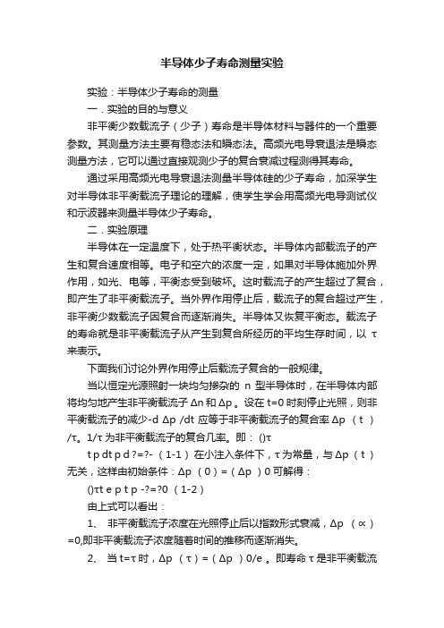
图1-1 高频光电导衰退法测量原理图高频光电导衰减法测量原理如图1-1所示。

施美乐博公司上海代表处上海浦东新区商城路738号胜康廖氏大厦906A (邮编:200120Rm.906A,Suncome Liauw's Plaza, No.738, Shangcheng Road,Pudong,Shanghai 200120, ChinaTel: +86-21-58362889 Fax: +86-21-58362887To : Semilab 产品用户FROM : 黄黎 / Semilab Shanghai Office Pages : 5 Pages (included this page Refer : 1、Semilab 公司上海办事处联系方法2、关于少子寿命测试若干问题的讨论尊敬的Semilab 产品用户:感谢您和贵公司一直以来对我们的支持!为了更好地服务于中国客户,Semilab 公司现已在上海成立办事处。
具体的联系方法为:施美乐博公司上海办事处上海浦东新区商城路738号胜康廖氏大厦906A (邮编:200120Tel: +86-21-58362889 Fax: +86-21-58362887联系人:黄黎先生手机: +86-138******** (Shanghai +86-135******** (Beijing E-mail:leon.huang@ Website: 现提供关于少子寿命测试若干问题的讨论,供您参考,并烦请填写客户意见反馈表,传真给我们,以便我们改进工作,谢谢!如您还有任何问题或需要,请随时与我们联系。
此致敬礼!施美乐博公司上海办事处 2006年4月7日施美乐博公司上海代表处上海浦东新区商城路738号胜康廖氏大厦906A (邮编:200120Rm.906A,Suncome Liauw's Plaza, No.738, Shangcheng Road,Pudong,Shanghai 200120, ChinaTel: +86-21-58362889 Fax: +86-21-58362887关于少子寿命测试若干问题的讨论鉴于目前Semilab 少子寿命测试已在中国拥有众多的用户,并得到广大用户的一致认可。

类单晶少子寿命浅析一、少子寿命的概念处于热平衡状态下的半导体,在一定温度下,载流子的浓度是一定的,称为平衡载流子浓度,如果对半导体施加外界作用,破坏了热平衡的条件,称为非平衡状态。
比平衡状态多出来的这部分载流子称为非平衡载流子。
非平衡载流子分为非平衡多数载流子和非平衡少数载流子,对于n型半导体材料,多出来的电子就是非平衡多数载流子,空穴则是非平衡少数载流子,对p型半导体材料则相反。
产生非平衡载流子的外界作用撤除以后,它们要逐渐衰减以致消失,最后载流子浓度恢复到平衡时的值,非平衡载流子的平均生存时间称为非平衡少数载流子的寿命,简称少子寿命。
二、少子寿命的测试原理我们采用的是微波光电导衰退法测试少子寿命,主要包括激光注入产生电子-空穴对和微波探测信号这两个过程。
904nm的激光注入(对于硅,注入深度大约为30um)产生电子-空穴对,导致样品电阻率增加,当撤去外界光时,电阻率随时间指数衰减,这一趋势间接反映少数载流子的衰减趋势,从而通过微波探测电导率随时间变化的趋势就可以得到少数载流子的寿命。
三、硅片钝化前后的少子寿命对比下面对P0090098号锭钝化前后的少子寿命进行分析:A01-1(前)1.174图1 A01钝化前后的少子寿命对比图2 B10钝化前后少子寿命对比图3 C09钝化前后少子寿命对比从上面三个图可以看出钝化前后少子寿命差别很大,钝化前少子寿命<1的硅片,钝化后少子寿命<3us;钝化前少子寿命>1的硅片,钝化后最高可达到38us,这说明钝化前的少子寿命只能代表一种趋势,不能反映硅片的真实少子寿命。
因为单多晶裸硅片若不经过清洗钝化,硅片表面复合中心占主导地位,掩盖了光照对体少子寿命的影响,因此对不经过清洗、钝化的裸硅片,无法确定少子寿命与光照时间的对应关系,也就无法判断硅片的质量。
下图分别为A01、B10、C09钝化前后少子寿命值趋势的对比情况:图4 钝化前后少子寿命值趋势对比从上图可以看出(1)钝化前、后的少子寿命趋势并不完全一致,钝化前少子寿命高的,钝化后不一定高。

少子寿命测试实验报告一、实验目的和任务1、了解光电导法测试少数载流子寿命的原理,熟练掌握LTX2高频光电导少数载流子寿命测试仪的使用方法;2、测非平衡载流子的寿命。
二、实验原理处于热平衡状态的半导体,在一定温度下,载流子浓度是一定的。
这种处于热平衡状态下的载流子浓度,称为平衡载流子浓度。
半导体的热平衡状态是相对的,有条件的。
如果对半导体施加外界作用,破坏了热平衡的条件,这就迫使它处于与热平衡状态相偏离的状态,称为非平衡状态。
处于非平衡状态的半导体,其载流子浓度不再是X和X,可以比它们多出一部分。
比平衡状态多出来的这部分载流子称为非平衡载流子,有时也称过剩载流子。
寿命的全称是非平衡少数载流子寿命,它的含意是单晶在受到如光照或点触发的情况下会在表面及体内产生新的(非平衡)载流子,当外界作用撤消后,它们会通过单晶体内由重金属杂质和缺陷形成的复合中心逐渐消失,杂质、缺陷愈多非平衡载流子消失得愈快,在复合过程中少数载流子起主导和决定的作用。
这些非平衡少数载流子在单晶体内平均存在的时间就简称少子寿命。
通常寿命是用实验方法测量的。
各种测量方法都包括非平衡载流子的注入和检测两个基本方面。
最常用的注入方法是光注入和电注入,而检测非平衡载流子的方法很多。
不同的注入和检测方法的组合就形成了许多寿命测量方法。
三、实验设备本实验采用LTX2高频光电导少数载流子寿命测试仪。
该仪器灵敏度高,配备有红外光源,可测量包括集成电路级硅单晶在内的各种类型硅单晶及常用的晶体管级锗单晶。
该仪器根据国际通用方法—高频光电导衰退法的原理设计,由稳压电源、高频源、检波放大器、脉冲光源及样品电极共五部分组成,采用印刷电路和高频接插件连接。
整机结构紧凑,测量数据准确、可靠。
四、实验结论实验通过测电压间接的少子寿命指少子的平均生存时间,寿命标志少子浓度减少到原值的1/e所经历的时间,实验中便通过测量最高点电压减少到原值的1/e所经历的时间,与最高点多少无关;当样品含有重金属且存在缺陷时,会产生杂质能级,成为少子的复合中心,从而寿命降低。
少子寿命测试及表面处理和钝化方法解析少子寿命测试及表面处理和钝化方法解析少数载流子寿命(简称少子寿命)是半导体材料的一项重要参数,它对半导体器件的性能、太阳能电池的效率都有重要的影响,少子寿命高的话,电池效率相应的也高一点,少子寿命低的话,电池效率也会相应的变低。
鉴于目前 Semilab 少子寿命测试已在中国拥有众多的用户,并得到广大用户的一致认可。
现就少子寿命测试中,用户反映的一些问题做出如下说明,供您在工作中参考:1、Semilabμ-PCD 微波光电导少子寿命的原理微波光电导衰退法(Microwave photoconductivity decay)测试少子寿命,主要包括激光注入产生电子-空穴对和微波探测信号的变化这两个过程。
904nm 的激光注入(对于硅,注入深度大约为30um)产生电子-空穴对,导致样品电导率的增加,当撤去外界光注入时,电导率随时间指数衰减,这一趋势间接反映少数载流子的衰减趋势,从而通过微波探测电导率随时间变化的趋势就可以得到少数载流子的寿命。
少子寿命主要反映的是材料重金属沾污及缺陷的情况。
Semilab μ-PCD 符合ASTM 国际标准F 1535 - 002、少子寿命测试的几种方法通常少数载流子寿命是用实验方法测量的,各种测量方法都包括非平衡载流子的注入和检测两个基本方面。
最常用的注入方法是光注入和电注入,而检测非平衡载流子的方法很多,如探测电导率的变化,探测微波反射或透射信号的变化等,这样组合就形成了许多寿命测试方法。
近30 年来发展了数十种测量寿命的方法,主要有:直流光电导衰退法;高频光电导衰退法;表面光电压法;少子脉冲漂移法;微波光电导衰减法等。
对于不同的测试方法,测试结果可能会有出入,因为不同的注入方法,表面状况的不同,探测和算法等也各不相同。
因此,少子寿命测试没有绝对的精度概念,也没有国际认定的标准样片的标准,只有重复性,分辨率的概念。
对于同一样品,不同测试方法之间需要作比对试验。
太阳能电池硅片少子寿命的测试
首先,测量载流子寿命是一种常见的方法,通过暗态下的载流子寿命测量来评估材料的质量。
这种方法可以使用不同的技术,如微波探测、激光探测和电学探测等,来确定材料中电子和空穴的寿命。
其次,表面重复率是另一种常用的测试方法,它通过测量材料表面上的载流子寿命来评估材料的质量。
这种方法可以帮助确定材料表面的质量和制备工艺的稳定性。
最后,微波电容是一种用来测量材料中载流子寿命的方法,通过测量材料对微波的响应来评估载流子的寿命。
这种方法对于大面积的样品测试非常有效,并且可以提供关于材料质量和性能稳定性的重要信息。
总之,测试太阳能电池硅片少子寿命是评估太阳能电池材料质量和性能稳定性的关键步骤,可以通过测量载流子寿命、表面重复率和微波电容等方法来全面评估材料的质量和性能。
这些测试方法可以帮助太阳能电池制造商和研究人员确定材料的质量,并改进制备工艺,从而提高太阳能电池的效率和稳定性。
高频光电导衰减法测量Si 中少子寿命预习报告:一,什么是少子寿命?少子,即少数载流子。
少子寿命指少子的平均生存时间,寿命标志少子浓度减少到原值的1/e 所经历的时间。
少数载流子寿命是与半导体中重金属含量、晶体结构完整性直接有关的物理量。
它对半导体太阳电池的换能效率、半导体探测器的探测率和发光二极管的发光效率等都有影响。
二,如何测量少子寿命?测量非平衡少数载流子寿命的方法有许多种,分别属于瞬态法和稳态法两大类。
本实验采用高频光电导衰减法测量Si 中少子寿命。
三,实验原理:当能量大于半导体禁带宽度的光照射样品时,在样品中激发产生非平衡电子和空穴。
若样品中没有明显的陷阱效应,那么非平衡电子(∆n )和空穴(∆p)的浓度相等,它们的寿命也就相同。
样品电导率的增加与少子浓度的关系为n q p q n p ∆+∆=∆μμσ当去掉光照,少子密度将按指数衰减,即τtep -∝∆,因此导致电导率为τσte-∝∆。
高频源提供的高频电流流经被测样品,当红外光源的脉冲光照射样品时,单晶体内产生的非平衡光生载流子使样品产生附加光电导,从而导致样品电阻减小。
由于高频源为恒压输出,因此流经样品的高频电流幅值增加∆I ,光照消失后,∆I 逐渐衰减,其衰减速度取决于光生载流子在晶体内存在的平均时间,即寿命。
在小注入条件下,当光照区复合为主要因素时,∆I 将按指数规律衰减,此时取样器上产生的电压变化∆V 也按同样的规律变化,即τte V V -∆=∆0图2指数衰减曲线一,Si.t∆V~t 曲线:(一)(二)(三)计算少子寿命:电压满足τteV V -∆=∆0,在测量数据中,由于时间原点的不同选择,t 的绝对值不同,但是相对值相同。
任选两个点( ),( ),有,,两式相除,得。
对第一组数据,取(4.26E-5s,0.298V),(8.06E-5s,0.094V)。
利用上述公式得。
对第二组数据,取(4.44E-5s,0.622V),(7.44E-5s,0.222V)。
Abruptness of a-Si:H/c-Si interface revealed by carrier lifetime measurementsStefaan De Wolf and Michio KondoCitation: Appl. Phys. Lett. 90, 042111 (2007); doi: 10.1063/1.2432297View online: /10.1063/1.2432297View Table of Contents: /resource/1/APPLAB/v90/i4Published by the AIP Publishing LLC.Additional information on Appl. Phys. Lett.Journal Homepage: /Journal Information: /about/about_the_journalTop downloads: /features/most_downloadedInformation for Authors: /authorsAbruptness of a-Si:H/c-Si interface revealed by carrierlifetime measurementsStefaan De Wolf a͒and Michio KondoNational Institute of Advanced Industrial Science and Technology(AIST),Central2,1-1-1Umezono,Tsukuba,Ibaraki305-8568,Japan͑Received27September2006;accepted15December2006;published online26January2007͒Intrinsic hydrogenated amorphous siliconfilms can yield outstanding electronic surface passivation of crystalline silicon wafers.In this letter the authors confirm that this is strongly determined by the abruptness of the interface.For completely amorphousfilms the passivation quality improves by annealing at temperatures up to260°C,most likely byfilm relaxation.This is different when an epitaxial layer has been grown at the interface duringfilm deposition.Annealing is in such a case detrimental for the passivation.Consequently,the authors argue that annealing followed by carrier lifetime measurements allows determining whether the interface is abrupt.©2007American Institute of Physics.͓DOI:10.1063/1.2432297͔Hydrogenated amorphous silicon͑a-Si:H͒films depos-ited on crystalline silicon͑c-Si͒surfaces have increasingly attracted attention over the past20years.Initially,it was discovered that abrupt electronic heterojunctions can be cre-ated with such structures.1Soon afterwards applications fol-lowed,including bipolar transistors,2imaging devices,3and solar cells.4For the latter it was recognized that the output parameters benefit substantially from inserting a few nano-meter thin intrinsic a-Si:H͑i͒film between the doped amor-phous emitter and c-Si substrate.For solar cells that feature a similar heterostructure back surfacefield,impressive energy conversion efficiencies exceeding21%have been reported.5 The role of the a-Si:H͑i͒buffer layer has been discussed in literature͑see,e.g.,Refs.6–12͒:It is known that suchfilms can yield outstanding surface passivation for c-Si surfaces,13 but also that growth of an epitaxial interface during a-Si:H͑i͒deposition is detrimental for heterojunction device performance.12For hot wire chemical vapor deposited ͑CVD͒a-Si:H,where no ion bombardment takes place, abrupt interfaces have been obtained either by limiting the deposition temperature T depo͑Ref.14͒or by terminating the c-Si surface with a SiN x monolayer prior to a-Si:Hdeposition.15The abruptness of the interface,i.e.,whetherinstant a-Si:H deposition on c-Si occurred without initialepitaxial growth,was in these studies determined either bytransmission electron microscopy͑TEM͒͑Refs.12,14,and15͒or by͑in situ͒spectroscopic ellipsometry͑SE͒,16forwhich mirror polished surfaces are desirable.To gain know-ledge about the electronic surface passivation properties ofthese interfaces,the most straightforward technique is bymeasuring the effective carrier lifetimeeff of the samples. Such measurements are known to be extremely sensitive, allowing for detection of bulk defect densities as low as 109–1011cm−3in a simple,contactless technique at room temperature.17In this letter,we show that by low temperature͑up to260°C͒postdeposition annealing,the surface passivationquality of direct plasma enhanced͑PE͒CVD a-Si:H͑i͒films improves when the a-Si:H/c-Si interface is abrupt.This contrasts with the case when an epitaxialfilm has been grown at the interface,where the surface passivation quality is seen to degrade significantly by a similar annealing treat-ment.Consequently,we argue that annealing followed by carrier lifetime measurements allows accurate determination of the onset of epitaxial growth in an easy-to-use way which is not restricted to polished c-Si surfaces.For the experiments,300m thick relatively low resistivity͑ϳ3.0⍀cm͒boron-dopedfloat zone͑100͒͑FZ͒-Si͑p͒wafers have been used.Both surfaces of the sub-strates were mirror polished to eliminate the influence of substrate surface roughness on the passivation properties18 and to allow for SE measurements.For predeposition surface cleaning,the samples werefirst immersed in a ͑H2SO4:H2O2͒͑4:1͒solution for10min to grow a chemical oxide,which was followed by a rinse in de-ionized water. The oxide was then stripped off in a dilute HF solution͑5%͒for30s.After this the samples were immediately transferred to the load lock of the deposition system.Forfilm deposi-tion,a parallel plate direct PECVD reactor operated at radio frequency͑rf͒͑13.56MHz͒power was used,in which the samples were mounted at the top electrode.The electrode distance and diameter were respectively20and230mm.An undiluted SiH4flow of20SCCM͑SCCM denotes cubic cen-timeter per minute at STP͒was used and the chamber was maintained at low pressure͑0.5Torr͒.The value for T depo was varied from105to255°C.The rf power absorbed by the plasma was5W.This is the minimal power required to maintain a stable plasma at the given deposition conditions. To evaluate the surface passivation quality,identicalfilms of about50nm thick were deposited on both wafer surfaces. After deposition,the samples were consecutively annealed in a vacuum furnace͑30min,with annealing temperatures T ann ranging from120to260°C͒.In between the annealing steps,the value foreff of the samples was measured with a Sinton Consulting WCT-100quasi-steady-state photocon-ductance system,19operated in the so-called generalized mode.Since high quality FZ-Si wafers have been used throughout the experiments,the contribution of the bulk to the total recombination expressed byeff can be neglected.In such a case,the effective surface recombination velocity S eff, which value can be regarded as a direct measure for the passivation quality of thefilms present at the surfaces,maya͒Electronic mail:stefaan.dewolf@aist.go.jpAPPLIED PHYSICS LETTERS90,042111͑2007͒0003-6951/2007/90͑4͒/042111/3/$23.00©2007American Institute of Physics90,042111-1be approximated by S eff =d *͑2eff ͒−1,with d being the wafer thickness.17All reported values for eff and S eff are evaluated at a constant minority carrier injection density,⌬n ,of 1.0ϫ1015cm −3.The thickness of the deposited films was ex situ determined by measuring ellipsometry spectra ͑,⌬͒using a Woollam M-2000rotating-compensator instrument.In order to verify the SE analyses,high-resolution ͑HR ͒cross-sectional TEM micrographs were acquired by a Jeol JEM2000EX system operated at an acceleration voltage of 200kV.Figure 1shows the imaginary part of the pseudodielec-tric function 20͗1͘+i ͗2͘of thin a -Si:H ͑i ͒films on c -Si wa-fers obtained from SE measurements at the initial deposition stages ͑here after 108s ͒and for different values of T depo .For reference,data for bare c -Si are given too.The figure dis-plays how samples featuring films for which T depo ജ205°C ͑group a in Fig.1͒show an evident crystalline signature,suggesting that those films were epitaxially grown.Con-versely,for samples with films for which T depo ഛ180°C ͑group b ͒,the value for ͗2͘deviates significantly from that of bare c -Si substrates,leading us to conclude that these films are most likely amorphous,as expected.Figure 2re-veals how the surface passivation quality of similar films,again for different values of T depo ,changes as a function of T ann .For the films deposited at the lowest temperature ͑T depo =105°C ͒,initially the passivation is poor,but im-proves to a remarkable extent by annealing.The surface pas-sivation quality of as-deposited films improves with higher T depo up to 180°C.Postannealing up to 260°C increases the values for eff further,well in excess of 1ms.This situation is different for films deposited at 205°C,where annealing does not give rise anymore to an improvement,and for even higher values of T depo ,the figure shows that the passivation quality actually drastically goes down.Figure 3shows how the onset of epitaxial film growth and the phenomenon where postannealing of the samples results in passivation losses are related to each other.Part ͑a ͒of this figure gives the a -Si:H ͑i ͒film thickness,d bulk ,during the initial deposition stages,as function of T depo .These data are obtained from fitting the measured SE data of the different samples to a two-layer model,to take surface roughness on top of the a -Si:H film into account ͓see the inset in Fig.3͑a ͔͒.For allfilms deposited at T depo ജ205°C,hardly any film growth can be observed with SE during at least the first 72s.The difficulty to fit the initial film thickness to the SE data sug-gests that for the complete surface the deposited material is crystalline.21This area is crosshatched in the figure.From the slopes of the exponential fits in the Arrhenius plot as given in Fig.2,an activation energy E A can be extracted.This is given in Fig.3͑b ͒as function of T depo .The area with negative values for E A coresponds to films for which postannealing is harmful for the passivation quality and has been cross-hatched in the figure too.A good correspondence exists be-tween the onset where crystalline material is grown at the full interface during film deposition and the point where the value of E A becomes negative.Figure 4shows aHRTEMFIG.1.͑Color online ͒Imaginary part of the pseudodielectric function ͗⑀1͘+i ͗2͘for thin a -Si:H ͑i ͒films deposited at different temperatures on c -Si surfaces,obtained from ͑ex situ ͒SE measurements.The deposition time for all films was 108s.Group a shows data of samples featuring films with T depo ജ205°C,whereas for group b,T depo ഛ180°C.For reference,data for a bare c -Si substrate are giventoo.FIG.2.͑Color online ͒Influence of the postdeposition annealing temperature T ann on the surface passivation quality for PECVD a -Si:H ͑i ͒films deposited at different temperatures T depo .All deposition times were 12min,whereas annealing times were 30min.Starting from the T ann onset of annealing induced passivation changes,the shown lines are exponential fits of thedata.FIG.3.͑a ͒Calculated film thickness d bulk from ex situ SE measurements as function of T depo ,given for several deposition times t depo .The used two-layer model is shown in the inset.Crosshatched area shows films with epitaxially grown interface.͑b ͒Extracted activation energy E A as function of T depo for the films shown in Fig.2.Crosshatched area shows films for which the surface passivation degrades by annealing.The lines are guides for the eye.micrograph of one of the a -Si:H ͑i ͒/c -Si interfaces of the sample with films deposited at 230°C,as indicated in Fig.3͑b ͒.This micrograph confirms that indeed a substantial part of the film was epitaxially grown.The interpretation of E A may be that it represents an energy barrier for a relaxed a -Si:H ͑i ͒/c -Si interface.Since E A is extracted from eff measurements,its value will mainly be determined by the density of electronically active defects of the film.These are the defects that are within reach of the c -Si minority carrier wave function.The impact of these de-fects is determined by their energetic position within the band gap and their electron and hole capture cross sections.This contrasts with electron spin resonance ͑ESR ͒measure-ments of a -Si:H ͑i ͒layers,which rather reveal paramagnetic defect densities in the bulk of relatively thick ͑typically a few micrometers ͒films deposited on quartz substrates.Nev-ertheless,for 4m thick films deposited at 25°C,Biegelsen et al.observed in their ESR studies activation energies of about 0.5eV for the decrease of the Si dangling bond density by postdeposition annealing at values for T ann up to 250°C.22Considering the differences in measurement tech-niques,a good correspondence exists between this value for E A and the ones obtained from eff measurements for the films deposited at low T depo as presented in Fig.3͑b ͒.From this it must be concluded that for completely amorphous films deposited on c -Si surfaces,most likely amorphous net-work relaxation is taking place during the low temperature anneal,without any bond rupture,but which is capable of annealing out defects that are harmful for the passivation quality of the films.Consequently,films with E A =0eV cor-respond to fully relaxed a -Si:H/c -Si interfaces.The shift of the optimal value for T depo from about 205°C before anneal-ing to about 155°C after annealing ͑as seen in Fig.2͒may originate from a competition between a higher hydrogen content and a relaxed film network for high quality surface passivation.The origin of negative E A values for epitaxially grown interfaces is at present less understood.Since the applied annealing temperatures must be considered to be too low for Si–H bond rupture,a possible explanation may be that for as-grown epitaxial films,most of the hydrogen at the inter-face is not bonded but present as atomic H +,perhaps yielding field effect passivation of the surface rather than physicalinterface passivation.Subsequent annealing then leads to fast H +diffusion away from the interface into the c -Si matrix,resulting in passivation losses:e.g.,for an anneal at 260°C for 30min,whereas in a -Si:H ͑with D 0=1.17ϫ10−2cm 2s −1and E a =1.53eV ͒23the hydrogen diffu-sion depth is in the order of nanometers,in c -Si ͑with D 0=1.45ϫ10−3cm 2s −1and E a =0.497eV ͒24this is about five orders of magnitude larger.D 0is the preexponen-tial term,E a is the activation energy,and k is the Boltzmann constant in the expression for the diffusivity D ͑T ͒=D 0exp ͑−E a /kT ͒.In conclusion,in this letter we have shown that high quality passivation for c -Si by means of direct PECVD a -Si:H ͑i ͒deposition has a sharp processing boundary which is defined by epitaxial growth conditions.In the case that the interface is abrupt,the deposited films benefit tremendously from a low temperature anneal,which is believed to yield film relaxation.Moreover,we argued that annealing followed by carrier lifetime measurements is a valuable tool,which is not restricted to surfaces that are mirror polished,to deter-mine the abruptness of the c -Si/a -Si:H ͑i ͒interface.1H.Matsuura,T.Okuno,H.Okushi,and K.Tanaka,J.Appl.Phys.55,1012͑1984͒.2J.Symons,M.Ghannam, A.Neugroschel,J.Nijs,and R.Mertens,Solid-State Electron.30,1143͑1987͒.3H.Mimura and Y .Hatanaka,J.Appl.Phys.61,2575͑1987͒.4M.Tanaka,M.Taguchi,T.Matsuyama,T.Sawada,S.Tsuda,S.Nakano,H.Hanafusa,and Y .Kuwano,Jpn.J.Appl.Phys.,Part 131,3518͑1992͒.5M.Taguchi, A.Terakawa, E.Maruyama,and M.Tanaka,Prog.Photovoltaics 13,481͑2005͒.6M.W.M.van Cleef,J.K.Rath,F.A.Rubinelli,C.H.M.van der Werf,R.E.I.Schropp,and W.F.van der Weg,J.Appl.Phys.82,6089͑1997͒.7M.Taguchi,K.Kawamoto,S.Tsuge,T.Baba,H.Sakata,M.Morizane,K.Uchihashi,N.Nakamura,S.Kiyama,and O.Oota,Prog.Photovoltaics 8,503͑2000͒.8N.Jensen,R.M.Hausner,R. B.Bergmann,J.H.Werner,and U.Rau,Prog.Photovoltaics 10,1͑2002͒.9M.Schmidt,A.Schoepke,L.Korte,ch,and W.Fuchs,J.Non-Cryst.Solids 338,211͑2004͒.10H.Fujiwara and M.Kondo,Appl.Phys.Lett.86,032112͑2005͒.11S.De Wolf and G.Beaucarne,Appl.Phys.Lett.88,022104͑2006͒.12T.H.Wang,E.Iwaniczko,M.R.Page,D.H.Levi,Y .Yan,H.M.Branz,and Q.Wang,Thin Solid Films 501,284͑2006͒.13S.Dauwe,J.Schmidt,and R.Hezel,in Proceedings of the 29th IEEE Photovoltaic Specialists Conference ,New Orleans,Louisiana ͑IEEE,Pis-cataway,NJ,2002͒,p.1246.14J.Thiesen, E.Iwaniczko,K.M.Jones, A.Mahan,and R.Crandall,Appl.Phys.Lett.75,992͑1999͒.15Y .Yan,M.Page,T.H.Wang,M.M.Al-Jassim,H.M.Branz,and Q.Wang,Appl.Phys.Lett.88,121925͑2006͒.16D.H.Levi,C.W.Teplin,E.Iwaniczko,Y .Yan,T.H.Wang,and H.M.Branz,J.Vac.Sci.Technol.A 24,1676͑2006͒.17D.K.Schroder,Semiconductor Material and Device Characterization ,3rd ed.͑Wiley-Interscience,Hoboken,NJ,2006͒.18S.De Wolf,G.Agostinelli,G.Beaucarne,and P.Vitanov,J.Appl.Phys.97,063303͑2005͒.19R.A.Sinton and A.Cuevas,Appl.Phys.Lett.69,2510͑1996͒.20G.E.Jellison,in Handbook of Ellipsometry ,edited by H.G.Tompkins and E.A.Irene ͑Springer,Heidelberg,2005͒.21H.Fujiwara and M.Kondo,Appl.Phys.Lett.90,013503͑2007͒.22D.K.Biegelsen,R.A.Street,C.C.Tsai,and J.C.Knights,Phys.Rev.B 20,4839͑1979͒.23D.E.Carlson and C.W.Magee,Appl.Phys.Lett.33,81͑1978͒.24C.Herring,N.M.Johnson,and C.G.Van de Walle,Phys.Rev.B 64,125209͑2001͒.FIG.4.HRTEM micrograph of one of the interfaces of the sample deposited at 230°C as indicated in Fig.3.The PECVD a -Si:H ͑i ͒film was deposited on a mirror polished c -Si ͑100͒surface.The deposition time was 12min.。