MT6189 application introduction
- 格式:pdf
- 大小:107.41 KB
- 文档页数:9

UM11817Introduction to 18-cell slider battery pack emulatorRev. 1 — 17 February 2023User manualIntroduction to 18-cell slider battery pack emulatorIntroduction to 18-cell slider battery pack emulator 1 IntroductionThe BATT-18EMULATOR board can emulate a multi-cell battery pack that can be easily hooked-up to the evaluation boards for MC33774 18-cell battery cell controllers (BCCs):•RD33774ADSTEVB - distributed board with single MC33774•RD33774CNT3EVB - centralized board with three MC33774The user can connect the BATT-18EMULATOR board for a quick evaluation of NXP BCC ICs, or to help the users in their software development. These boards basically provide a very intuitive way:•To change the voltage across any of the 18 cells of an emulated battery pack•To change the voltage across some analog inputs of the BCC IC that are typically used as temperature sensorsFigure 1. BATT-18EMULATOR2 Getting started2.1 Kit contents/packing listThe kit contents include:•BATT-18EMULATOR, 18-cell slider battery pack emulator•25 W AC-DC adapter with +5 VDC/5 A single output - DC plug type P1J (2.1 × 5.5 × 11 mm), tuning fork type, center positive•Adapter cable DC plug 2.1 × 5.5 × 11 mm to 2.5 × 5.5 × 9.5 mmIntroduction to 18-cell slider battery pack emulator 3 Getting to know the hardware3.1 Board features•18 slider potentiometers to adjust the cells voltage between 1.2 V and 3.3 V. The maximum total voltage has been limited to 60 V.•Three cells voltage can be inverted to apply voltages from −1.2 V to −3.3 V•Maximum current capability per channel: 200 mA•Three connectors for MC33774 evaluation boards connections•Temperature sensor output voltage can vary from 0 V to +4.95 V to simulate negative temperature coefficient (NTC) sensor3.2 Board functionsThe board has been designed and optimized for the operating conditions described in Table 1 and Table 2. Usage of the board beyond these conditions can lead to malfunction and damage.Table 1. Limiting valuesIn accordance with the Absolute Maximum Rating System (IEC 60134).[1]The maximum input supply current depends on the setup: number of boards connected, cells voltage, activated cell balancing channels; seeSection 3.3.3.[1]With jumpers setting, it is possible to get negative voltages from −3.3 V to −1.2 V for cells 13, 8 and 4; see Section 3.3.4.Introduction to 18-cell slider battery pack emulator 3.3 Board functional descriptionFigure 2. BATT-18EMULATOR board elements3.3.1 DescriptionEach cell emulation is made of a 5 V to 5 V unregulated isolated DC-DC converter and an adjustable regulator. The regulator output voltage is set thanks to a voltage slider. Minimum voltage is 1.2 V and maximum is set to 3.3 V.3.3.2 Connection and configurationThe emulator board requires a 5 V DC power supply with 5 A current capability. The power supply is connected to the board via J3 a Ø2.5 mm jack connector or using the 2 mm bananas J2(+) and J1(−). The center pinis connected to the positive voltage and the ring terminal to the ground. The input of the board is 5 A fuse protected. An LED allows the user to check that the board is powered up. If the voltage is present on the jack connector but the LED is off, then check the fuse F1.Up to three evaluation boards RD33774ADSTEVB or one RD33774CNT3EVB can be connected using connectors J4, J5, and J6 with no specific order.3.3.3 Current consumptionThe slider pack should be supplied with a +5 V AC-DC adapter or with a lab supply. The required supply current depends on several parameters described below.With no board connected, the default supply current on the 5 V primary is around 500 mA [19 × 28 mA (DC-DC typ supply current)].One RD33774ADSTEVB board, communicating, no balancing activated, consumes around 10.5 mA. Then the total supply current required on the 5 V primary is around 700 mA [500 mA + (19 × 10.5 mA)].If three boards are connected, then the supply current is 500 mA + (3 × 19 × 10.5 mA) = 1 A.If cell balancing is activated, the primary current depends on the cell voltage, the balancing resistance, and the number of balancing metal-oxide-semiconductor field-effect transistor (MOSFET) activated.Introduction to 18-cell slider battery pack emulator On RD33774ADSTEVB, the balancing resistance is 22 Ω per cell balancing channel. With V cell = 3.3 V, the peak balancing current is 150 mA peak, 75 mA average assuming a 50 % duty cycle. If N cell balancing MOSFETs are activated, then N × 75 mA are added to the primary current needed. If one board is connected and all18 cell balancing MOSFETs are activated, then the total current is 700 mA + 18 × 75 mA = 2 A. Each individual channel (200 mA of current capability) has to provide 10.5 mA + 75 mA averaged or 10.5 mA + 150 mA peak. Note: The current is limited to 180 mA per channel. If several boards are connected, it is recommended toavoid to activate same cell balancing channels at the same time on all the boards.3.3.4 Cell polarity selectionThree pairs of jumpers allow the polarity to be reversed for cell polarities for cell4 (C5M − C4M), cell8(C9M − C8M) and cell13 (C14M − C13M) therefore providing voltages between −1.2 V and −3.3 V; see Table 3.Note: Jumper selections should be done prior to supplying the BATT-18EMULATOR. Adjacent cell voltages are impacted when changing the polarities.3.3.5 External voltage injectionThe three jumpers can also be used as injection points to inject voltages above slider ranges: −1.2 V < V inj <+1.2 V or 3.3 V < V inj, typically to evaluate MC33774 cell terminal measurements at very low voltage (busbars) or a high-voltage cell.As example, to inject a voltage between C5M and C4M, remove jumper J8, keep jumper J7 1-2, and connect a floating supply between J8-2 and J7-1 or 2. Do not exceed maximum ratings and keep cell voltage in the range −5 V to +5 V.3.3.6 Temperature sensor simulationA separate slider allows the variation of the voltage across the temperature sensors.The temperature sensor output voltage can vary from 0 V to +4.95 V. It can mimic the temperaturevariation from −48 °C to +200 °C of a 10 kΩ NTC sensor. This output voltage is connected to four different general‑purpose input/output (GPIO) on the MC33774 (GPIO 1, 2, 7, 8) configured as ratiometric inputs with10 kΩ pull‑up resistors to VAUX (3.3 V typ.).3.4 MC33774 board connectionsThree 32 pins connectors (JAE Electronics MX34032NF2) J4, J5, J6 are connected in parallel as perthe following schematic Figure 3. Up to three boards (for example, RD33774ADSTEVB) or one boardRD33774CNT3EVB can be connected on any of these connectors.Introduction to 18-cell slider battery pack emulator Slider cell 0 is setting the voltage between C0M (cell0M) and C1M (cell0P), slider cell 1 is setting the voltage between C1M (cell1M) and C2M (cell1P), and so on, slider cell 17 is setting the voltage between C17M(cell17M) and C17P (cell17P).C17P-PWR and GND (pin 21) are used to supply the RD33774ADSTEVB and are separated from C17P andC0M respectively to avoid any voltage drop due to the current consumption of the evaluation boards.The slide temperature sensor is connected on pin 17 to pin 20 (NTC1, 2, 7 and 8 for RD33774DSTEVB).Figure 4. BATT-18EMULATOR connected to three RD33774DSTEVBIntroduction to 18-cell slider battery pack emulator 4 SchematicFigure 5. SchemaIntroduction to 18-cell slider battery pack emulator 5 Legal information5.1 DefinitionsDraft — A draft status on a document indicates that the content is still under internal review and subject to formal approval, which may resultin modifications or additions. NXP Semiconductors does not give any representations or warranties as to the accuracy or completeness of information included in a draft version of a document and shall have no liability for the consequences of use of such information.5.2 DisclaimersLimited warranty and liability — Information in this document is believed to be accurate and reliable. However, NXP Semiconductors does not give any representations or warranties, expressed or implied, as to the accuracy or completeness of such information and shall have no liability for the consequences of use of such information. NXP Semiconductors takes no responsibility for the content in this document if provided by an information source outside of NXP Semiconductors.In no event shall NXP Semiconductors be liable for any indirect, incidental, punitive, special or consequential damages (including - without limitation -lost profits, lost savings, business interruption, costs related to the removal or replacement of any products or rework charges) whether or not such damages are based on tort (including negligence), warranty, breach of contract or any other legal theory.Notwithstanding any damages that customer might incur for any reason whatsoever, NXP Semiconductors’ aggregate and cumulative liability towards customer for the products described herein shall be limited in accordance with the Terms and conditions of commercial sale of NXP Semiconductors.Right to make changes — NXP Semiconductors reserves the right to make changes to information published in this document, including without limitation specifications and product descriptions, at any time and without notice. This document supersedes and replaces all information supplied prior to the publication hereof.Applications — Applications that are described herein for any of these products are for illustrative purposes only. NXP Semiconductors makes no representation or warranty that such applications will be suitable for the specified use without further testing or modification.Customers are responsible for the design and operation of their applications and products using NXP Semiconductors products, and NXP Semiconductors accepts no liability for any assistance with applications or customer product design. It is customer’s sole responsibility to determine whether the NXP Semiconductors product is suitable and fit for the customer’s applications and products planned, as well as for the planned application and use of customer’s third party customer(s). Customers should provide appropriate design and operating safeguards to minimize the risks associated with their applications and products.NXP Semiconductors does not accept any liability related to any default, damage, costs or problem which is based on any weakness or defaultin the customer’s applications or products, or the application or use by customer’s third party customer(s). Customer is responsible for doing all necessary testing for the customer’s applications and products using NXP Semiconductors products in order to avoid a default of the applicationsand the products or of the application or use by customer’s third party customer(s). NXP does not accept any liability in this respect.Terms and conditions of commercial sale — NXP Semiconductors products are sold subject to the general terms and conditions of commercial sale, as published at /profile/terms, unless otherwise agreed in a valid written individual agreement. In case an individual agreement is concluded only the terms and conditions of the respective agreement shall apply. NXP Semiconductors hereby expressly objects to applying the customer’s general terms and conditions with regard to the purchase of NXP Semiconductors products by customer.Suitability for use in automotive applications — This NXP product has been qualified for use in automotive applications. If this product is usedby customer in the development of, or for incorporation into, products or services (a) used in safety critical applications or (b) in which failure could lead to death, personal injury, or severe physical or environmental damage (such products and services hereinafter referred to as “Critical Applications”), then customer makes the ultimate design decisions regarding its products and is solely responsible for compliance with all legal, regulatory, safety, and security related requirements concerning its products, regardless ofany information or support that may be provided by NXP. As such, customer assumes all risk related to use of any products in Critical Applications and NXP and its suppliers shall not be liable for any such use by customer. Accordingly, customer will indemnify and hold NXP harmless from any claims, liabilities, damages and associated costs and expenses (including attorneys’ fees) that NXP may incur related to customer’s incorporation of any product in a Critical Application.Export control — This document as well as the item(s) described herein may be subject to export control regulations. Export might require a prior authorization from competent authorities.Evaluation products — This product is provided on an “as is” and “with all faults” basis for evaluation purposes only. NXP Semiconductors, its affiliates and their suppliers expressly disclaim all warranties, whether express, implied or statutory, including but not limited to the implied warranties of non-infringement, merchantability and fitness for a particular purpose. The entire risk as to the quality, or arising out of the use or performance, of this product remains with customer.In no event shall NXP Semiconductors, its affiliates or their suppliersbe liable to customer for any special, indirect, consequential, punitiveor incidental damages (including without limitation damages for loss of business, business interruption, loss of use, loss of data or information, and the like) arising out the use of or inability to use the product, whether or not based on tort (including negligence), strict liability, breach of contract, breach of warranty or any other theory, even if advised of the possibility of such damages.Notwithstanding any damages that customer might incur for any reason whatsoever (including without limitation, all damages referenced above and all direct or general damages), the entire liability of NXP Semiconductors,its affiliates and their suppliers and customer’s exclusive remedy for all of the foregoing shall be limited to actual damages incurred by customer based on reasonable reliance up to the greater of the amount actually paid by customer for the product or five dollars (US$5.00). The foregoing limitations, exclusions and disclaimers shall apply to the maximum extent permitted by applicable law, even if any remedy fails of its essential purpose.Translations — A non-English (translated) version of a document, including the legal information in that document, is for reference only. The English version shall prevail in case of any discrepancy between the translated and English versions.Security — Customer understands that all NXP products may be subject to unidentified vulnerabilities or may support established security standards or specifications with known limitations. Customer is responsible for the design and operation of its applications and products throughout their lifecyclesto reduce the effect of these vulnerabilities on customer’s applicationsand products. Customer’s responsibility also extends to other open and/or proprietary technologies supported by NXP products for use in customer’s applications. NXP accepts no liability for any vulnerability. Customer should regularly check security updates from NXP and follow up appropriately. Customer shall select products with security features that best meet rules, regulations, and standards of the intended application and make the ultimate design decisions regarding its products and is solely responsiblefor compliance with all legal, regulatory, and security related requirements concerning its products, regardless of any information or support that may be provided by NXP.NXP has a Product Security Incident Response Team (PSIRT) (reachableat *************) that manages the investigation, reporting, and solution release to security vulnerabilities of NXP products.Introduction to 18-cell slider battery pack emulatorNXP — wordmark and logo are trademarks of NXP B.V.5.3 TrademarksNotice: All referenced brands, product names, service names, andtrademarks are the property of their respective owners.Introduction to 18-cell slider battery pack emulatorTablesTab. 1.Limiting values (4)Tab. 2.Electrical characteristics (4)Tab. 3.Cell voltage polarity selection (6)FiguresFig. 1.BATT-18EMULATOR (3)Fig. 2.BATT-18EMULATOR board elements (5)Fig. 3.Cell connector schematic ..................................7Fig. 4.BATT-18EMULATOR connected to threeRD33774DSTEVB (7)Fig. 5.Schema (8)UM11817All information provided in this document is subject to legal disclaimers.© 2023 NXP B.V. All rights reserved. User manual Rev. 1 — 17 February 202311 / 12Introduction to 18-cell slider battery pack emulatorContents1Introduction (3)2Getting started (3)2.1Kit contents/packing list (3)3Getting to know the hardware (4)3.1Board features (4)3.2Board functions (4)3.3Board functional description (5)3.3.1Description (5)3.3.2Connection and configuration (5)3.3.3Current consumption (5)3.3.4Cell polarity selection (6)3.3.5External voltage injection (6)3.3.6Temperature sensor simulation (6)3.4MC33774 board connections (6)4Schematic (8)5Legal information (9)Please be aware that important notices concerning this document and the product(s)described herein, have been included in section 'Legal information'.© 2023 NXP B.V.All rights reserved.For more information, please visit: Date of release: 17 February 2023。
Low Power Design NoteWCP/SA 2008/02/24Copyright © MediaTek Inc. All rights reserved.Outline▪ Design notes for customers– Design phase – Debug flow – Test environment setup – Test case and test condition overview – Current profile in idle mode – Current profiles, current consumptions and power consumption tables for MTK reference phones – Case studies▪ Q&ADesign Notes for CustomersCopyright © MediaTek Inc. All rights reserved.Design PhaseDesign PhaseSchematic: 1. 2. Adopt external DC-DC. Set the appropriate GPIO settings.For example: I2C, PU for active high functions; PD for active low functions, PD for LDO enable.Debug Phase3.Add a 0Ω resistor into the VDD, and AVDD power traces.Driver: 1. 2.3.Set unused GPIO pins to GPI mode (in GPIO_INIT.c) Set to GPI mode if the function is deactivated (for each driver).Disable GPIO PU/PD.Load builds: 1. Builds 06A.W0628 (for MT6226/27/28) and 06A.W0648 (for MT6229) and onward support DCM and software enhancements. Builds 07A.W0724 (for MT6223/6225/6229) support 1R7PM.2.Debug FlowDesign and MP state Owner: Customer or SAOwner: SA or S/WOwner: Customer or SAOwner: Customer or SAHow to achieve Tier-1 or MTK best performance▪ Check list for SW versionChip\enhanced function DCM function 3R 8PM MT6223 MT6225 MT6226 MT6227 MT6228 MT6229 07A.W0724 06B.W0648 06A.W0628 06A.W0628 06A.W0628 06A.W0648 Low Vcore function (w 6318) X X 07A.W0724 07A.W0704 X 06B.W0648 07A.W0724 07A.W0704 B 06A.W0628 06A.W0628 X 07A.W0704 B 06A.W0628 06A.W0628 X 07A.W0704 B 06A.W0628 06A.W0628 X 07A.W0704 X 06A.W0648 07A.W0724 07A.W0704 2R 8PM 1R 7PM DCM at talk mode BL off at talk mode 07B.W0752 07B.W0752 07B.W0752 07B.W0752 X 07B.W0752 07A.W0804 07A.W0804 07A.W0804 07A.W0804 07A.W0804 07A.W0804Improve standby current Improve standby and music playback currentImprove talking currentTest Environment Setup (1/3)▪ Instrument setup– – – – – – – R&S CMU200, Agilent 8960, or Anritsu 8820 Test SIM card (global) Power supply Current probe Multimeter (KEITHLEY 2700) Current probe (Tektronix TCPA300) Oscilloscope (LeCroy 422) Shielding roomOscilloscopeMultimeterR&S CMU200Power supply(Voltage fixed 4V)RF: conductedTest Environment Setup (2/3)▪ CMU 200– Set GSM or DCS band – Set network• Set System Parameter\BS-PA-MFRMS to 2 or 9 (PG) • Set BA list [00 … 15] to assign one number▪Multimeter (KEITHLEY 2700)– Press the RATE button to set the sampling rate• Fast sampling: 35000 points (Mean) • Slow sampling: 100 points (Mini)– Press the STORE button to save the sample points▪Oscillator (LeCroy 422)– – – – Set coupling to DC 50Ω Set the time base Set the current base to 10 mA/div. Run PROBE GAUSS AUTOBALANCE button of current probeTest Environment Setup (3/3)▪ Average current– – – – – Mobile phone is in idle mode Keypad and LCM are off Set RATE to fast (for 35000 points) Press the STORE button to save the sample points Read the average value▪Leakage current– For BB chip, PMIC and each IC leakage current and bias circuit – Mobile phone is in idle mode (waiting for 30min(s) for backup battery charging) – Keypad and LCM are off – Set RATE to slow (for 100 points) – Press the STORE button to save the sample points – Read the minimum valueTest Case and Test Condition OverviewTest item PG2/BA16 PG9/BA1 Leakage current Operation current in non-sleep mode Music playback Test SIM required Yes Yes Yes Yes Yes PG2, BA16 Fast mode (35000 points) CMU200, 8960 or 8820 PG2, BA16 PG9, BA1 Multimeter Fast mode (35000 points) Fast mode (35000 points) Slow mode (100 points), minimum current Yes Yes Current probeCurrent Profile: Idle Mode (1/2)Time base: 1 s/div.Current base: 50 mA/div.Paging waveform:PG2: 0.471s periodicPG9: 2.118s periodicBCCH decoding:30s periodicSIM card update:27s periodic Note: Perform measurements after the system stabilizes.Current Consumption MeasurementsActiveAveragePG9, BA1Min.ActiveMin.AveragePG2, BA16Vbat (mA)Best caseMultimeter measurement:Fast sampling 35000 pointsMultimeter measurement:Slow sampling 100 pointsAverage current –min. currentWorst caseMT6223 Reference Phone (Pisces23): Current Consumption▪Features:–Bar type–Touch panel (MT6301)–MT6223 BB chip integrated PMIC + MT6139E RF –BT module (MT6601)1.13Active0.8AveragePG9, BA10.47Min.0.33Active0.47Min.1.60AveragePG2, BA16Vbat (mA)After 07A.0724MT6223 Reference Phone (Pisces23): Power Consumption TablemA 0.0950.1260.168AFE of BB VA mA0.470.781.57Total average current mA 0.040.040.04Battery ADCmA 0.0030.0030.003RTC of BBVRTCmA 0.0060.1550.441Core of BB VCORE mA 0.090.0970.165Flash mA 0.0010.0030.011EMI of BB VMEM mA 0.0420.0420.042LCM mA 0.0010.0010.001I/O of BB VIO mA 0.0010.0040.012Pin 37 of MT612X mA 0.0670.0680.07SIM card VSIM mA 0.120.120.12PMIC ground current PMICmA 0.0010.1170.497RF UnitLeakage current (min.)PG9/BA1 (Bestcase)PG2/BA16 (Worst case)Test itemSleep modeMT6223 + MT6139E + MT6601 + MT6301Estimate valuesMT6225 Reference Phone (Crystal25): Current Consumption▪Features:–Slide type –Touch pad–MT6225 BB chip + MT6139E RF + MT6305B PMIC –0.3 megapixel camera –Micro SD card–BT module (MT6601)1.81Active1.20AveragePG9, BA10.68Min.0.52Active0.68Min.2.49AveragePG2, BA16Vbat (mA)Touch pad leakage current: 0.1 mAAfter 06B.0712MT6225 Reference Phone (Crystal25): Power Consumption TablemA0.721.172.52Total average current mA 0.040.040.04Battery ADCmA 0.00150.00150.0015RTC of BBVRTCmA 0.0060.1970.639Core of BB VCORE mA 0.0570.10.2Flash mA 0.0050.0060.008EMI of BB VMEM mA 0.0090.0220.06Pin 37 of MT612XmA 0.10.10.1Touch pad mA 0.0060.0060.006NAND flash mA 0.130.130.13LCM mA 0.0850.090.09I/O of BB VIOmA 0.0080.030.09AFE of BB mA 0.0640.0640.064SIM card VSIM mA 0.210.210.21PMIC ground current PMICmA 0.0030.1710.882RF UnitOperational current (min.)PG9/BA1 (Best case)PG2/BA16 (Worst case)Test itemSleep modeMT6225 + MT6305B + MT6139E + MT6601Estimate valuesMT6225 Reference Phone (Crystal25): Current Consumption▪Features:–Slide type –Touch pad–MT6225 BB chip + MT6139E RF + MT6305B PMIC –0.3 megapixel camera –Micro SD card–BT module (MT6601)1.27Active1.11AveragePG9, BA10.68Min.0.43Active0.68Min.1.95AveragePG2, BA16Vbat (mA)Touch pad leakage current: 0.1 mAAfter 07A.0724MT6225 Reference Phone (Crystal25): Power Consumption TablemA0.721.122.03Total average current mA 0.040.040.04Battery ADCmA 0.00150.00150.0015RTC of BBVRTCmA 0.0060.1930.53Core of BB VCORE mA 0.0570.10.202Flash mA 0.0050.0060.008EMI of BB VMEM mA 0.0090.0220.06Pin 37 of MT612XmA 0.10.10.1Touch pad mA 0.0060.0060.006NAND flash mA 0.130.130.13LCM mA 0.0850.090.09I/O of BB VIOmA 0.0080.0290.079AFE of BB mA 0.0640.0640.064SIM card VSIM mA 0.210.210.21PMIC ground current PMICmA 0.0030.1240.506RF UnitOperational current (min.)PG9/BA1 (Best case)PG2/BA16 (Worst case)Test itemSleep modeMT6225 + MT6305B + MT6139E + MT6601Estimate valuesMT6226/6227 Reference Phone (Top6227):Current Consumption1.73Active0.96AveragePG9, BA10.54Min.0.42Active0.54Min.2.27AveragePG2, BA16Vbat (mA)▪Features:–Bar type–Touch panel (MT6301)–MT6227 BB chip + MT6129D RF + MT6305B PMIC – 2 megapixel camera –Micro SD card–FM radio (MT6189)–BT moduleAfter DCM is appliedMT6226/6227 Reference Phone (Top6227):Power Consumption Table mA 0.0280.0280.028Deep pop of AFE mA0.641.072.35Total average current mA 0.040.040.04OthermA 0.040.040.04Battery ADC mA 0.00110.00110.0011RTC of BBVRTCmA 0.0150.1440.457Core of BB VCORE mA 0.090.1240.203Flash mA 0.0010.010.022EMI of BB VMEM mA 0.0040.0060.05Pin 37 of MT612XmA 0.0010.0010.001Touch panel mA 0.00020.00020.0002IrDA mA 0.00530.00530.0053NAND flash mA 0.0880.0880.088LCM (control I/F)mA 0.040.040.04LCMmA 0.0630.0630.063I/O of BB VIOmA 0.00860.0470.181AFE of BBmA 0.0010.0010.001FMVAmA 0.0030.00450.0045SIM card VSIM mA 0.210.210.21PMIC ground current PMICmA 0.0020.2160.916RF UnitOperational current (min.)PA9/BA1 (Best case)PA2/BA16(Worst case)Test itemSleep modeMT6227 + MT6305B + MT6129D + MT6301 + MT6189Estimate valuesAfter DCM is appliedMT6228 Reference Phone (Sapphire28):Current Consumption1.8Active1.23AveragePG9, BA10.79Min.0.44Active0.79Min.2.59AveragePG2, BA16Vbat (mA)▪Features:–Bar type–Touch panel (MT6301)–MT6228 BB chip + MT6129D RF + MT6305B PMIC –NAND + SDRAM – 2 megapixel camera –Mini SD card–FM radio (MT6189)–BT moduleAfter DCM is appliedMT6228 Reference Phone (Sapphire28):Power Consumption Table mA 0.0280.0280.028Deep pop of AFE mA0.881.332.64Total average current mA 0.040.040.04OthermA 0.0320.0320.032Battery ADC mA 0.00110.00110.0011RTC of BBVRTCmA 0.1580.280.561Core of BB VCORE mA 0.170.1910.235RAM mA 0.0130.0460.125EMI of BB VMEM mA 0.0040.0060.05Pin 37 of MT612XmA 0.0010.0010.001Touch panel mA 0.00020.00020.0002IrDA mA 0.0120.0120.012NAND flash mA 0.110.110.11LCM (control I/F)mA 0.0320.0320.032LCMmA 0.0440.0930.212I/O of BB VIOmA 0.0230.0510.122AFE of BBmA 0.0010.0010.001FMVAmA 0.0030.00450.0045SIM card VSIM mA 0.210.210.21PMIC ground current PMICmA 0.0020.1880.867RF UnitOperational current (min.)PG9/BA1 (Best case)PG2/BA16(Worst case)Test itemSleep modeMT6228_E5 + MT6205B + MT6129D + MT6301 + MT6189NAND + SDRAMEstimate valuesAfter DCM is appliedMT6229 Reference Phone (Superman29):Current Consumption1.21Active1.03AveragePG9, BA10.68Min.0.35Active0.68Min.1.89AveragePG2, BA16Vbat (mA)▪Features:–Bar type–MT6229 BB chip + SKY74137 RF + MT6318 PMIC –NOR + pSRAM– 2 megapixel camera –Wi-Fi module (MT5911)–BT module (MT6601)–Low Vcore (0.9V at sleep mode)After DCM, DVS in Vcore, turbo-sleep and 1R7PM are appliedAfter 07A.0724MT6229 Reference Phone (Superman29):Power Consumption TableEstimate valuesDepend on ICmA 0.060.060.06Wi-Fi LDO mA0.891.252.10Total average current mA 0.040.040.04OthermA 0.0010.0010.001RTC of BBVRTCmA 0.2920.4530.75Core of BB VCORE mA 0.080.0830.098RAM mA 0.0110.0360.078EMI of BB VMEM mA 0.0050.0050.005NAND flashmA 0.0110.0110.011LCM mA 0.10.1050.11I/O of BB VIOmA 0.0360.0630.124AFE of BB VA mA 0.0030.0040.004SIM card VSIM mA 0.210.210.21PMIC ground current PMICmA 0.040.1780.611RF UnitOperational current (min.)PA9/BA1 (Best case)PA2/BA16 (Worst case)Test itemSleep modeMT6229_E4 + MT6305B + SKY74137 + MT6601 + MT5911Not including low VcoreMT6229 Reference Phone (Superman29):Current Consumption1.00Active1.08AveragePG9, BA10.79Min.0.29Active0.79Min.1.79AveragePG2, BA16Vbat (mA)▪Features:–Bar type–MT6229 BB chip + SKY74137 RF + MT6318 PMIC –NOR + pSRAM– 2 megapixel camera –Wi-Fi module (MT5911)–BT module (MT6601)After DCM, DC-DC in Vcore, turbo-sleep and 1R7PM are appliedAfter 07A.0724MT6229 Reference Phone (Superman29):Power Consumption TableEstimate valuesmA 0.060.060.06Wi-Fi LDO mA0.771.061.73Total average current mA 0.040.040.04OthermA 0.0010.0010.001RTC of BBVRTCmA 0.170.260.38Core of BB VCORE mA 0.080.0830.098RAM mA 0.0110.0360.078EMI of BB VMEM mA 0.0050.0050.005NAND flash mA 0.0110.0110.011LCMmA 0.10.1050.11I/O of BB VIO mA 0.0360.0630.124AFE of BB VAmA 0.0030.0040.004SIM card VSIM mA 0.210.210.21PMIC ground current PMICmA 0.040.1780.611RF UnitOperational current (min.)PA9/BA1 (Best case)PA2/BA16 (Worst case)Test itemSleep modeMT6229_E4 + MT6305B + SKY74137 + MT6601 + MT5911MT6138 Low Vcore functionmcu\custom\drv\misc_drv\project name\pmic_custom.c#if ( (defined(MT6318)) )#include "kal_release.h"#include "pmic6318_sw.h"#define AUDIO_AMP_GAIN 14 /*0~21*/#define CHARGE_PUMP_DELAY DEALY_600u /*DEALY_600u, DEALY_500u, DEALY_400u, DEALY_200u*/ #define CHARGE_CURRENT_OFFSET 0 /*0~21*/#define AC_CHR_CURRENT CHR_CURRENT_650 /*CHR_CURRENT_650/450/300/225/150/90/50*/#define USB_CHR_CURRENT CHR_CURRENT_450 /*CHR_CURRENT_450/300/225/150/90/50*/#define BL_CLK_DIV KAL_TRUE#define BL_DIM_CLK 25000 /*MAX 25000*/#define RGB_DIM_CLK 1000 /*MAX 1000*/#define VIBRATOR_VOLTAGE VIBRATOR_1_8V /*VIBRATOR_1_8V,VIBRATOR_2_8V*/#define UV_VOLTAGE UV_290 /*UV_290, UV_275, UV_260, UV_250*/#define POWER_SAVE_MODE KAL_TRUE/*KAL_TRUE*/#define AUDIO_DIFF_MODE KAL_TRUESwitch on –POWER_SAVE_MODE set to KAL_TRUE 1.8V/1.5V, 1.2V/0.9VSwitch off –POWER_SAVE_MODE set to KAL_FALSE 1.8V or 1.2VDCM function客戶只要打開DCM compile option,EMI auto gen.的程式會去做判斷,不support DCM的memory type會compile error,可以support的自然可以compile成功。

8位Motorola单片机MC68HC908全系列编程器用户手册清华大学Motorola单片机与DSP应用开发研究中心地址:北京清华大学工程物理系馆210B房间邮编:100084电话:8610-62785779传真:8610-62782026网址:电邮:wufr@8位Motorola单片机MC68HC908全系列编程器用户手册1、简介Motorola公司的8位单片机在世界上占有很大的市场份额。
MC68HC908是Motorola公司的以Flash作为内部存储器的8位单片机系列。
面向不同的用户和场合,MC68HC908包括多种单片机型号。
比如MC68HC908JB8带有USB模块,可用于USB设备的设计;MC68HC908GP32含有丰富的IO引脚,带有SCI、SPI、AD、键盘等功能模块,是一款通用的8位单片机;MC68HC908QT,是面向低端用户的,其价格便宜,功能简约实用……MC68HC908系列单片机均以Flash作为内部存储器。
“8位Motorola单片机MC68HC908全系列编程器”以此为基础,实现对MC68HC908单片机内容Flash 的擦写,并将用户编写的程序烧写入Flash中,实现编程的功能。
2、可适用的单片机可直接进行编程的单片机型号:Pin,DIP)MC68HC908GP32 (40Pin,SDIP)MC68HC908GP32 (42Pin,SDIP)MC68HC908SR12 (42Pin,DIP)MC68HC908JL3 (28Pin,DIP)MC68HC908JK1 (20Pin,DIP)MC68HC908JK3 (20Pin,DIP)MC68HC908JB8 (20Pin,DIP)MC68HC908GR8 (28Pin,DIP)MC68HC908QY1 (16MC68HC908QY2 (16Pin,DIP)Pin,DIP)MC68HC908QY4 (16Pin,DIP)MC68HC908QT1 (8Pin,DIP)MC68HC908QT2 (8Pin,DIP)MC68HC908QT4 (8有关MC68HC908系列中其他型号的单片机及贴片封装的单片机的编程方法,用户可与中心联系。
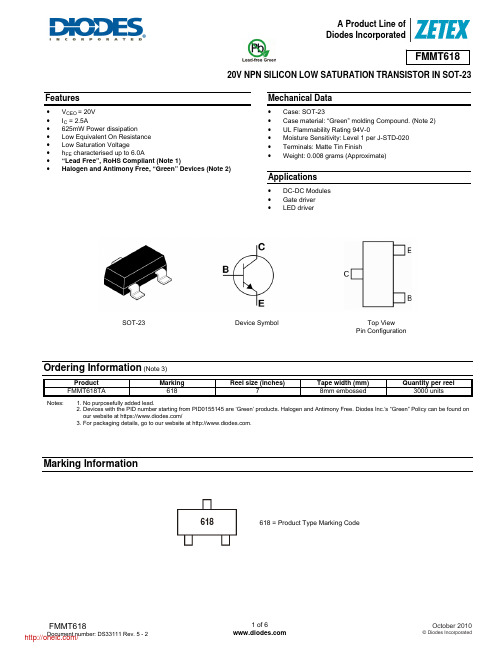
A Product Line ofDiodes Incorporated20V NPN SILICON LOW SATURATION TRANSISTOR IN SOT-23Features• V CEO = 20V • I C = 2.5A • 625mW Power dissipation • Low Equivalent On Resistance • Low Saturation Voltage • h FE characterised up to 6.0A • “Lead Free”, RoHS Compliant (Note 1) • Halogen and Antimony Free, “Green” Devices (Note 2)Mechanical Data• Case: SOT-23• Case material: “Green” molding Compound. (Note 2) • UL Flammability Rating 94V-0 • Moisture Sensitivity: Level 1 per J-STD-020 • Terminals: Matte Tin Finish • Weight: 0.008 grams (Approximate)Applications• DC-DC Modules • Gate driver • LED driverOrdering Information (Note 3)Product Marking Reel size (inches)Tape width (mm) Quantity per reelFMMT618TA618 7 8mm embossed 3000 unitsNotes:1. No purposefully added lead.2. Devices with the PID number starting from PID0155145 are ‘Green’ products. Halogen and Antimony Free. Diodes Inc.‘s “Green” Policy can be found on our website at https:///3. For packaging details, go to our website at .Marking Information618 = Product Type Marking CodeSOT-23Device SymbolTop View Pin Configuration618Maximum Ratings@T A = 25°C unless otherwise specifiedUnit Characteristic SymbolValueCollector-Base Voltage V CBO20 VCollector-Emitter Voltage V CEO20 VEmitter-Base Voltage V EBO 5 V Continuous Collector Current I C 2.5 APeak Pulse Current (Note 4) I CM 6 ABase Current I B500 mA Thermal CharacteristicsUnit Characteristic SymbolValuePower Dissipation at T A = 25°C (Note 5) P D625 mWThermal Resistance, Junction to Ambient Air (Note 4) @ T A = 25°C RθJA200 °C/WOperating and Storage Temperature Range T J, T STG-55 to +150 °CNotes: 4. Measured under pulsed conditions. Pulse width = 300µs. Duty cycle ≤ 2%.5. For a device surface mounted on 25mm X 25mm FR4 PCB with high coverage of single sided 1 oz copper, in still air conditions.Thermal Characteristics and Derating informationElectrical Characteristics @T A = 25°C unless otherwise specifiedCharacteristic Symbol Min Typ Max Unit Test ConditionCollector-Base Breakdown Voltage V (BR)CBO 20 100 - V I C = 100µA Collector-Emitter Breakdown Voltage (Note 6) V (BR)CEO 20 27 - V I C = 10mA Emitter-Base Breakdown Voltage V (BR)EBO 5 8.3 - V I E = 100µA Collector Cut-off Current I CBO - - 100 nA V CB =16V Emitter Cut-off Current I EBO - - 100 nA V EB = 4V Collector Emitter Cut-off Current I CES - - 100 nA V CES =16VStatic Forward Current Transfer Ratio (Note 6) h FE 200 300 200 100 400 450 360 180 --- - - I C = 10mA, V CE = 2V I C = 200mA, V CE = 2V I C = 2A, V CE = 2VI C = 6A, V CE = 2VCollector-Emitter Saturation Voltage (Note 6) V CE(sat)-- - 8 70 130 15 150 200 mV I C =0.1A, I B = 10mA I C =1A, I B = 10mA I C =2.5A, I B = 50mA Base-Emitter Saturation Voltage (Note 6) V BE(sat)- 0.89 1.0 V I C =2.5A, I B = 50mA Base-Emitter Saturation Voltage (Note 6) V BE(on)- 0.79 1.0 V I C =2.5A, V CE = 2V Transition Frequency f T100 140 - MHz I C = 50mA, V CE = 10V,f=100MHzCollector Output Capacitance C obo - 23 30 pF V CB = 10V, f=1MHz Turn-On Time t (on) - 170 - ns V CC = 10V, I C = 1A,I B1 = -I B2 = 10mA Turn-Off Time t (off)- 400 - ns Notes:6. Measured under pulsed conditions. Pulse width = 300µs. Duty cycle ≤ 2%Typical CharacteristicsA Product Line ofDiodes IncorporatedPackage Outline Dimensionsb 3Dim. Millimeters InchesDim. MillimetersInchesMin. Max. Min. Max.Min. Max. Min. Max. A-1.12-0.044e11.90 NOM0.075 NOMA1 0.01 0.10 0.0004 0.004 E 2.10 2.64 0.083 0.104 b 0.30 0.50 0.012 0.020 E1 1.20 1.40 0.047 0.055 c 0.085 0.20 0.003 0.008 L0.25 0.60 0.0098 0.0236D 2.80 3.04 0.110 0.120 L1 0.45 0.62 0.018 0.024 e 0.95 NOM 0.037 NOM - - - - -Note: Controlling dimensions are in millimeters. Approximate dimensions are provided in inchesSuggested Pad LayoutA Product Line ofDiodes IncorporatedIMPORTANT NOTICEDIODES INCORPORATED MAKES NO WARRANTY OF ANY KIND, EXPRESS OR IMPLIED, WITH REGARDS TO THIS DOCUMENT, INCLUDING, BUT NOT LIMITED TO, THE IMPLIED WARRANTIES OF MERCHANTABILITY AND FITNESS FOR A PARTICULAR PURPOSE (AND THEIR EQUIVALENTS UNDER THE LAWS OF ANY JURISDICTION).Diodes Incorporated and its subsidiaries reserve the right to make modifications, enhancements, improvements, corrections or other changes without further notice to this document and any product described herein. Diodes Incorporated does not assume any liability arising out of the application or use of this document or any product described herein; neither does Diodes Incorporated convey any license under its patent or trademark rights, nor the rights of others. Any Customer or user of this document or products described herein in such applications shall assume all risks of such use and will agree to hold Diodes Incorporated and all the companies whose products are represented on Diodes Incorporated website, harmless against all damages.Diodes Incorporated does not warrant or accept any liability whatsoever in respect of any products purchased through unauthorized sales channel. Should Customers purchase or use Diodes Incorporated products for any unintended or unauthorized application, Customers shall indemnify and hold Diodes Incorporated and its representatives harmless against all claims, damages, expenses, and attorney fees arising out of, directly or indirectly, any claim of personal injury or death associated with such unintended or unauthorized application.Products described herein may be covered by one or more United States, international or foreign patents pending. Product names and markings noted herein may also be covered by one or more United States, international or foreign trademarks.LIFE SUPPORTDiodes Incorporated products are specifically not authorized for use as critical components in life support devices or systems without the express written approval of the Chief Executive Officer of Diodes Incorporated. As used herein:A. Life support devices or systems are devices or systems which: 1. are intended to implant into the body, or2. support or sustain life and whose failure to perform when properly used in accordance with instructions for use provided in thelabeling can be reasonably expected to result in significant injury to the user.B. A critical component is any component in a life support device or system whose failure to perform can be reasonably expected to cause the failure of the life support device or to affect its safety or effectiveness.Customers represent that they have all necessary expertise in the safety and regulatory ramifications of their life support devices or systems, and acknowledge and agree that they are solely responsible for all legal, regulatory and safety-related requirements concerning their products and any use of Diodes Incorporated products in such safety-critical, life support devices or systems, notwithstanding any devices- or systems-related information or support that may be provided by Diodes Incorporated. Further, Customers must fully indemnify Diodes Incorporated and its representatives against any damages arising out of the use of Diodes Incorporated products in such safety-critical, life support devices or systems.Copyright © 2010, Diodes Incorporated分销商库存信息:DIODESFMMT618TA FMMT618TC。

The MT8510A Service Tester is designed for failure diagnosis of mobile terminal conforming to the 3rd-generation communica-tion system, W-CDMA.Along with the popularization of mobile equipment, especially mobile phones in recent years, the mobile terminal is becoming more and more close to the users’life.This trend enhances the importance of after-sales service that bears the reliability of mobile terminal day by day.The MT8510A features simple operability without requiring any expertise on mobile terminal, test contents conforming to the envi-ronment where mobile terminal is used and network administration support by remote control.It is useful at after service points of mobile terminal, ranging from sales points of mobile phones (service points) to repair/adjustment points (service centers).Simple operabilityTesting starts only by selecting the mobile equipment model on LCD of the mainframe and then pressing a START button.After the test, evaluation results are immediately displayed on LCD and LED.The results are printed out when the setting ofbuilt-in printer is ON.Power switchBuilt-in printer:For test result display Setup buttons for built-in printer START button:For test start STOP button:For test endUP/DOWN button:For selection of settingsENTER button:For fixation of settings Earphone jack:For voice testLCD :Parameter selection and result display LED (red):Lights during failure evaluation LED (green):Lights during normal evaluation LED (orange):Lights during test123456789101112Upper:MA8120A (Sold separately)Lower:MT8510ATest contentsFor accurate decision of defective mobile terminal as “defective”,it is necessary to perform measurements in the environment similar to the field where mobile equipment is actually used.•Protocol testThe MT8510A performs call connection/disconnection with mobile terminal by functioning as a base station simulator and makes the decision of [process succeeded/failed].The MT8510A is capable of performing evaluations to indi-vidual call process of [location registration], [origination],[termination], [disconnection from mobile terminal] and [dis-connection from network].•Performance testMobile equipment and base stations are combined by air con-nection.Accordingly, tests should be conducted under the sim-ilar environment.Comprehensive evaluation including mobile terminal’s antenna is achieved by setting the mobile terminal in shield box with a built-in wide band antenna (MA8120A, separately sold) and conducting performance test under air connection between mobile terminal and MT8510A.It is also possible to perform tests by connecting mobile equipment and MT8510A with a cable.The MT8510A performs each test of max.output power,closed-loop power control, modulation accuracy and frequency error as failure evaluation of mobile equipment’s transmitter,and Bit Error Rate (BER) test in loop-back status as failure evaluation of mobile terminal’s receiver.In each performance test, test item selection and evaluation threshold setting are created/saved in file format (test parame-ter) with remote control software of standard attachment.Also,Anritsu is able to create the test parameters.Please contact Anritsu sales representative for detail.Network support by remote controlNetwork administration of MT8510As, allocated in each ser-vice point and service center, is convenient for efficient operation.The installation of remote control software (standard attach-ment) in a PC enables remote controlling of testexecution/stop, MT8510A setups such as IP address setting and downloading of MT8510A mainframe firmware and test parameters.MA8120AMT8510ASpecificationsFrequency Transmitter:2110 to 2170 MHz Receiver:1920 to 1980 MHz, Setting resolution:200 kHz I/O connector N type, Impedance:50 Ω, VSWR:≤1.50Frequency:19.2 MHzReference Starting characteristics:≤±5 x 10⁻⁸(after 5 min.warm-up, referenced to frequency after 24 hour warm-up)oscillatorAging rate:≤±1 x 10⁻⁸/day, ≤±8 x 10⁻⁸/year (referenced to frequency after 24 hour warm-up)TotalTemperature characteristics:≤±3 x 10⁻⁸(0˚ to +70 ˚C, referenced to frequency at 25 ˚C)Reference signal output:BNC type, Impedance 50 ΩOutput level Level range:–110 to –45 dBm, Resolution:0.1 dB Accuracy:±1.5 dB (–110 to –45 dBm)Input level Level range:–30 to +27 dBmMeasurement accuracy ∗:±1.0 dB (0 to +27 dBm), ±1.2 dB (–20 to 0 dBm), ±1.5 dB (–30 to –20 dBm)Protocol testLocation registration, origination, termination, disconnection from mobile terminal, disconnection from network Test itemPerformance test Max.output power, closed-loop power control, frequency error, modulation accuracy BER test by loop back Communications testVoice Communications test by tester loop back (echo back)DisplayLCD:16 x 2 characters, LED:Testing (orange), Pass (green), Fail (red) External interface Ethernet 10BASE-T/100BASE-TXPowerInput voltage:AC 100 to 120 V/200 to 250 V , automatic selection, 47.5 to 63 Hz Dimensions and mass320 (W) x 134.5 (H) x 350 (D) mm, ≤6 k gOperating temperature range Operating:0˚ to +50 ˚C, Storage:–20 to +60 ˚CEMC EN61326:1997/A1:1998 (Class A), EN61000-3-2:1995/A2:1998 (Class A), EN61326:1997/A1:1998 (Annex A)LVD EN61010-1:1993/A2:1995 (Installation Category II, Pollution degree 2)Other Self-diagnostic function∗: 25 ±5 ˚COrdering informationPlease specify model/order number, name and quantity when ordering.∗1 This is essential software for call processing with W-CDMA mobile terminal.∗2 Recommended Remote PC spec.Interface :10BASE-T/100BASE-TXOS:Windows98/ME/2000, Windows NT4.0, CPU:≤400 MHz, Memory:≤64 MB, HDD:≤25 MBModel/Order Main frame MT8510AService TesterSoftwareMX851020AW-CDMA Call Processing Software ∗1Standard accessories Power, 2.6 m: 1 pc F0023Fuse, 3.15 A:1 pc J1109B 10BASE-T cross cable, 3 m: 1 pcZ0618Printer sheet, 5 roll:1 set W2094AE MT8510A operation manual (CD-ROM): 1 copy W2095AE MT8510A quick start manual: 1 copyMX851000A W-CDMA SoftwareMX851010AMT8510A Remote Control Software ∗2Application partsP0019TEST USIM 001J1110B 10BASE-T straight cable, 5 m J1158A UE I/F cable, 1.5 mJ1159A Coaxial cord, 1.5 m BA-A858Adaptor (N-P · SMA-J)ANRITSU CORPORATION5-10-27, Minamiazabu, Minato-ku, Tokyo 106-8570, Japan Phone:+81-3-3446-1111Telex:J34372Fax:+81-3-3442-0235•U.S.A.ANRITSU COMPANYNorth American Region Headquarters1155 East Collins Blvd., Richardson, TX 75081, U.S.A.Toll Free:1-800-ANRITSU (267-4878)Phone:+1-972-644-1777Fax:+1-972-671-1877•CanadaANRITSU ELECTRONICS LTD.700 Silver Seven Road, Suite 120, Kanata, ON K2V 1C3, CanadaPhone:+1-613-591-2003 Fax:+1-613-591-1006•BrasilANRITSU ELETRÔNICA LTDA.Praia de Botafogo 440, Sala 2401 CEP 22250-040, Rio de Janeiro, RJ, Brasil Phone:+55-21-5276922 Fax:+55-21-537-1456•U.K.ANRITSU LTD.200 Capability Green, Luton, Bedfordshire LU1 3LU, U.K.Phone:+44-1582-433200 Fax:+44-1582-731303•Germany ANRITSU GmbHGrafenberger Allee 54-56, 40237 Düsseldorf, Germany Phone:+49-211-96855-0 Fax:+49-211-96855-55•FranceANRITSU S.A.9, Avenue du Québec Z.A.de Courtabœuf 91951 Les Ulis Cedex, FrancePhone:+33-1-60-92-15-50Fax:+33-1-64-46-10-65•ItalyANRITSU S.p.A.Via Elio Vittorini, 129, 00144 Roma EUR, Italy Phone:+39-06-509-9711 Fax:+39-06-502-24-25•SwedenANRITSU ABBotvid Center, Fittja Backe 1-3 145 84 Stockholm,SwedenPhone:+46-853470700 Fax:+46-853470730•SpainANRITSU ELECTRÓNICA,S.A.Europa Empresarial Edificio Londres, Planta 1, Oficina 6 C/ Playa de Liencres, 2 28230 Las Rozas.Madrid,SpainPhone:+34-91-6404460Fax:+34-91-6404461•SingaporeANRITSU PTE LTD.10, Hoe Chiang Road #07-01/02, Keppel Towers,Singapore 089315Phone:+65-6282-2400 Fax:+65-6282-2533•Hong KongANRITSU COMPANY LTD.Suite 719, 7/F ., Chinachem Golden Plaza, 77 Mody Road, Tsimshatsui East, Kowloon, Hong Kong, China Phone:+852-2301-4980Fax:+852-2301-3545•KoreaANRITSU CORPORATION14F Hyun Juk Bldg.832-41, Yeoksam-dong, Kangnam-ku, Seoul, Korea Phone:+82-2-553-6603Fax:+82-2-553-6604˜5•AustraliaANRITSU PTY LTD.Unit 3/170 Forster Road Mt.Waverley, Victoria, 3149,AustraliaPhone:+61-3-9558-8177Fax:+61-3-9558-8255•TaiwanANRITSU COMPANY INC.7F , No.316, Sec.1, NeiHu Rd., Taipei, Taiwan Phone:+886-2-8751-1816Fax:+886-2-8751-1817Specifications are subject to change without notice.030123。
MTK手机芯片详细总纲前联发科技已开发出MT6205、MT6217、MT6218、MT6219、MT6226、MT6227、MT6228等系列平台,其中MT6205、MT6217、MT6218、MT6219、MT6226、MT6227、MT6228均为基带芯片,所有芯片均采用ARM7的核。
MT6305、MT6305B为电源管理芯片。
MT6129为RF芯片RF3146(7×7mm)、RF3146D(双频)、RF3166(6×6mm)为RFMD的PA。
MT6205为最早的方案,只有GSM的基本功能,不支持GPRS、WAP、MP3等功能。
(2003年MP)MT6218为在MT6205基础上增加GPRS、WAP、MP3功能。
MT6217为MT6218的cost down方案,与MT6128 PIN TO PIN,只是软件不同而已,另外MT6217支持16bit数据。
(2004年MP)MT6219为MT6218上增加内置AIT的1.3M camera处理IC,增加MP4功能。
8bit数据。
(2005年MP)MT6226为MT6219 cost 升级产品,内置0.3M 摄相处理IC,支持GPRS、WAP、MP3、MP4等,内部配置比MT6219优化及改善,比如配蓝牙是可用很便宜的芯片CSR的BC03模块USD3即可支持数据传输(如听立体声MP3等)功能。
MT6226M为MT6226高配置设计,内置的是1.3M摄像处理IC。
(2006年MP)MT6227与MT6226功能基本一样,PIN TO PIN,只是内置的是2.0M 摄像处理IC。
(2006年MP)MT6228比MT6227增加TV OUT功能,内置3.0M 摄像处理IC,支持支持GPRS、WAP、MP3、MP4。
(2006年MP)从MT6226后软件均可支持网络摄像头功能,也就是说你的机子可以用于QQ视频。
MTK芯片工作简解现在最长见的MTK手机芯片组合多是MT6128BT CPU(MT6219CPU)、MT6035电源IC和MT6129射频IC组合,以下是对MT芯片的简单讲解。
1Features•Programmable m-Law/A-Law CODEC and Filters•Programmable CCITT (G.711)/sign-magnitude coding•Programmable transmit, receive and side-tone gains•Digital DTMF and single tone generation •Fully differential interface to handset transducers•Auxiliary analog interface•Interface to ST-BUS/SSI (compatible with GCI)•Serial microport control•Single 5 volt supply, low power operation •Anti-howl circuit for group listening speakerphone applicationsApplications•Digital telephone sets •Wireless telephones•Local area communications stationsDescriptionThe MT9196 Integrated Digital Phone Circuit (IDPC) is designed for use in digital phone products. The device incorporates a built-in Filter/Codec, digital gain pads,DTMF generator and tone ringer. Complete telephony interfaces are provided for connecting to handset and speakerphone transducers. Internal register access is provided through a serial microport compatible with various industry standard micro-controllers.The device is fabricated in Zarlink's ISO 2-CMOS technology ensuring low power consumption and high reliability.January 2006Ordering InformationMT9196AP 28 Pin PLCC Tubes MT9196AE 28 Pin PDIP Tubes MT9196AS 28 Pin SOIC Tubes MT9196ASR 28 Pin SOIC Tape & Reel MT9196APR 28 Pin PLCC Tape & Reel MT9196AE128 Pin PDIP*Tubes MT9196APR128 Pin PLCC*Tape & Reel MT9196AP128 Pin PLCC*Tubes MT9196AS128 Pin SOIC*Tubes MT9196ASR128 Pin SOIC*Tape & Reel*Pb Free Matte Tin-40°C to +85°CISO 2-CMOSMT9196Integrated Digital Phone Circuit (IDPC)Data SheetFigure 1 - Functional Block DiagramMT9196Data SheetFigure 2 - Pin ConnectionsPin Description Pin #Name Description1M-Inverting Microphone (Input). Inverting input to microphone amplifier from the handset microphone.2M+Non-Inverting Microphone (Input). Non-inverting input to microphone amplifier from the handset microphone.3V Bias Bias Voltage (Output). (V DD /2) volts is available at this pin for biasing external amplifiers. Connect 0.1 µF capacitor to V SSA .4V Ref Reference voltage for codec (Output). Nominally [(V DD /2)-1.5] volts. Used internally. Connect 0.1 µF capacitor to V SSA .5PWRST Power-up Reset (Input). CMOS compatible input with Schmitt Trigger (active low).6IC Internal Connection. Tie externally to V SS for normal operation.7V SSD Digital Ground. Nominally 0 volts.8CS Chip Select (Input). This input signal is used to select the device for microport data transfers. Active low. TTL level compatible.9SCLK Serial Port Synchronous Clock (Input). Data clock for microport. TTL level compatible.10DATA1Bidirectional Serial Data. Port for microprocessor serial data transfer. In Motorola/National mode of operation, this pin becomes the data transmit pin only and data receive is performed on the DATA2 pin. TTL level compatible input levels.11DATA2Serial Data Receive. In Motorola/National mode of operation, this pin is used for data receive to the IDPC. In Intel mode, serial data transmit and receive are performed on the DATA1 pin and DATA2 is disconnected. Input level TTL compatible.12WDWatchdog (Output). Watchdog timer output. Active high.13IRQInterrupt Request (Open Drain Output). Low true interrupt output to microcontroller.AUXin MIC+VDD HSPKR-HSPKR+SPKR-SPKR+VSS SPKR AUXout VSSA STB/F0i CLOCKin XSTAL2DinM-M+VBias VRef PWRSTIC VSSD CS SCLK DATA1DATA2IRQ WD Dout 28 PIN PLCC 28 PIN SOIC/PDIP165432789101123192021222425262728M -M +V B i a sV R e f PWRSTIC VSSD CS SCLK DATA1DATA2VDDHSPKR-HSPKR+SPKR-SPKR+VSS SPKR AUXout A U X i nM I C +V S S A 12131415161718I R Q D i n S T B /F 0i C L O C K i n X S T A L 2D o u t W D 17181920282726252423222116151234567891011121314MT9196Data Sheet Pin Description (continued)Pin #Name Description14D out Data Output. A tri-state digital output for 8 bit wide channel data being sent to the Layer 1 device. Data is shifted out via this pin concurrent with the rising edge of BCL during thetimeslot defined by STB, or according to standard ST-BUS timing.15D in Data Input. A digital input for 8 bit wide channel data received from the Layer 1 device. Data is sampled on the falling edge of BCL during the timeslot defined by STB, or according tostandard ST-BUS timing. Input level is CMOS compatible.16STB/F0i Data Strobe/Frame Pulse (Input). For SSI mode this input determines the 8 bit timeslot used by the device for both transmit and receive data. This active high signal has a repetitionrate of 8 kHz. Standard frame pulse definitions apply in ST-BUS mode. CMOS levelcompatible input.17CLOCKin Clock Input. The clock provided to this input is used by the internal phone functions. In ST-BUS mode this is the C4i input. In SSI synchronous mode, this is the Bit Clock input. In SSI-asynchronous mode this is an asynchronous 4 MHz Master Clock input.18XSTL2Crystal Input (4.096 MHz). Used in conjunction with the CLOCKin pin to provide the master clock signal via external crystal.19V DD Positive Power Supply (Input). Nominally 5 volts.20HSPKR-Inverting Handset Speaker (Output). Output to the handset speaker (balanced).21HSPKR+Non-Inverting Handset Speaker (Output). Output to the handset speaker (balanced).22SPKR-Inverting Speaker (Output). Output to the speakerphone speaker (balanced).23SPKR+Non-Inverting Speaker (Output). Output to the speakerphone speaker (balanced).24V SS SPKR Power Supply Rail for Speaker Driver. Nominally 0 Volts.25AUX out Auxiliary Port (Output). Access point to the D/A (analog) signals of the receive path as well as to the various analog inputs.26AUX in Auxiliary Port (Input). An analog signal may be fed to the filter/codec transmit section and various loopback paths via this pin. No external anti-aliasing is required.27MIC+Non-inverting on-hook answer back Microphone (Input). Microphone amplifier non-inverting input pin.28V SSA Analog Ground (Input). Nominally 0 V.OverviewThe functional block diagram of Figure 1 depicts the main operations performed by the MT9196 IDPC. Each of these functional blocks will be described individually in the sections to follow. This overview will describe some of the end-user features which may be implemented as a direct result of the level of integration found within the IDPC. The main feature required of a digital telephone is to convert the digital Pulse Code Modulated (PCM) information, being received by the telephone set, into an analog electrical signal. This signal is then applied to an appropriate audio transducer such that the information is finally converted into intelligible acoustic energy. The same is true of the reverse direction where acoustic energy is converted first into an electrical analog and then digitized (into PCM) before being transmitted from the set. Along the way if the signals can be manipulated, either in the analog or the digital domains, other features such as gain control and signal generation may be added. Finally, most electro-acoustic transducers (loudspeakers) require a large amount of power if they are to develop an acoustic signal. The inclusion of audio amplifiers to provide this power is required.MT9196Data Sheet The IDPC features complete Analog/Digital and Digital/Analog conversion of audio signals (Filter/CODEC) and an analog interface to electro-acoustic devices (Transducer Interface). Full programmability of the receive path and side-tone gains is available to set comfortable listening levels for the user. Transmit path gain control is available for setting nominal transmit levels into the network. A digital, anti-feedback circuit permits both the handset microphone and the speaker-phone speaker to be enabled at the same time for group listening applications. This anti-feedback circuit limits the total loop gain there by preventing a singing condition from developing.Signalling in digital telephone systems, behind the PBX or standard ISDN applications, is handled on the D-channel and generally does not require DTMF tones. Locally generated tones, in the set, however, can be used to provided “comfort tones” or “key confirmation” to the user, similar to the familiar DTMF tones generated by conventional phones during initial call set-up. Also, as the network slowly evolves from the dial pulse/DTMF methods to the D-Channel protocols it is essential that the older methods be available for backward compatibility. As an example, once a call has been established (i.e., from your office to your home) using the D-Channel signalling protocol it may be necessary to use in-band DTMF signalling to manipulate your personal answering machine in order to retrieve messages. Thus the locally generated tones must be of network quality. The IDPC can generate the required tone pairs as well as single tones to accommodate any in-band signalling requirement.Each of the programmable parameters within the functional blocks is accessed through a serial microcontroller port compatible with Intel MCS-51®, Motorola SPI® and National Semiconductor Microwire® specifications. Functional DescriptionIn this section each of the functional blocks within IDPC is described along with all of the associated control/status bits. Each time a control/status bit(s) is described it is followed by the address register where it will be found. The reader is referred to the section titled 'Register Summary' for a complete listing of all address registers, the control/status bits associated with each register and a definition of the function of each control/status bit. The Register Summary is useful for future reference of control/status bits without the need to locate them in the text of the functional descriptions.Filter/CODECThe Filter/CODEC block implements conversion of the analog 3.3 kHz speech signals to/from the digital domain compatible with 64 kb/s PCM B-Channels. Selection of companding curves and digital code assignment are register programmable. These are CCITT G.711 A-law or µ-Law, with true-sign/ Alternate Digit Inversion or true-sign/Inverted Magnitude coding, respectively. Optionally, sign- magnitude coding may also be selected for proprietary applications.The Filter/CODEC block also implements transmit and receive audio path gains in the analog domain. These gains are in addition to the digital gain pad section and provide an overall path gain resolution of 1.0dB. A programmable gain, voice side-tone path is also included to provide proportional transmit speech feedback to the handset receiver. Figure 3 depicts the nominal half-channel and side-tone gains for the IDPC.On PWRST (pin 5) the Filter/CODEC defaults such that the side-tone path, dial tone filter and 400 Hz transmit filter are off, all programmable gains are set to 0dB and CCITT µ-Law is selected. Further, the Filter/CODEC is powered down due to the control bits of the Path Control Registers (addresses 12h and 13h) being reset.The internal architecture is fully differential to provide the best possible noise rejection as well as to allow a wide dynamic range from a single 5 volt supply design. This fully differential architecture is continued into the Transducer Interface section to provide full chip realization of these capabilities for the handset and loudspeaker functions.A reference voltage (V Ref), for the conversion requirements of the CODEC section, and a bias voltage (V Bias), for biasing the internal analog sections, are both generated on-chip. V Bias is also brought to an external pin so that it may be used for biasing external gain plan setting amplifiers. A 0.1 µF capacitor must be connected from V Bias to analog ground at all times. Likewise, although V Ref may only be used internally, a 0.1 µF capacitor from the V Ref pin to ground is required at all times. The analog ground reference point for these two capacitors must be physically the same point. To facilitate this the V Ref and V Bias pins are situated on adjacent pins.MT9196Data Sheet The transmit filter is designed to meet CCITT G.714 specifications. The nominal gain for this filter path is 0 dB (gain control = 0 dB). Gain control allows the output signal to be increased up to 7 dB. An anti-aliasing filter is included. This is a second order lowpass implementation with a corner frequency at 25 kHz. Attenuation is better than 32 dB at 256 kHz and less than 0.01 dB within the passband.An optional 400Hz high-pass function may be included into the transmit path by enabling the Tfhp bit in the Control Register 1 (address 0Eh). This option allows the reduction of transmitted background noise such as motor and fan noise.Figure 3 - Audio Gain PartitioningThe receive filter is designed to meet CCITT G.714 specifications. The nominal gain for this filter path is 0 dB (gain control = 0dB). Gain control allows the output signal to be attenuated up to 7 dB. Filter response is peaked to compensate for the sinx/x attenuation caused by the 8 kHz sampling rate.The Rx filter function can be altered by enabling the Dial EN control bit in Control Register 1 (address 0Eh). This causes another low-pass function to be added with a 3 dB point at 1200 Hz. This function is intended to improve the sound quality of digitally generated dial tone received as PCM.Side-tone is derived from the Tx filter before the LP/HP filter section and is not subject to the gain control of the Tx filter section. Side-tone is summed into the receive handset transducer driver path after the Rx filter gain controlMT9196Data Sheetsection so that Rx gain adjustment will not affect side-tone levels. The side-tone path may be enabled/disabled with the Voice sidetone bit located in the Receive Path Control Register (address 13h).Transmit and receive filter gains are controlled by the TxFG 0-TxFG 2 and RxFG 0-RxFG 2 control bits, respectively.These are located in the FCODEC Control Register 1 (address 0Ah). Transmit filter gain is adjustable from 0 dB to +7 dB and receive filter gain from 0 dB to -7 dB, both in 1 dB increments.Side-tone filter gain is controlled by the STG 0-STG 2 control bits located in the FCODEC Control Register 2(address 0Bh). Side-tone gain is adjustable from -9.96 dB to +9.96 dB in 3.32 dB increments.Companding law selection for the Filter/CODEC is provided by the A/µ companding control bit while the coding scheme is controlled by the sign-mag/CCITT control bit. Both of these reside in Control Register 2 (address 0Fh).Table 1 illustrates these choices.Table 1The Filter/CODEC autonull circuit ensures that transmit PCM will contain no more than ±1 bit of offset due to internal circuitry.Digital Gain and Tone GenerationThe Digital gain and Tone generator block is located, functionally, between the serial FDI port and the Filter/CODEC block. Its main function is to provide digital gain control of the transmit and receive audio signals and to generate digital patterns for DTMF and tone ringer signals.Gain ControlGain control is performed on linear code for both the receive and the transmit PCM. Gain control is set via the Digital Gain Control Register at address 19h. Gain, in 3.0 dB increments, is available within a range of +21.0 dB to -24 dB.DTMF GeneratorThe digital DTMF circuit generates a dual sine-wave pattern which may be routed into the receive path as comfort tones or into the transmit path as network signalling. In both cases the digitally generated signal will undergo gain adjustment as programmed into the transmit and receive gain control registers. Gain control is assigned automatically as functions are selected via the transmit and receive path control registers.The composite signal output level in the transmit direction is -4 dBm0 (µ-Law) and -10 dBm0 (A-law) with programmable gains at zero dB. Pre-twist of 2.0 dB is incorporated into the composite signal resulting in a low tone output level of -8.12 dBm0 and a high group level of -6.12dBm0 (for µ-Law, 6 dB lower for A-Law). Note that these levels will be influenced by the Anti-Howling circuit when it is enabled (see Anti-Howling section for more details).DTMF side-tone levels are set to -28 dBm0 from the generator circuit. Other receive path gains must be included when calculating the analog output signal levels. Adjustments to these levels may be made by altering the settings of the Gain Control register (address 19h).CodeSign/MagnitudeCCITT (G.711)µ-LawA-Law+ Full Scale 1111 11111000 00001010 1010+ Zero 1000 00001111 11111101 0101-Zero (quiet code)0000 00000111 11110101 0101- Full Scale0111 11110000 00000010 1010MT9196Data SheetThe frequency of the low group tone is programmed by writing an 8-bit coefficient into the Low Tone Coefficient Register (address 1Ah) while the high group tone frequency uses the 8-bit coefficient programmed into the High Tone Coefficient Register (address 1Bh). Both coefficients are determined by the following equation:Frequency (in Hz) = 7.8125 x COEFFWhere COEFF is an integer between 0 and 255. Frequency resolution is 7.8125 Hz in the range 0 to 1992 Hz.Low and high tones are enabled individually via the LoEn and HiEN control bits (DTMF/Ringer Control Register,address 18h). This not only provides control over dual tone generation but also allows single tone generation using either of the enable bits and its associated coefficient register.After programming and enabling the tone generators as described, selection of transmit and/or receive path destinations are carried out via the Path Control Registers (see Path Control section). In addition receive sidetone DTMF must be selected via the DTMF StEN bit (DTMF/Tone ringer Register, address 18h) so that it replaces the received PCM in the Rx Filter path.DTMF Signal to distortion:The sum of harmonic and noise power in the frequency band from 50 Hz to 3500 Hz is typically more than 30 dB below the power in the tone pair. All individual harmonics are typically more than 40 dB below the level of the low group tone.Table 2 gives the standard DTMF frequencies, the coefficient required to generate the closest frequency, the actual frequency generated and the percent deviation of the generated tone from the nominal.Tone RingerA dual frequency squarewave ringing signal may be applied to the handsfree speaker driver to generate a call alerting signal. To enable this mode the Ring En bit (address 18h) must be set as well as the ringer function to the loudspeaker via the Receive Path Control Register (address 13h). Ring En is independent of the DTMF enable control bits (see Lo EN and Hi EN). Since both functions use the same coefficient registers they are not usually enabled simultaneously.The digital tone generator uses the values programmed into the low and high Tone Coefficient Registers (addresses 1Ah and 1Bh) to generate two different squarewave frequencies. Both coefficients are determined by the following equation:COEFF = [32000/Frequency (Hz)] - 1where COEFF is an integer between 1 and 255. This produces frequencies between 125 - 16000 Hz with a non-linear resolution.The ringer program switches between these two frequencies at a 5 Hz or 10 Hz rate as selected by the WR bit in the DTMF/Tone ringer register (address 18h).Frequency(Hz)COEFF Actual Frequency %Deviation 69759h 695.3-.20%77063h 773.4+.40%8526Dh 851.6-.05%94179h 945.3+.46%12099Bh 1210.9+.20%1336ABh 1335.9.00%1477BDh 1476.6-.03%1633D1h1632.8-.01%Table 2 - DTMF FrequenciesMT9196Data SheetAnti-HowlIDPC includes an Anti-Howling circuit plus speaker gain control circuit to allow for group listening operation. Although this is the main function of the circuit there are additional modes in which it may be used as defined by the MS1 and MS0 control bits (address 1Ch).MS1MS0Operational Mode00Tx noise reduction (squelch)01Rx noise reduction (squelch)10switched loss group listening(anti-howling)11Tx/Rx switched lossThe circuit is enabled by setting the Anti-howl Enable bit (address 1Ch) and selecting the required operational mode (MS0 & MS1) as described.For all modes of operation the switching levels and inserted loss are programmed as follows.Switching decisions are made by comparing either the transmit or the receive signal level to threshold levels stored in the High Threshold Register (address 1Dh) and the Low Threshold Register (address 1Eh). Threshold data is encoded in PCM sign-magnitude format excluding the sign bit. For example; THh0 - THh3 encode the PCM step number while THh4 - THh6 encode the PCM chord number for the high threshold. Similarly for the THl0 - THl6 bits of the low threshold. The difference between the high and low threshold levels provides the circuit with hysteresis to prevent uncontrolled operation. The low level threshold must never be programmed to a value higher than the one stored in the high level threshold. If this occurs the circuit will become unstable.Loss is implemented, in the chosen path, by subtracting the value set by the Pad0 - Pad3 control bits from the appropriate gain value set by the RxG0 - RxG3 or TxG0 - TxG3 control bits (see Digital Gain Register, address 19h). The minimum digital gain is limited to -24 dB regardless of the mathematical result of this operation. The path without loss reverts to the gain value programmed into the Digital Gain Register.The magnitude of the switched loss defaults to 12 dB on power up but can be programmed to between 0 and 21 dB using the Pad0 - Pad2 control bits (address 1Ch).Pad2Pad1Pad0Attenuation (dB)000000130106011910012101151101811121Switched Loss for Group Listening (anti-howling)Group listening is defined as a normal handset conversation with received speech also directed to the loudspeaker for third party observation. In this mode, if the handset microphone is moved into close proximity of the loudspeaker a feedback path will occur resulting in a singing connection. To prevent this the anti-howling circuit introduces a switched loss into either the transmit or receive paths dependent upon the transmit path speech activity.Loss switching is determined by comparing the signal level in the transmit path with the high level threshold stored at address 1Dh. When the transmit signal level exceeds this threshold the programmed loss is switched from the transmit path to the receive path. Once switching has occurred the transmit signal level is then compared to a low level threshold stored at address 1Eh. When the transmit signal level falls below this threshold the programmed loss is switched from the received path back to the transmit path and comparison reverts back to the high threshold level.MT9196Data Sheet Since the received digital gain control is used to set the listening level of the received speech, for both handset receiver and loudspeaker, it is necessary to provide additional gain in the loudspeaker path so that its receive level can be controlled independently from the receiver output. The Gain0 to Gain3 control bits (address 0Bh) are used to boost the loudspeaker output to a comfortable listening level for the third parties in group listening. Generally the Gain3 bit should be set to logic 1 in this mode. This increases the gain programmed via the Gain0 - Gain2 bits by a factor of 8 dB. In group listening a speaker gain setting of 4 to 16 dB will be required to set a comfortable group listening level after the handset user has adjusted their listening level as required.Since the anti-howling circuit has dynamic control over the transmit and receive gain control registers, it is recommended that this function be turned off momentarily when DTMF tone generation is required. This will ensure that the proper transmit levels are attained.Transmit Noise Reduction (squelch)The transmit signal may be muted to eliminate transmission of excessive background noise.In this mode the signal level in the transmit path is compared with the high level threshold stored at address 1Dh. When the transmit signal level exceeds this threshold no loss is inserted into the transmit path. After exceeding the high level threshold the transmit signal level is then compared to a low level threshold stored at address 1Eh. When the transmit signal level falls below this threshold the transmit digital gain is reduced by the programmed amount (Pad0-2) and comparison reverts back to the high threshold level. The receive path gain is not altered by transmit noise reduction.Receive Noise Reduction (squelch)The receive signal may be muted to eliminate background noise resulting from a poor trunk connection.In this mode the signal level in the receive path is compared with the high level threshold stored at address 1Dh. When the receive signal level exceeds this threshold no loss is inserted into the receive path. After exceeding the high level threshold the receive signal level is then compared to a low level threshold stored at address 1Eh. When the receive signal level falls below this threshold the receive digital gain is reduced by the programmed amount (Pad2-0) and comparison reverts back to the high threshold level. The transmit path gain is not altered by receive noise reduction.Tx/Rx Switched LossIn this mode the programmed switched loss is inserted into either the transmit or receive path dependent only upon activity in the receive path. If receive path activity is above the programmed high level threshold then the switched loss is inserted into the transmit path. If receive path activity is below the programmed low level threshold then the switched loss is inserted into the receive path.This mode can be used to implement a loudspeaking function where the receive audio is routed to the SPKR± pins and transmit audio is sourced from the MIC+ pin. In this mode there is no algorithmic cancellation of echo so it is recommended that this switched loss program be used only in 4-wire systems (i.e., digital set to digital set). Transducer InterfacesFour standard telephony transducer interfaces plus an auxiliary I/O are provided by the IDPC. These are:•The handset microphone inputs (transmitter), pins M+/M- and the answerback microphone input MIC+. The nominal transmit path gain may be adjusted to either 6.0dB or 15.3dB. Control of this gain is provided by the TxINC control bit (Control register 2, address 0Fh). This gain adjustment is in addition to theprogrammable gain provided by the transmit filter and Digital Gain circuit.•The handset speaker outputs (receiver), pins HSPKR+/HSPKR-.Thisinternallycompensated, fully differential output driver is capable of driving the load shown in Figure 4. The nominal handset receive path gain may be adjusted to either -12.1 dB or -9.6 dB. Control of this gain is provided by the RxINC control bit (ControlMT9196Data Sheetregister 2, address 0Fh). This gain adjustment is in addition to the programmable gain provided by the receive filter and Digital Gain circuit.•The loudspeaker outputs, pins SPKR+/SPKR-. This internally compensated, fully differential output driver is capable of directly driving 6.5v p-p into a 40 ohm load.•The Auxiliary Port provides an analog I/O, pins AUXin and AUXout, for connection of external equipment to the CODEC path as well as allowing access to the speaker driver circuits.•AUXin is a single ended high impedance input (>10 Kohm). This is a self-biased input with a maximum input range of 2.5vp-p. Signals should be capacitor-coupled to this input.•AUXout is a buffered output capable of driving 40 Kohms//150 pF. Signals for this output are derived from the receive path or from the AUXin and transmit microphones.•Auxiliary port path gains are:Refer to the application diagrams of Figures 10 and 11 for typical connections to this analog I/O section.Figure 4 - Handset Speaker DriverMicroportThe serial microport, compatible with Intel MCS-51 (mode 0), Motorola SPI (CPOL=0,CPHA=0) and National Semiconductor Microwire specifications provides access to all IDPC internal read and write registers. This microport consists of a transmit/receive data pin (DATA1), a receive data pin (DATA2), a chip select pin (CS) and a synchronous data clock pin (SCLK).The microport dynamically senses the state of the serial clock each time chip select becomes active. The device then automatically adjusts its internal timing and pin configuration to conform to Intel or Motorola/National requirements. If SCLK is high during chip select activation then Intel mode 0 timing is assumed. The DATA1 pin is defined as a bi-directional (transmit/receive) serial port and DATA2 is internally disconnected. If SCLK is low during chip select activation then Motorola/National timing is assumed. Motorola processor mode CPOL=0, CPHA=0 must be used. DATA1 is defined as the data transmit pin while DATA2 becomes the data receive pin. Although the dualAUXin to Dout Din to AUXout AUXin to AUXout AUXin to HSPKR ±AUXin to SPKR ±11 dB 20.3 dB -12 dB -7.0 dB -1.1 dB 1.4 dB 5.0 dBTxINC=0TxINC=1RxINC=0RxINC=1HSPKR +HSPKR -75 Ω75 Ω150 ohm load (speaker)IDPC。
ATMEL - AT91SAM9G20-EK - AT91SAM9G20-EK EvaluationKitProduct Overview:The AT91SAM9G20-EK Evaluation Kit enables theevaluation of and code development for applicationsrunning on an AT91SAM9G20 device. This guidefocuses on the AT91SAM9G20-EK board as anevaluation platform. The board supports theAT91SAM9G20 in a 217-ball LFBGA RoHS-compliantPackage.Kit Contents:The AT91SAM9G20-EK package contains the following items:board∙ AnAT91SAM9G20-EK∙ A universal input AC/DC power supply with US and Europe plug adapter∙One A/B-type USB cable one serial RS232 cable∙One RJ45 crossed Ethernet cable∙One CD-ROM that allows the user to begin evaluating the AT91 ARM® Thumb® 32-bit microcontroller quickly∙One 3V Lithium batteryKey Features:∙64 Mbytes of SDRAM memory∙256 Mbytes of NAND Flash memory∙One Atmel® serial Data Flash®∙One Atmel TWI serial EEPROM∙One USB Device port interface∙Two USB Host port interfaces∙One DBGU serial communication port∙One complete MODEM serial communication port∙One additional serial communication port with RTS/CTS handshake control∙JTAG/ICE debug interface∙One PHY Ethernet 100-base TX with three status LEDs∙One on-board Audio DAC∙One Power LED and one general-purpose LED∙Two user-input push buttons∙One Wakeup-input push button∙One reset push button∙Two Data Flash SD/MMC card slots∙Four expansion connectors (PIOA, PIOB, PIOC, IMAGE SENSOR)∙One BGA-like EBI expansion footprint connector∙One Lithium Coin Cell Battery Retainer for 12 mm cell sizeOrdering Information:Products:Part Number Manufacturer Farnell P/N Newark P/NAT91SAM9G20-EK Atmel 1715470 15R0327 Associated Products:Part Number Manufacturer Description Farnell P/N Newark P/NAT91SAM-ICE Atmel ICE for AT91 ARM Cores1095464 23M5083AT91SAM9G20B-CU Atmel ARM9 Microcontroller 1715469 15R0328MAX3241ECAI+ Maxim RS-232 Transceiver9724940 68K4636LT1963AEQ-3.3#PBF Linear LDO Regulator1273626 57M7440TPS60500DGSR TI Step-down charge pump1412493 77C0634WM8731SEDS Wolfson Audio CODEC Driver 1776264 50M5333 Similar Products:Part Number Manufacturer Description SupportDeviceFarnellP/NNewarkP/NAT91SAM9261-EK AtmelEvaluation forAT91SAM926EJAT91SAM9261 1629538 02P6236AT91SAM9263-EK AtmelEvaluation forAT91SAM9263AT91SAM9263 1629539 02P6237AT91SAM9RL-EK AtmelEvaluation forAT91SAM9RL-EKAT91SAM9RL 1648589 11P0231AT91SAM9XE-EK AtmelEvaluation forAT91SAM9XE-EKAT91SAM9XE 1648590 11P0232Document List:Datasheets:Part Number Description SizeMAX3241E ±15kV ESD-Protected, Down to 10nA, 3.0V to 5.5V, up to 1Mbps,True RS-232 Transceivers298KBLT1963A Series 1.5A, Low Noise, fAST Transient Response LDO Regulators 278KBARM9TDMI ARM9TDMI Technical Reference Manual 920KBARM920T ARM920T Technical Reference Manual 2.11MBAT91SAM9G20B AT91SAM9G20B Microcontroller 12.1MBTPS60500 High efficiency, 250-mA, Step-down charge pump 510KBK9F2G08UXA K9F2G08UXA Flash Memory datasheet 999KBMT48LC64M4A2 MT48LC64M4A2 Synchronous DRAM 256MB 1.47MBWM8731 WM8731 Portable Internet Audio CODEC with Headphone Driver 762KBApplication Notes:File Name SizeAT91 Assembler Code Startup Sequence for C Code Applications Software 116KBAT91 Assembler Code Startup Sequence for C Code Applications Software Based on theAT91SAM7S64 Evaluate140KBAT91SAM9RL-EK Evaluation Board 968KBAT91SAM Internet Radio 425KB Connecting an Atmel ARM-based Serial Synchronous Controller to an I2S-compatible SerialBus114KBInterfacing a 4x4 Keyboard to an AT91 Microcontroller 898KBMigrating to an AT91SAM9G20-based System from an AT91SAM9260-based System 190KBPulse Width Modulation Generation Using the AT91 Timer and Counter 87KBUsing the ECC Controller on AT91SAM9260 and AT91SAM7SE Microcontrollers 774KBUsing the Serial Peripheral Interface with AT91SAMxx Devices 149KBUsing the Two-wire interface (TWI) in Master Mode on AT91SAM Microcontrollers 1.05MBInterfacing a Hard Disk Drive to an AT91RM9200 Microcontroller 112KBInterfacing a PC Card to an AT91RM9200-DK 184KBInterrupt Generation Using the AT91 Timer and Counter 112KBHardware & Software:File Name SizeAT91SAM9G20-EK Hardware Files 2.37MB Install AT91-ISP v1.13(Windows XP - v1.13 current release) 3.64MBSAM-BA_CDC(Windows Vista - v1.13 current release) 6.85MB。
MTK驱动调试相关总结 2010-12-14 Ver:1.11 SIM卡2 T卡3 FLASH4 按键KEY5 IO配置6 ADC配置7 EINT配置8 FM驱动9 BT驱动10 TOUCHSCEEN驱动11 LCM驱动12 Sensor驱动13 背光灯、按键灯、振动器、PWM14 跑马灯15 移动传感器、四方传感器16 MP4、3GP播放17 音量参数、EQ参数、音频功放开关18 SMS、电话本等容量设置19 耳机插入、拔出检查、耳机按键处理20 充电器或USB插入、拔出检查、识别21 RF 配置22参考文档附录默认系统平台为MT6253,code版本:09B.W10.12.MP。
版本变更记录:Andy 2010.12.10 Ver:1.0Andy 2010-12-14 Ver:1.11 SIM卡F910(MT6253)SIM卡插槽与系统SIM卡号映射关系drv\src\switchControl_al.c// andy 2010.05.31 SIM卡插槽映射 __DRV_DUAL_SIM_INVERSE__//kal_bool sim_physicalSlotChanged;#ifdef __DRV_DUAL_SIM_INVERSE__kal_bool sim_physicalSlotChanged = KAL_TRUE ;#elsekal_bool sim_physicalSlotChanged = KAL_FALSE;#endif定制支持的SIM电压:Customer_sim_voltage_support.c/* For customer define ME support voltage of SIM *//* For 1.8V Tech. ME use ME_18V_30V *//* For 3.0V ONLY ME use ME_30V_ONLY *//* For 1.8V ONLY ME use ME_18V_ONLY */#define SIM_VOLTAGE_SUPPORT ME_18V_30Vsim_env SIM_GetCurrentEnv(void){(SIM_VOLTAGE_SUPPORT);return}MT6253的“4.3 SIM Interface”,介绍了SIM卡接口的情况。
MT6189/MT6188 FM Radio Application
Introduction
Need to use inductor of Q>25; recommend Murata LQW15AN15NG .
Do not share with camera I 2C.
Reference circuit –MT6189
Recommend to keep this resistor if space is enough, in
case you want to do experiment on voltage source. FM_INL
R3
10k
C112p C9
100p VCC_FM
C10
47n
C32.2u
FM_ANT(earphone ground pin)
C8
100n
VCC_FM C6100n
R210k VCC_FM L2
15nH
R40 OHM C4220n
SCL
SDA
C7100n
L3
22uH
L1150nH VCC_FM U1
MT6189
123456789101112131415161718192021
22
23
24
25
26
27
28
293031
323335363738394034AFR NC NC NC NC GND VCCRF RFINP RFINN GNDRF N C N C V C
C V C O G N
D V
C O I N
D P I N D N C P
N C N C X
1/
X
I
N X2
NC NC NC NC MPX NC VCCST GNDST INT N C
N C L
E S C
L
N C B U S E V D
D
G N D D A F L S D A 32.768kHz
VCC_FM
FM_INR
C239p R151K AVDD C5
3.3n VCC_FM
MT6189 Reference Circuit
Application notes:
1.Recommend to reverse R4 if space is enough, in case do experiment on
voltage source
2.Place FM chip near ear jack, and don’t lay any high speed digital signal
near Pin 8 and 9 of MT6189
3.VCO inductor L2 and the loop filter (R1, C4 and C5) should be protected
by ground and GND via
4.L1 and L2 should have high Q, we suggest use Murata LQW series
5.Clock and Audio should protected by good GND
6.Pin 17 and 20 should be divided into two part, and separate them by GND via
7.Place MT6189 far away form any high speed digital device, such as memory,
transceiver, PA, Bluetooth and so on
8.Suggest change pin 37 of MT6129 from AVDD to DVDD, to avoid noise
from Synthesizer (see next page)
MT6129 Reference Circuit
Use VDD, not AVDD.
Add this resistor to limit the transient large current.
MT6188 Block Diagram
MT6188 Features •Covers FM bands 76~108MHz
•I2C and 3wire serial interfaces
•Signal dependent stereo blend •Supports 32.768KHz crystal, or
32.768KHz / 13MHz / 26MHz from baseband GPIO
•Digital real-time calibration
•Fully supported and easily integrated with MTK platform
MT6188 Application Circuit
2 external
components
MT6188 Layout
•4x4 mm2package.
•Smaller than
5x6 mm2PCB size
Thanks。