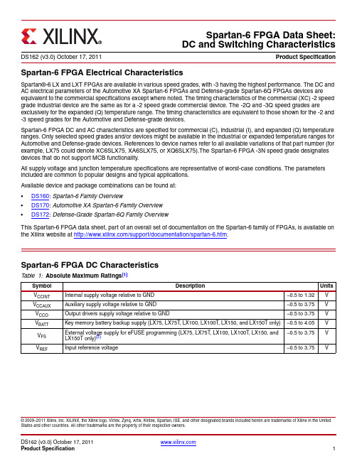
ug388 - Spartan-6 FPGA Memory Controller User Guide
- 格式:pdf
- 大小:1.74 MB
- 文档页数:66

XILINX MCB使用详解说明:本文档将详细讲述赛灵思的DDR2 IP 核的使用流程,目标芯片为Sparten6系列芯片xc6slx25-2fgg484,ISE版本为12.4,MCB版本为3.5。
应用案例为FPGA芯片外带载两片DDR2芯片进行乒乓操作,目的是用一个PLL驱动两个MCB。
术语:ug382,Xilinx的User Guide,Sparten-6 FPGA Clocking ResourcesUG382(v1.4)August24,2010本人技术有限,不足之处请指正,请发到19861011lsf@,也欢迎讨论,QQ383997593,谢谢!一、核的生成1、打开Xilinx CORE Generator工具,找到MCB核(MIG),2、选择版本,这里以3.5为例(尽量选择最新版本),进入Xilinx Memory Interface Generator界面,单击Next,进入下一步;3、选择输出项,输入自定义模块名;单击Next,注意:如果你是修改一个核而不是第一次生成核,会出现如下对话框,单击Yes,这时会覆盖掉一些文件,因此无论你在接下来的步骤中有没有对核的选项进行修改,最后必须点击Generator;4、单击Next,选择Memory Type;注意到图中有个C1、C3,这是因为Xilinx的MCB有部分是属于硬核,引脚是固定的,分别存在于FPGA芯片的BANK1和BANK3,在代码中将看到很多的信号名是以C1_XXX和C3_XXX开头的,这很容易区分是哪个DDR芯片对应的信号名,注意与后面的端口(Port)混淆;5、单击Next,进入DDR2芯片选项模块,先选择存储器,再输入时钟;这里的Memory Part 选择的是自定义的芯片,单击,输入一个自定义的DDR2芯片名,尽量输入芯片的实名而不是自定义名,这样有利于重复使用,不至于将来使用时不知所云,下面的参数可以在你所选的DDR2芯片DATASHEET中找到,输入参数值,保存,这样就可以在找到自定义的存储器了,单击Next;6、选择同上,单击Next;7、Next;8、Next;9、进入端口配置,(1)选择配置模式,单向与双向的意思是指端口是可读、可写,还是既可读又可写,将端口配置成一个读一个写,其他不用;(2)选择存储器的地址映射方式,可根据自己程序设计方便选择,这里默认;10、Next,这里由于对两个DDR2的操作是相同的,配置同上;Next11、Next;12、Next;13、进入FPGA选项,这里注意系统时钟的方式,根据实际情况选择单端还是差分,这里选择单端其他默认;14、Next,同上;15、Next;16、选择Next;17、Next;18、二、IP核内部文件详解该部分主要尝试描述MCB的时钟部分。
Chapter 3Designing with the MCB与MCB的设计本章提供了有关如何设计与系列Spartan®-6 FPGA的详细信息MCB。
它包含以下几个部分:•设计流程•支持的存储设备•仿真•资源利用•时钟•迁移和银行•PCB布局考量设计流程有对MCB的两个支持的设计流程:•非嵌入式设计流程•传统的FPGA设计流程用Xilinx®ISE®工具•MIG工具的核心是发电机™工具中的MCB设计中使用•嵌入式设计流程•处理器为基础与EDK工具流程FPGA系统设计•IP配置在Xilinx平台工作室(XPS)是EDK环境中的MCB设计中使用两个工具流程为开发一种可靠的接口的外部存储器装置的简单方法。
阿一步一步的图形用户界面驱动的流程允许MCB的设计进行配置和参数设置,以满足应用的具体需求。
MIG工具流实际上有两个“包装”水平:低级别封装(mcb_raw_wrapper.v)和顶层的包装(例如,memc3_wrapper.v)。
较低级别的封装集成了所有必要的硅块(MCB,I / O等)和软逻辑(软校准模块)所需的溶液。
它还提供了访问与底层硬件实现的用户界面端口和校准逻辑相关联的所有信号。
顶层的包装器处理信号的重新分配,打结较低级别的包装信号,根据需要,并传递下来的参数值,以根据用户的选择在MIG工具的下包装。
顶级的包装提出了只有那些实现MCB-based设计MIG工具流期间配置所需的信号的一个干净的界面。
例如,在低级别的包装总是显示所有6的用户界面上的原生32位端口,顶级包装重新分配信号,领带关闭不使用的端口,并连接巴士出示Port接口的用户期望,比如一个64位端口。
顶层的包装器是一个被随后集成到更大的FPGA设计。
较低级别的包装(mcb_raw_wrapper.v)是记录在本使用手册。
第2章中的参数和信号列表,例如,都是相对于该下位包装器描述。
基于在MIG工具的GUI流程做出的选择这个包装不改变,而最上层的包装器定制为用户选择的结果。

SP601 Hardware User GuideUG518 (v1.7) September 26, 2012© Copyright 2009–2012 Xilinx, Inc. Xilinx, the Xilinx logo, Artix, ISE, Kintex, Spartan, Virtex, Zynq, and other designated brands included herein are trademarks of Xilinx in the United States and other countries. All other trademarks are the property of their respective owners. DISCLAIMERThe information disclosed to you hereunder (the “Materials”) is provided solely for the selection and use of Xilinx products. To the maximum extent permitted by applicable law: (1) Materials are made available “AS IS” and with all faults, Xilinx hereby DISCLAIMS ALL WARRANTIES AND CONDITIONS, EXPRESS, IMPLIED, OR ST ATUTORY, INCLUDING BUT NOT LIMITED TO WARRANTIES OF MERCHANTABILITY, NON-INFRINGEMENT, OR FITNESS FOR ANY PARTICULAR PURPOSE; and (2) Xilinx shall not be liable (whether in contract or tort, including negligence, or under any other theory of liability) for any loss or damage of any kind or nature related to, arising under, or in connection with, the Materials (including your use of the Materials), including for any direct, indirect, special, incidental, or consequential loss or damage (including loss of data, profits, goodwill, or any type of loss or damage suffered as a result of any action brought by a third party) even if such damage or loss was reasonably foreseeable or Xilinx had been advised of the possibility of the same. Xilinx assumes no obligation to correct any errors contained in the Materials, or to advise you of any corrections or update. Y ou may not reproduce, modify, distribute, or publicly display the Materials without prior written consent. Certain products are subject to the terms and conditions of the Limited Warranties which can be viewed at /warranty.htm; IP cores may be subject to warranty and support terms contained in a license issued to you by Xilinx. Xilinx products are not designed or intended to be fail-safe or for use in any application requiring fail-safe performance; you assume sole risk and liability for use of Xilinx products in Critical Applications:/warranty.htm#critapps.Revision HistoryThe following table shows the revision history for this document.Date Version Revision07/15/09 1.0Initial Xilinx release.08/19/09 1.1•Added Appendix B, VITA 57.1 FMC LPC Connector Pinout.•Updated Figure1-17.•Updated Table1-4, Table1-19, and Table1-22.•Added introductory paragraph to Appendix C, SP601 Master UCF.•Miscellaneous typographical edits and new user guide template.05/17/10 1.2•Updated Figure1-1, Figure1-2, Figure1-14, Figure1-18, Table1-9, Table1-1,Table1-11, and Table1-16.•Added Figure1-7, Figure1-8, and Table1-13.•Updated 9. VITA 57.1 FMC-LPC Connector, page25, Appendix B, VITA 57.1 FMCLPC Connector Pinout, and Appendix C, SP601 Master UCF.06/16/10 1.3Reversed order of 15. Configuration Options and 16. Power Management. Updated 1.Spartan-6 XC6SLX16-2CSG324 FPGA and 2. 128 MB DDR2 Component Memory. AddedTable1-26. Added UG394, Spartan-6 FPGA Power Management User Guide to Appendix D,References.09/24/10 1.4Added Power System Test Points, including Table1-25.02/16/11 1.5Added note and revised header description to indicate the I/Os support LVCMOS25signaling on page34. Revised oscillator manufacturer information from Epson to SiTimeon page page23 and page51.07/18/11 1.6Corrected wording from “PPM frequency jitter” to “PPM frequency stability” in sectionOscillator (Differential), page23. Added Table1-15, page27.09/26/12 1.7Added Regulatory and Compliance Information, page53.SP601 Hardware User Guide UG518 (v1.7) September 26, 2012SP601 Hardware User Guide 3UG518 (v1.7) September 26, 2012Revision History . . . . . . . . . . . . . . . . . . . . . . . . . . . . . . . . . . . . . . . . . . . . . . . . . . . . . . . . . . . . . 2Preface: About This GuideGuide Contents . . . . . . . . . . . . . . . . . . . . . . . . . . . . . . . . . . . . . . . . . . . . . . . . . . . . . . . . . . . . . . 5Additional Documentation . . . . . . . . . . . . . . . . . . . . . . . . . . . . . . . . . . . . . . . . . . . . . . . . . . . 5Additional Support Resources . . . . . . . . . . . . . . . . . . . . . . . . . . . . . . . . . . . . . . . . . . . . . . . . 6Chapter 1: SP601 Evaluation BoardOverview . . . . . . . . . . . . . . . . . . . . . . . . . . . . . . . . . . . . . . . . . . . . . . . . . . . . . . . . . . . . . . . . . . . . 7Additional Information. . . . . . . . . . . . . . . . . . . . . . . . . . . . . . . . . . . . . . . . . . . . . . . . . . . . . 7Features . . . . . . . . . . . . . . . . . . . . . . . . . . . . . . . . . . . . . . . . . . . . . . . . . . . . . . . . . . . . . . . . . . 8Block Diagram . . . . . . . . . . . . . . . . . . . . . . . . . . . . . . . . . . . . . . . . . . . . . . . . . . . . . . . . . . . . 9Related Xilinx Documents . . . . . . . . . . . . . . . . . . . . . . . . . . . . . . . . . . . . . . . . . . . . . . . . . . . . 9Detailed Description . . . . . . . . . . . . . . . . . . . . . . . . . . . . . . . . . . . . . . . . . . . . . . . . . . . . . . . . 101. Spartan-6 XC6SLX16-2CSG324 FPGA. . . . . . . . . . . . . . . . . . . . . . . . . . . . . . . . . . . . . . 11Configuration . . . . . . . . . . . . . . . . . . . . . . . . . . . . . . . . . . . . . . . . . . . . . . . . . . . . . . . . . 11I/O Voltage Rails . . . . . . . . . . . . . . . . . . . . . . . . . . . . . . . . . . . . . . . . . . . . . . . . . . . . . . 122. 128 MB DDR2 Component Memory . . . . . . . . . . . . . . . . . . . . . . . . . . . . . . . . . . . . . . . 123. SPI x4 Flash . . . . . . . . . . . . . . . . . . . . . . . . . . . . . . . . . . . . . . . . . . . . . . . . . . . . . . . . . . . . 154. Linear Flash BPI . . . . . . . . . . . . . . . . . . . . . . . . . . . . . . . . . . . . . . . . . . . . . . . . . . . . . . . . 175. 10/100/1000 Tri-Speed Ethernet PHY . . . . . . . . . . . . . . . . . . . . . . . . . . . . . . . . . . . . . 196. USB-to-UART Bridge. . . . . . . . . . . . . . . . . . . . . . . . . . . . . . . . . . . . . . . . . . . . . . . . . . . . 217. IIC Bus . . . . . . . . . . . . . . . . . . . . . . . . . . . . . . . . . . . . . . . . . . . . . . . . . . . . . . . . . . . . . . . . 228-Kb NV Memory . . . . . . . . . . . . . . . . . . . . . . . . . . . . . . . . . . . . . . . . . . . . . . . . . . . . . . 228. Clock Generation . . . . . . . . . . . . . . . . . . . . . . . . . . . . . . . . . . . . . . . . . . . . . . . . . . . . . . . 23Oscillator (Differential). . . . . . . . . . . . . . . . . . . . . . . . . . . . . . . . . . . . . . . . . . . . . . . . . . 23Oscillator Socket (Single-Ended, 2.5V or 3.3V) . . . . . . . . . . . . . . . . . . . . . . . . . . . . . . . . 24SMA Connectors (Differential). . . . . . . . . . . . . . . . . . . . . . . . . . . . . . . . . . . . . . . . . . . . 249. VITA 57.1 FMC-LPC Connector . . . . . . . . . . . . . . . . . . . . . . . . . . . . . . . . . . . . . . . . . . 2510. Status LEDs. . . . . . . . . . . . . . . . . . . . . . . . . . . . . . . . . . . . . . . . . . . . . . . . . . . . . . . . . . . 2811. FPGA Awake LED and Suspend Jumper. . . . . . . . . . . . . . . . . . . . . . . . . . . . . . . . . . 2912. FPGA INIT and DONE LEDs. . . . . . . . . . . . . . . . . . . . . . . . . . . . . . . . . . . . . . . . . . . . 3013. User I/O . . . . . . . . . . . . . . . . . . . . . . . . . . . . . . . . . . . . . . . . . . . . . . . . . . . . . . . . . . . . . 3114. FPGA_PROG_B Pushbutton Switch . . . . . . . . . . . . . . . . . . . . . . . . . . . . . . . . . . . . . . 3515. Configuration Options . . . . . . . . . . . . . . . . . . . . . . . . . . . . . . . . . . . . . . . . . . . . . . . . . 36JTAG Configuration . . . . . . . . . . . . . . . . . . . . . . . . . . . . . . . . . . . . . . . . . . . . . . . . . . . . 3616. Power Management. . . . . . . . . . . . . . . . . . . . . . . . . . . . . . . . . . . . . . . . . . . . . . . . . . . . 37AC Adapter and 5V Input Power Jack/Switch . . . . . . . . . . . . . . . . . . . . . . . . . . . . . . . . 37Onboard Power Supplies . . . . . . . . . . . . . . . . . . . . . . . . . . . . . . . . . . . . . . . . . . . . . . . . 37Power System Test Points . . . . . . . . . . . . . . . . . . . . . . . . . . . . . . . . . . . . . . . . . . . . . . . . 38Table of ContentsAppendix A: Default Jumper and Switch SettingsAppendix B: VITA 57.1 FMC LPC Connector PinoutAppendix C: SP601 Master UCFAppendix D: ReferencesAppendix E: Regulatory and Compliance InformationDirectives. . . . . . . . . . . . . . . . . . . . . . . . . . . . . . . . . . . . . . . . . . . . . . . . . . . . . . . . . . . . . . . . . . . 53Standards. . . . . . . . . . . . . . . . . . . . . . . . . . . . . . . . . . . . . . . . . . . . . . . . . . . . . . . . . . . . . . . . . . . 53 Electromagnetic Compatibility . . . . . . . . . . . . . . . . . . . . . . . . . . . . . . . . . . . . . . . . . . . . . 53Safety . . . . . . . . . . . . . . . . . . . . . . . . . . . . . . . . . . . . . . . . . . . . . . . . . . . . . . . . . . . . . . . . . . . 53 Markings . . . . . . . . . . . . . . . . . . . . . . . . . . . . . . . . . . . . . . . . . . . . . . . . . . . . . . . . . . . . . . . . . . . 54 SP601 Hardware User GuideUG518 (v1.7) September 26, 2012SP601 Hardware User Guide 5UG518 (v1.7) September 26, 2012PrefaceAbout This GuideThis manual accompanies the Spartan®-6 FPGA SP601 Evaluation Board and contains information about the SP601 hardware and software tools.Guide ContentsThis manual contains the following chapters:•Chapter 1, SP601 Evaluation Board , provides an overview of the SP601 evaluation board and details the components and features of the SP601 board.•Appendix A, Default Jumper and Switch Settings .•Appendix B, VITA 57.1 FMC LPC Connector Pinout .•Appendix C, SP601 Master UCF .•Appendix D, References .Additional DocumentationThe following documents are available for download at /products/spartan6.•Spartan-6 Family OverviewThis overview outlines the features and product selection of the Spartan-6 family.•Spartan-6 FPGA Data Sheet: DC and Switching CharacteristicsThis data sheet contains the DC and switching characteristic specifications for the Spartan-6 family.•Spartan-6 FPGA Packaging and Pinout SpecificationsThis specification includes the tables for device/package combinations and maximum I/Os, pin definitions, pinout tables, pinout diagrams, mechanical drawings, and thermal specifications.•Spartan-6 FPGA Configuration User GuideThis all-encompassing configuration guide includes chapters on configuration interfaces (serial and parallel), multi-bitstream management, bitstream encryption, boundary-scan and JTAG configuration, and reconfiguration techniques.•Spartan-6 FPGA SelectIO Resources User GuideThis guide describes the SelectIO™ resources available in all Spartan-6 devices.•Spartan-6 FPG A Clocking Resources User GuidePreface:About This GuideThis guide describes the clocking resources available in all Spartan-6 devices,including the DCMs and PLLs.•Spartan-6 FPGA Block RAM Resources User GuideThis guide describes the Spartan-6 device block RAM capabilities.•Spartan-6 FPGA DSP48A1 Slice User GuideThis guide describes the architecture of the DSP48A1 slice in Spartan-6FPGAs andprovides configuration examples.•Spartan-6 FPGA Memory Controller User GuideThis guide describes the Spartan-6 FPGA memory controller block, a dedicatedembedded multi-port memory controller that greatly simplifies interfacingSpartan-6FPGAs to the most popular memory standards.•Spartan-6 FPGA PCB Designer’s GuideThis guide provides information on PCB design for Spartan-6 devices, with a focus onstrategies for making design decisions at the PCB and interface level.Additional Support ResourcesTo search the database of silicon and software questions and answers or to create atechnical support case in WebCase, see the Xilinx website at:/support. SP601 Hardware User GuideUG518 (v1.7) September 26, 2012Chapter1 SP601 Evaluation BoardOverviewThe SP601 board enables hardware and software developers to create or evaluate designstargeting the Spartan®-6 XC6SLX16-2CSG324 FPGA.The SP601 provides board features for evaluating the Spartan-6 family that are common tomost entry-level development environments. Some commonly used features include aDDR2 memory controller, a parallel linear flash, a tri-mode Ethernet PHY, general-purposeI/O (GPIO), and a UART. Additional functionality can be added through the VITA 57.1.1expansion connector. Features, page8 provides a general listing of the board features withdetails provided in Detailed Description, page10.Additional InformationAdditional information and support material is located at:•/sp601This information includes:•Current version of this user guide in PDF format•Example design files for demonstration of Spartan-6 FPGA features and technology•Demonstration hardware and software configuration files for the SP601 linear and SPImemory devices•Reference Design Files•Schematics in PDF format and DxDesigner schematic format•Bill of materials (BOM)•Printed-circuit board (PCB) layout in Allegro PCB format•Gerber files for the PCB (Many free or shareware Gerber file viewers are available onthe internet for viewing and printing these files.)•Additional documentation, errata, frequently asked questions, and the latest newsFor information about the Spartan-6 family of FPGA devices, including product highlights,data sheets, user guides, and application notes, see the Spartan-6 FPGA website at/support/documentation/spartan-6.htm.SP601 Hardware User Guide 7 UG518 (v1.7) September 26, 2012Chapter 1:SP601 Evaluation BoardFeaturesThe SP601 board provides the following features (see Figure1-2 and Table1-1):• 1. Spartan-6 XC6SLX16-2CSG324 FPGA• 2. 128 MB DDR2 Component Memory• 3. SPI x4 Flash• 4. Linear Flash BPI• 5. 10/100/1000 Tri-Speed Ethernet PHY•7. IIC Bus•8Kb NV memory•External access 2-pin header•VITA 57.1 FMC-LPC connector•8. Clock Generation•Oscillator (Differential)•Oscillator Socket (Single-Ended, 2.5V or 3.3V)•SMA Connectors (Differential)•9. VITA 57.1 FMC-LPC Connector•10. Status LEDs•FPGA_AWAKE•INIT•DONE•13. User I/O•User LEDs•User DIP switch•User pushbuttons•GPIO male pin header•14. FPGA_PROG_B Pushbutton Switch•15. Configuration Options• 3. SPI x4 Flash (both onboard and off-board)• 4. Linear Flash BPI•JTAG Configuration•16. Power Management•AC Adapter and 5V Input Power Jack/Switch•Onboard Power Supplies SP601 Hardware User GuideUG518 (v1.7) September 26, 2012Related Xilinx DocumentsBlock DiagramFigure1-1 shows a high-level block diagram of the SP601 and its peripherals.Figure 1-1:SP601 Features and BankingRelated Xilinx DocumentsPrior to using the SP601 Evaluation Board, users should be familiar with Xilinx resources.See the following locations for additional documentation on Xilinx tools and solutions:•ISE: /ise•Answer Browser: /support•Intellectual Property: /ipcenterSP601 Hardware User Guide 9 UG518 (v1.7) September 26, 2012SP601 Hardware User GuideUG518 (v1.7) September 26, 2012Chapter 1:SP601 Evaluation BoardDetailed DescriptionFigure 1-2 shows a board photo with numbered features corresponding to Table 1-1 and the section headings in this document.The numbered features in Figure 1-2 correlate to the features and notes listed in Table 1-1.Figure 1-2:SP601 Board PhotoUG518_02_09100912843126137115109141581316Table 1-1:SP601 FeaturesNumberFeatureNotesSchematic Page1 Spartan-6 FP G A XC6SLX16-2CS G 3242DDR2 Component Elpida EDE1116ACBG 1Gb DDR2SDRAM53SPI x4 Flash and Headers SPI select and External Headers 84Linear Flash BPIStrataFlash 8-bit (J3 device), 3 pins shared w/ SPI x481. Spartan-6 XC6SLX16-2CSG 324 FPGAA Xilinx Spartan-6 XC6SLX16-2CSG324 FPGA is installed on the SP601 Evaluation Board.ReferencesSee the Spartan-6 FPGA Data Sheet . [Ref 1]ConfigurationThe SP601 supports configuration in the following modes:•Master SPI x4•Master SPI x4 with off-board device •BPI•JTAG (using the included USB-A to Mini-B cable)For details on configuring the FPGA, see 15. Configuration Options .The Mode DIP switch SW2 is set to M[1:0] = 01 Master SPI default.ReferencesSee the Spartan-6 FPGA Configuration User Guide for more information. [Ref 2]510/100/1000 Ethernet PHY GMII Marvell Alaska PHY76RS232 UART (USB Bridge)Uses CP2103 Serial-to-USB connection 107IICGoes to Header and VITA 57.1 FMC 108Clock, socket, SMA Differential, Single-Ended, Differential 99VITA 57.1 FMC-LPC connector LVDS signals, clocks, PRSNT 610LEDs Ethernet PHY Status711LED, Header FPGA Awake LED, Suspend Header 812LEDs FPGA INIT, DONE 913LED User I/O (active-High)9DIP SwitchUser I/O (active-High)9PushbuttonUser I/O, CPU_RESET (active-High)912-pin (8 I/O) Header6 pins x 2 male header with 8 I/Os (active-High)1014Pushbutton FPGA_PROG_B915USB JTAG Cypress USB to JTAG download cable logic14, 1516Onboard PowerPower Management11,12,13Table 1-1:SP601 Features (Cont’d)NumberFeatureNotesSchematic PageSP601 Hardware User Guide I/O Voltage RailsThere are four available banks on the LX16-CSG324 device. Banks 0, 1, and 2 are connected for 2.5V I/O. Bank 3 is used for the 1.8V DDR2 component memory interface of Spartan-6 FPGA’s hard memory controller. The voltage applied to the FPGA I/O banks used by the SP601 board is summarized in Table 1-2.ReferencesSee the Spartan-6 FPGA documentation for more information at /support/documentation/spartan-6.htm .2. 128 MB DDR2 Component MemoryThere are 128MB of DDR2 memory available on the SP601 board. A 1-Gb ElpidaEDE1116ACBG (84-ball) DDR2 memory component is accessible through Bank 3 of the LX16 device. The Spartan-6 FPGA hard memory controller is used for data transfer across the DDR2 memory interface’s 16-bit data path using SSTL18 signaling. The SP601 board supports the “standard” VCCINT setting of 1.20V ± 5%. This setting provides the standard memory controller block (MCB) performance of 625Mb/s for DDR2 memory in a -2 speed grade device. Signal integrity is maintained through DDR2 resistor terminations and memory on-die terminations (ODT), as shown in Table 1-3 and Table 1-4.Table 1-2:I/O Voltage Rail of FPGA BanksFPGA BankI/O Voltage Rail0 2.5V 1 2.5V 2 2.5V 31.8VTable 1-3:Termination Resistor RequirementsSignal NameBoard TerminationOn-Die TerminationDDR2_A[14:0]49.9Ω to V TT DDR2_BA[2:0]49.9Ω to V TT DDR2_RAS_N 49.9Ω to V TT DDR2_CAS_N 49.9Ω to V TT DDR2_WE_N 49.9Ω to V TT DDR2_CS_N 100Ω to GND DDR2_CKE 4.7K Ω to GND DDR2_ODT 4.7K Ω to GNDDDR2_DQ[15:0]ODT DDR2_UDQS[P ,N], DDR2_LDQS[P ,N]ODT DDR2_UDM, DDR2_LDMODTTable 1-5 shows the connections and pin numbers for the DDR2 Component Memory.DDR2_CK[P ,N]100Ω differential at memorycomponentNotes:1.Nominal value of V TT for DDR2 interface is 0.9V .Table 1-4:FPGA On-Chip (OCT) Termination External Resistor Requirements FPGA U1 PinFPGA Pin NumberBoard Connection for OCTZIO L6No Connect RZQC2100Ω to GROUNDTable 1-5:DDR2 Component Memory ConnectionsFPGA U1 PinSchematic Net Name Memory U2Pin NumberPin NameJ7DDR2_A0M8A0J6DDR2_A1M3A1H5DDR2_A2M7A2L7DDR2_A3N2A3F3DDR2_A4N8A4H4DDR2_A5N3A5H3DDR2_A6N7A6H6DDR2_A7P2A7D2DDR2_A8P8A8D1DDR2_A9P3A9F4DDR2_A10M2A10D3DDR2_A11P7A11G6DDR2_A12R2A12L2DDR2_DQ0G8DQ0L1DDR2_DQ1G2DQ1K2DDR2_DQ2H7DQ2K1DDR2_DQ3H3DQ3H2DDR2_DQ4H1DQ4H1DDR2_DQ5H9DQ5J3DDR2_DQ6F1DQ6Table 1-3:Termination Resistor Requirements (Cont’d)Signal NameBoard Termination On-Die TerminationSP601 Hardware User Guide ReferencesSee the Elpida DDR2 SDRAM Specifications for more information. [Ref 11]Also, see the Spartan-6 FPGA Memory Controller User Guide . [Ref 3]J1DDR2_DQ7F9DQ7M3DDR2_DQ8C8DQ8M1DDR2_DQ9C2DQ9N2DDR2_DQ10D7DQ10N1DDR2_DQ11D3DQ11T2DDR2_DQ12D1DQ12T1DDR2_DQ13D9DQ13U2DDR2_DQ14B1DQ14U1DDR2_DQ15B9DQ15F2DDR2_BA0L2BA0F1DDR2_BA1L3BA1E1DDR2_BA2L1BA2E3DDR2_WE_B K3WE L5DDR2_RAS_B K7RAS K5DDR2_CAS_B L7CAS K6DDR2_ODT K9ODT G3DDR2_CLK_P J8CK G1DDR2_CLK_N K8CK H7DDR2_CKE K2CKE L4DDR2_LDQS_P F7LDQS L3DDR2_LDQS_N E8LDQS P2DDR2_UDQS_P B7UDQS P1DDR2_UDQS_N A8UDQS K3DDR2_LDM F3LDM K4DDR2_UDMB3UDMTable 1-5:DDR2 Component Memory Connections (Cont’d)FPGA U1 PinSchematic Net Name Memory U2Pin NumberPin Name3. SPI x4 FlashThe Xilinx Spartan-6 FPGA hosts a SPI interface which is accessible to the Xilinx iMPACTconfiguration tool. The SPI memory device operates at 3.0V; the Spartan-6 FPGA I/Os are3.3V tolerant and provide electrically compatible logic levels to directly access the SPI flashthrough a 2.5V bank. The XC6SLX16-2CSG324 is a master device when accessing anexternal SPI flash memory device.The SP601 SPI interface has two parallel connected configuration options (see Figure1-4):an SPI X4 (Winbond W25Q64VSFIG) 64-Mb flash memory device and a flashprogramming header (J12). J12 supports a user-defined SPI mezzanine board. The SPIconfiguration source is selected via SPI select jumper J15. For details on configuring theFPGA, see 15. Configuration Options.Figure 1-3:J12 SPI Flash Programming HeaderSP601 Hardware User Guide ReferencesSee the Winbond Serial Flash Memory Data Sheet for more information. [Ref 12]See the XPS Serial Peripheral Interface Data Sheet for more information. [Ref 4]Figure 1-4:SPI Flash Interface TopologyTable 1-6:SPI x4 Memory ConnectionsFPGA U1 PinSchematic Net Name SPI MEM U17SPI HDR J12Pin #Pin NamePinNumberPin NameV2FPGA_PROG_B 1V14FPGA_D2_MISO31IO3_HOLD_B 2T14FPGA_D1_MISO2_R 9IO2_WP_B3V3SPI_CS_B4TMS T13FPGA_MOSI_CSI_B_MISO015DIN 5TDI R13FPGA_D0_DIN_MISO_MISO18IO1_DOUT6TDO R15FPGA_CCLK16CLK7TCK 8GND 9VCC3V3J15.2SPIX4_CS_B 7CS_B4. Linear Flash BPIAn 8-bit (16MB) Numonyx linear flash memory (TE28F128J3D-75) (J3D type) is used toprovide non-volatile bitstream, code, and data storage. The J3D devices operate at 3.0V; theSpartan-6 FPGA I/Os are 3.3V tolerant and provide electrically compatible logic levels todirectly access the linear flash BPI through a 2.5V bank. For details on configuring theFPGA, see 15. Configuration Options.Figure 1-5:Linear Flash BPI InterfaceTable 1-7:BPI Memory ConnectionsFPGA U1 Pin Schematic Net Name BPI Memory U10Pin Number Pin Name K18FLASH_A032A0K17FLASH_A128A1J18FLASH_A227A2J16FLASH_A326A3G18FLASH_A425A4G16FLASH_A524A5H16FLASH_A623A6H15FLASH_A722A7H14FLASH_A820A8H13FLASH_A919A9F18FLASH_A1018A10F17FLASH_A1117A11K13FLASH_A1213A12K12FLASH_A1312A13E18FLASH_A1411A14E16FLASH_A1510A15G13FLASH_A168A16SP601 Hardware User Guide Note:Memory U10 pin 56 address A24 is not connected on the 16 MB device. It is made availablefor larger density devices.ReferencesSee the Numonyx Embedded Flash Memory Data Sheet for more information. [Ref 13]In addition, see the Spartan-6 FPGA Configuration User Guide for more information. [Ref 2]H12FLASH_A177A17D18FLASH_A186A18D17FLASH_A195A19G14FLASH_A204A20F14FLASH_A213A21C18FLASH_A221A22C17FLASH_A2330A23F16FLASH_A2456A24R13FPGA_D0_DIN_MISO_MISO133DQ0T14FPGA_D1_MISO235DQ1V14FPGA_D2_MISO338DQ2U5FLASH_D340DQ3V5FLASH_D444DQ4R3FLASH_D546DQ5T3FLASH_D649DQ6R5FLASH_D751DQ7M16FLASH_WE_B 55WE_B L18FLASH_OE_B 54OE_B L17FLASH_CE_B14CE0B3FMC_PWR_GOOD_FLASH_RST_B16RP_BTable 1-7:BPI Memory Connections (Cont’d)FPGA U1 PinSchematic Net NameBPI Memory U10Pin NumberPin Name5. 10/100/1000 T ri-Speed Ethernet PHYThe SP601 uses the onboard Marvell Alaska PHY device (88E1111) for Ethernetcommunications at 10, 100, or 1000 Mb/s. The board supports a GMII/MII interface fromthe FPGA to the PHY. The PHY connection to a user-provided Ethernet cable is through aHalo HFJ11-1G01E RJ-45 connector with built-in magnetics.On power-up, or on reset, the PHY is configured to operate in GMII mode with PHYaddress 0b00111 using the settings shown in Table1-8. These settings can be overwrittenvia software commands passed over the MDIO interface.Table 1-8:PHY Configuration PinsPin Connection onBoardBit[2]Definition and ValueBit[1]Definition and ValueBit[0]Definition and ValueCFG0V CC 2.5V PHYADR[2] = 1PHYADR[1] = 1PHYADR[0] = 1 CFG1Ground ENA_PAUSE = 0PHYADR[4] = 0PHYADR[3] = 0 CFG2V CC 2.5V ANEG[3] = 1ANEG[2] = 1ANEG[1] = 1 CFG3V CC 2.5V ANEG[0] = 1ENA_XC = 1DIS_125 = 1 CFG4V CC 2.5V HWCFG_MD[2] = 1HWCFG_MD[1] = 1HWCFG_MD[0] = 1 CFG5V CC 2.5V DIS_FC = 1DIS_SLEEP = 1HWCFG_MD[3] = 1 CFG6PHY_LED_RX SEL_BDT = 0INT_POL = 175/50Ω = 0 Table 1-9:Ethernet PHY ConnectionsFPGA U1 Pin Schematic Net NameU3 M88E111Pin Number Pin NameP16PHY_MDIO33MDIO N14PHY_MDC35MDC J13PHY_INT32INT_B L13PHY_RESET36RESET_B M13PHY_CRS115CRS L14PHY_COL114COL L16PHY_RXCLK7RXCLK P17PHY_RXER8RXER N18PHY_RXCTL_RXDV4RXDV M14PHY_RXD03RXD0 U18PHY_RXD1128RXD1 U17PHY_RXD2126RXD2 T18PHY_RXD3125RXD3 T17PHY_RXD4124RXD4 N16PHY_RXD5123RXD5SP601 Hardware User GuideReferencesSee the Marvell Alaska Gigabit Ethernet Transceivers product page for more information.[Ref 16]Also, see the LogiCORE™ IP Tri-Mode Ethernet MAC User Guide . [Ref 5]N15PHY_RXD6121RXD6P18PHY_RXD7120RXD7A9 PHY_TXC_G TPCLK 14G TXCLKB9 PHY_TXCLK 10TXCLK A8 PHY_TXER 13TXER B8 PHY_TXCTL_TXEN 16TXEN F8 PHY_TXD018TXD0G 8 PHY_TXD119TXD1A6 PHY_TXD220TXD2B6 PHY_TXD324TXD3E6 PHY_TXD425TXD4F7 PHY_TXD526TXD5A5 PHY_TXD628TXD6C5 PHY_TXD729TXD7Table 1-9:Ethernet PHY Connections (Cont’d)FPGA U1 PinSchematic Net NameU3 M88E111Pin NumberPin Name6. USB-to-UART BridgeThe SP601 contains a Silicon Labs CP2103GM USB-to-UART bridge device (U4) which allows connection to a host computer with a USB cable. The USB cable is supplied in this evaluation kit (Type A end to host computer, Type Mini-B end to SP601 connector J9). Table 1-10 details the SP601 J9 pinout.Xilinx UART IP is expected to be implemented in the FPGA fabric. The FPGA supports the USB-to-UART bridge using four signal pins, transmit (TX), receive (RX), Request to Send (RTS), and Clear to Send (CTS).Silicon Labs provides royalty-free Virtual COM Port (VCP) drivers which permit the CP2103GM USB-to-UART bridge to appear as a COM port to host computercommunications application software (for example, HyperTerm or TeraTerm). The VCP device driver must be installed on the host PC prior to establishing communications with the SP601. Refer to the SP601 Getting Started Guide for driver installation instructions.ReferencesRefer to the Silicon Labs website for technical information on the CP2103GM and the VCP drivers.In addition, see some of the Xilinx UART IP specifications at:•/support/documentation/ip_documentation/xps_uartlite.pdf •/support/documentation/ip_documentation/xps_uart16550.pdfTable 1-10:USB Type B Pin Assignments and Signal DefinitionsUSB ConnectorPinSignal NameDescription1VBUS +5V from host system (not used)2USB_DATA_N Bidirectional differential serial data (N-side)3USB_DATA_P Bidirectional differential serial data (P-side)4GROUNDSignal groundTable 1-11:CP2103GM ConnectionsFPGA U1 PinUART Functionin FPGA Schematic Net Name U4 CP2103GMPinUART Function in CP2103GM U10RTS, output USB_1_CTS 22CTS, input T5CTS, input USB_1_RTS 23RTS, output L12TX, data out USB_1_RX 24RXD, data in K14RX, data inUSB_1_TX25TXD, data out。
Chapter6 Readback and Configuration VerificationSpartan®-6 devices allow users to read configuration memory through the SelectMAP,ICAP, and JTAG interfaces. During readback, the user reads all configuration memorycells, including the current values on all user memory elements (LUT RAM, SRL16, andblock RAM).To read configuration memory, users must send a sequence of commands to the device toinitiate the readback procedure. Once initiated, the device dumps the contents of itsconfiguration memory to the SelectMAP or JTAG interface. The Accessing ConfigurationRegisters through the SelectMAP Interface section and IEEE Std 1149.1 JTAG describe thesteps for reading configuration memory.Users can send the readback command sequence from a custom microprocessor, CPLD, orFPGA-based system, or use iMPACT to perform JTAG-based readback verify. iMPACT, thedevice programming software provided with the ISE® software by Xilinx, can perform allreadback and comparison functions for Spartan-6 devices and report to the user whetherthere were any configuration errors.Once configuration memory is read from the device, the next step is to determine if thereare any errors by comparing the readback bitstream to the configuration bitstream. TheVerifying Readback Data section explains how this is done.Preparing a Design for ReadbackThere are two mandatory bitstream settings for readback using JTAG or SelectMAP: theBitGen security setting must not prohibit readback (-g Security:none), and bitstreamencryption must not be used. Additionally, if readback is to be performed through theSelectMAP interface, the port must be set to retain its function after configuration bysetting the persist option in BitGen (-g Persist:Yes), otherwise the SelectMAP data pinsrevert to user I/O, precluding further configuration operations. Beyond these security andencryption requirements, no special considerations are necessary to enable readbackthrough the boundary-scan port. Also, these requirements are not necessary when usingreadback via the ICAP. Limitations for readback are:•Performing a readback while the design is in operation (without providing ashutdown command) results in reading back invalid block RAM data. The actualcontents of the block RAM are unaffected.•Performing a readback (with or without a shutdown command) corrupts the contentsof block RAMs configured in 9K mode.Readback Command SequencesSpartan-6 FPGA configuration memory is read from the FDRO (Frame Data Register -Output) configuration register and can be accessed from the JTAG, SelectMAP, and ICAPinterfaces. For the JTAG and SelectMAP interfaces, readback is possible while the FPGAdesign is active or in a shutdown state, although block RAMs cannot be accessed by theuser design while they are being accessed by the configuration logic.Accessing Configuration Registers through the SelectMAP InterfaceTo read configuration memory through the SelectMAP interface, users must set theinterface for write control to send commands to the FPGA, and then switch the interface toread control to read data from the device. Write and read control for the SelectMAPinterface is determined by the RDWR_B input: the SelectMAP data pins are inputs whenthe interface is set for Write control (RDWR_B = 0); they are outputs when the interface isset for Read control (RDWR_B = 1).The CSI_B signal must be deasserted (CSI_B =1) before toggling the RDWR_B signal,otherwise the user causes an abort (refer to SelectMAP ABORT, page157 for details).The procedure for changing the SelectMAP interface from Write to Read Control, or viceversa, is:1.Deassert CSI_B.2.Toggle RDWR_B.RDWR_B = 0: Write controlRDWR_B = 1: Read control3.Assert CSI_B.4.CSI_B is synchronous to CCLK.5.This procedure is illustrated in Figure6-1.Figure 6-1:Changing the SelectMAP Port from Write to Read ControlChapter 7:Reconfiguration and MultiBootGanged Serial Configuration 5.The BIT file must be reformatted into a PROM file before it can be stored on thePROM. Refer to the Generating PROM Files, page79 section.6.On some Xilinx PROMs, the reset polarity is programmable. RESET should beconfigured as active Low when using this setup.7.For ganged serial configuration, all devices must be identical (same IDCODE) andmust be configured with the same bitstream.8.The CCLK net requires Thevenin parallel termination. See Board Layout forConfiguration Clock (CCLK), page56.9.Ganged serial configuration is specific to the Platform Flash (XCFxxS and XCFxxP)PROMs and SPI serial flash only.10.Fallback MultiBoot is not supported in this configuration.There are a number of important considerations for ganged serial configuration:•Startup sequencing(GTS)GTS should be released before DONE or during the same cycle as DONE to ensure all devices are operational when all DONE pins have been released.•Disable the active DONE driver for all devicesFor ganged serial configuration, the active DONE driver must be disabled for alldevices if the DONE pins are tied together, because there can be variations in the startup sequencing of each device. A pull-up resistor is therefore required on thecommon DONE signal.-g DriveDone:no (BitGen option, all devices)•Connect all DONE pins if using a Master deviceIt is important to connect the DONE pins for all devices in ganged serial configuration if one FPGA is used as the Master device. Failing to connect the DONE pins can cause configuration to fail for individual devices in this case. If all devices are set for Slave Serial mode, the DONE pins can be disconnected (if the external CCLK sourcecontinues toggling until all DONE pins go High).For debugging purposes, it is often helpful to have a way of disconnecting individual DONE pins from the common DONE signal.ONE pin rise time•DAfter all DONE pins are released, the DONE pin should rise from logic 0 to logic 1 in one CCLK cycle. If additional time is required for the DONE signal to rise, the BitGen -g DonePipe option can be set for all devices in the serial daisy-chain.•Configuration Clock (CCLK) as the clock signal for board layoutThe CCLK signal is relatively slow, but the edge rates on the Spartan-6 FPGA input buffers are very fast. Even minor signal integrity problems on the CCLK signal can cause the configuration to fail. (Typical failure mode: DONE Low and INIT_B High.) Therefore, design practices that focus on signal integrity, including signal integrity simulation with IBIS, are recommended.•Signal fanoutDesigners must focus on good signal integrity when using ganged serialconfiguration. Signal integrity simulation is recommended.•PROM files for ganged serial configurationPROM files for ganged serial configuration are identical to the PROM files used to configure single devices. There are no special PROM file considerations.。

Chapter 6:Readback and Configuration VerificationThe MSB of all configuration packets sent through the CFG_IN register must be sentfirst. The LSB is shifted while moving the TAP controller out of the SHIFT-DR state.4.Shift the CFG_OUT instruction into the JTAG Instruction Register through the Shift-IRstate. The LSB of the CFG_OUT instruction is shifted first; the MSB is shifted whilemoving the TAP controller out of the SHIFT-IR state.5.Shift 32 bits out of the Status register through the Shift-DR state.6.Reset the TAP controller.Table 6-5:Status Register Readback Command Sequence (JTAG)Step Description Set and Hold# ofClocks(TCK) TDI TMS1Clock five 1s on TMS to bring the device to the TLR state.X15 Move into the RTI state.X01 Move into the Select-IR state.X12 Move into the Shift-IR state.X022Shift the first five bits of the CFG_IN instruction, LSBfirst.00101(CFG_IN)05Shift the MSB of the CFG_IN instruction while exitingSHIFT-IR.011 Move into the SELECT-DR state.X12 Move into the SHIFT-DR state.X023Shift configuration packets into the CFG_IN dataregister, MSB first.a: 0xAA99a: 0x5566b: 0x2901c: 0x2000c: 0x2000d: 0x2000d: 0x20000111Shift the LSB of the last configuration packet whileexiting SHIFT-DR.011 Move into the SELECT-IR state.X13 Move into the SHIFT-IR state.X024Shift the first five bits of the CFG_OUT instruction, LSBfirst.00100(CFG_OUT)05Shift the MSB of the CFG_OUT instruction while exitingShift-IR.011 Move into the SELECT-DR state.X12 Move into the SHIFT-DR state.X02Readback Command SequencesThe packets shifted in to the JTAG CFG_IN register are identical to the packets shifted in through the SelectMAP interface when reading the STAT register through SelectMAP.Configuration Memory Read Procedure (IEEE Std 1149.1 JTAG)The process for reading configuration memory from the FDRO register through the JTAG interface is similar to the process for reading from other registers. However, additional steps are needed to accommodate frame logic. Configuration data coming from the FDRO register pass through the frame buffer, therefore the first frame of readback data is dummy data and should be discarded (refer to the FDRI and FDRO register description). The IEEE Std 1149.1 JTAG readback flow is recommended for most users.1.Reset the TAP controller.2.Shift the CFG_IN instruction into the JTAG Instruction Register. The LSB of theCFG_IN instruction is shifted first; the MSB is shifted while moving the TAP controller out of the SHIFT-IR state.3.Shift packet write commands into the CFG_IN register through the Shift-DR state:a.Write a dummy word to the device.b.Write the synchronization word to the device.c.Write 1 word to CMD register header.d.Specify the length of the data frame to be read back.e.Write the starting frame address to the FAR registers.4.Shift the JSHUTDOWN instruction into the JTAG Instruction Register.5.Move into the RTI state; remain there for 24 TCK cycles to complete the Shutdown sequence. The DONE pin goes Low during the Shutdown sequence.6.Shift the CFG_IN instruction into the JTAG Instruction Register.7.Move to the Shift-DR state and shift packet write commands into the CFG_IN register:a.Write a dummy word to the device.b.Write the synchronization word to the device.c.Write 1 word to CMD register header.d.Specify the length of the data frame to be read back.e.Write the starting frame address to the FAR registers.f.Write the RCFG command to the device.g.Write the read FDRO register Type-1 packet header to the device.5Shift the contents of the STAT register out of the CFG_OUT data register.0x SSSS015Shift the last bit of the STAT register out of the CFG_OUT data register while exiting SHIFT-DR.S 11Move into the Select-IR state.X 13Move into the Shift-IR State.X 026Reset the TAP Controller.X15Table 6-5:Status Register Readback Command Sequence (JTAG) (Cont’d)StepDescriptionSet and Hold# of Clocks (TCK)TDI TMSh.Write two dummy words to the device to flush the packet buffer.The MSB of all configuration packets sent through the CFG_IN register must be sent first. The LSB is shifted while moving the TAP controller out of the SHIFT-DR state.8.Shift the CFG_OUT instruction into the JTAG Instruction Register through theShift-DR state. The LSB of the CFG_OUT instruction is shifted first; the MSB is shifted while moving the TAP controller out of the SHIFT-IR state.9.Shift frame data from the FDRO register through the Shift-DR state.10.Reset the TAP controller.Table 6-6:Shutdown Readback Command Sequence (JTAG)Step Description Set and Hold# of Clocks(TCK) TDI TMS1Clock five 1s on TMS to bring the device to the TLRstate.X15 Move into the RTI state.X01 Move into the Select-IR state.X12 Move into the Shift-IR state.X022Shift the first five bits of the CFG_IN instruction,LSB first.0010105Shift the MSB of the CFG_IN instruction whileexiting Shift-IR.011 Move into the SELECT-DR state.X12 Move into the SHIFT-DR state.X023Shift configuration packets into the CFG_IN dataregister, MSB first.a: 0xFFFFb: 0xAA99b: 0x5566c: 0x30A1d: 0x0007e: 0x2000f: 0x20000111Shift the LSB of the last configuration packet whileexiting SHIFT-DR.011 Move into the SELECT-IR state.X13 Move into the SHIFT-IR state.X024Shift the first five bits of the JSHUTDOWNinstruction, LSB first.0110105Shift the MSB of the JSHUTDOWN instructionwhile exiting SHIFT-IR.0115Move into the RTI state; remain there for 24TCKcycles.X024 Move into the Select-IR state.X12 Move into the Shift-IR state.X02Required Data Spacing between MultiBoot Images。
1. 配置概述Spartan6系列FPGA通过把应用程序数据导入芯片内部存储器完成芯片的配置。
Spart-6 FPGA可以自己从外部非易失性存储器导入编程数据,或者通过外界的微处理器、DSP等对其进行编程。
对以上任何一种情况,都有串行配置和并行配置之分,串行配置可以减少芯片对引脚的要求,并行配置对8bit/16bit Flash或者微处理器来说更合适。
因为Xilinx的FPGA器件的配置数据存储在CMOS 配置锁存器内(CCL),因此Spartan6 FPGA器件上电后必须重新配置。
Spartan6器件有多种配置模式,包括:JTAG配置模式. Master Serial/SPI配置模式(X1,X2,X4). Slave Serial配置模式. Master SelectMAP/BPI配置模式(X8,X16). Slave SelectMAP配置模式(X8,X16)Spartan6系列FPGA的配置模式由引脚M[0:1]的状态决定(详细介绍见Spartan6系列之器件引脚功能详述),在主配置模式中,CCLK默认来自与内部的振荡器,也可以来自外部的GCLK0/USERCCLK.,the BitGen -g ConfigRate选项可以设置内部时钟的振荡频率,默认频率为2MHZ;无论M[0:1]状态如何,JTAG配置始终可用。
对一个FPGA系统来说,可以有多种配置模式,但往往只有一种配置模式最适合自己的目标系统,应该要进行慎重的选择。
当然,FPGA可以重新装载多个镜像文件,因此可以为1片FPGA提供多个配置文件,典型的应用为:当FPGA上电时,装载一个自检的镜像文件,完成自检后重新装载最终的应用程序镜像文件。
这种方法可大大提高FPGA的使用效率。
因为FPGA的外部存储器可以存储多个镜像文件,因此可以通过FPGA正在使用(已装载的镜像)更新外部存储器内容,实现远程镜像更新升级。
1.1. 主模式配置(master mode)由FPGA自身将外部存储器的配置数据装载进内部的模式称为主模式配置;主配置模式的各种连接方式如下图1所示,左侧为串行配置连接方式,右侧为并行配置连接方式。
Spartan-6 FPGA Configurable Logic BlockUser GuideUG384 (v1.1) February 23, 2010Xilinx is disclosing this user guide, manual, release note, and/or specification (the "Documentation") to you solely for use in the development of designs to operate with Xilinx hardware devices. Y ou may not reproduce, distribute, republish, download, display, post, or transmit the Documentation in any form or by any means including, but not limited to, electronic, mechanical, photocopying, recording, or otherwise, without the prior written consent of Xilinx. Xilinx expressly disclaims any liability arising out of your use of the Documentation. Xilinx reserves the right, at its sole discretion, to change the Documentation without notice at any time. Xilinx assumes no obligation to correct any errors contained in the Documentation, or to advise you of any corrections or updates. Xilinx expressly disclaims any liability in connection with technical support or assistance that may be provided to you in connection with the Information.THE DOCUMENTA TION IS DISCLOSED TO YOU “AS-IS” WITH NO WARRANTY OF ANY KIND. XILINX MAKES NO OTHER WARRANTIES, WHETHER EXPRESS, IMPLIED, OR STA TUTORY, REGARDING THE DOCUMENT ATION, INCLUDING ANY WARRANTIES OF MERCHANTABILITY, FITNESS FOR A P ARTICULAR PURPOSE, OR NONINFRINGEMENT OF THIRD-PARTY RIGHTS. IN NO EVENT WILL XILINX BE LIABLE FOR ANY CONSEQUENTIAL, INDIRECT, EXEMPLARY, SPECIAL, OR INCIDENTAL DAMAGES, INCLUDING ANY LOSS OF DATA OR LOST PROFITS, ARISING FROM YOUR USE OF THE DOCUMENTA TION.© 2009–2010 Xilinx, Inc. XILINX, the Xilinx logo, Virtex, Spartan, ISE, and other designated brands included herein are trademarks of Xilinx in the United States and other countries. All other trademarks are the property of their respective owners.Revision HistoryThe following table shows the revision history for this document.Date Version Revision06/24/09 1.0Initial Xilinx release.02/23/10 1.1Clarified the Slice Description section. Added Figure6. Clarifying edits to StorageElements, Initialization, Distributed RAM and Memory (SLICEM only), and FastLookahead Carry Logic sections. Added Using the Latch Function as Logic andInterconnect Resources. Updated parameter names in Table9 and Table10 andFigure35. Updated description T CINA function and description Table12.Spartan-6 FPGA CLB User Guide UG384 (v1.1) February 23, 2010Table of ContentsRevision History . . . . . . . . . . . . . . . . . . . . . . . . . . . . . . . . . . . . . . . . . . . . . . . . . . . . . . . . . . . . . 2Preface: About This GuideAdditional Documentation. . . . . . . . . . . . . . . . . . . . . . . . . . . . . . . . . . . . . . . . . . . . . . . . . . . 5Additional Support Resources. . . . . . . . . . . . . . . . . . . . . . . . . . . . . . . . . . . . . . . . . . . . . . . . 6Spartan-6 FPGA CLBCLB Overview . . . . . . . . . . . . . . . . . . . . . . . . . . . . . . . . . . . . . . . . . . . . . . . . . . . . . . . . . . . . . . . 7Slice Description. . . . . . . . . . . . . . . . . . . . . . . . . . . . . . . . . . . . . . . . . . . . . . . . . . . . . . . . . . . . . 8CLB/Slice Configurations. . . . . . . . . . . . . . . . . . . . . . . . . . . . . . . . . . . . . . . . . . . . . . . . . . 12Look-Up Table (LUT) . . . . . . . . . . . . . . . . . . . . . . . . . . . . . . . . . . . . . . . . . . . . . . . . . . . . . 12Storage Elements . . . . . . . . . . . . . . . . . . . . . . . . . . . . . . . . . . . . . . . . . . . . . . . . . . . . . . . . . 13Distributed RAM and Memory (SLICEM only) . . . . . . . . . . . . . . . . . . . . . . . . . . . . . . . 15Read Only Memory (ROM) . . . . . . . . . . . . . . . . . . . . . . . . . . . . . . . . . . . . . . . . . . . . . . . . 25Shift Registers (SLICEM only) . . . . . . . . . . . . . . . . . . . . . . . . . . . . . . . . . . . . . . . . . . . . . . 25Multiplexers . . . . . . . . . . . . . . . . . . . . . . . . . . . . . . . . . . . . . . . . . . . . . . . . . . . . . . . . . . . . . 30Designing Large Multiplexers . . . . . . . . . . . . . . . . . . . . . . . . . . . . . . . . . . . . . . . . . . . . . . 31Fast Lookahead Carry Logic. . . . . . . . . . . . . . . . . . . . . . . . . . . . . . . . . . . . . . . . . . . . . . . . 33Using the Latch Function as Logic . . . . . . . . . . . . . . . . . . . . . . . . . . . . . . . . . . . . . . . . . . 35 Interconnect Resources. . . . . . . . . . . . . . . . . . . . . . . . . . . . . . . . . . . . . . . . . . . . . . . . . . . . . . 36Spartan-6 FPGA Interconnect Types. . . . . . . . . . . . . . . . . . . . . . . . . . . . . . . . . . . . . . . . . 36Global Controls . . . . . . . . . . . . . . . . . . . . . . . . . . . . . . . . . . . . . . . . . . . . . . . . . . . . . . . . . . 39STARTUP_SPARTAN6 Primitive . . . . . . . . . . . . . . . . . . . . . . . . . . . . . . . . . . . . . . . . . . . 39Interconnect Summary . . . . . . . . . . . . . . . . . . . . . . . . . . . . . . . . . . . . . . . . . . . . . . . . . . . . 39 CLB / Slice Timing Models. . . . . . . . . . . . . . . . . . . . . . . . . . . . . . . . . . . . . . . . . . . . . . . . . . 41Slice (LUT and Storage Element) Timing Models. . . . . . . . . . . . . . . . . . . . . . . . . . . . . . 41Slice Distributed RAM Timing Model (SLICEM only). . . . . . . . . . . . . . . . . . . . . . . . . . 45Slice SRL Timing Model (SLICEM only) . . . . . . . . . . . . . . . . . . . . . . . . . . . . . . . . . . . . . 48Slice Carry-Chain Timing Model (SLICEM and SLICEL only). . . . . . . . . . . . . . . . . . . 50 CLB Primitives. . . . . . . . . . . . . . . . . . . . . . . . . . . . . . . . . . . . . . . . . . . . . . . . . . . . . . . . . . . . . . 52Distributed RAM Primitives . . . . . . . . . . . . . . . . . . . . . . . . . . . . . . . . . . . . . . . . . . . . . . . 52Shift Registers (SRLs) Primitive. . . . . . . . . . . . . . . . . . . . . . . . . . . . . . . . . . . . . . . . . . . . . 54Other Shift Register Applications . . . . . . . . . . . . . . . . . . . . . . . . . . . . . . . . . . . . . . . . . . . 55Multiplexer Primitives . . . . . . . . . . . . . . . . . . . . . . . . . . . . . . . . . . . . . . . . . . . . . . . . . . . . 56Carry Chain Primitive. . . . . . . . . . . . . . . . . . . . . . . . . . . . . . . . . . . . . . . . . . . . . . . . . . . . . 57 Spartan-6 FPGA CLB User Guide 3 UG384 (v1.1) February 23, 2010 Spartan-6 FPGA CLB User GuideUG384 (v1.1) February 23, 2010Preface About This GuideThis guide serves as a technical reference describing the Spartan®-6 FPGA configurablelogic blocks (CLBs). Usually, the logic synthesis software assigns the CLB resourceswithout system designer intervention. It can be advantageous for the designer tounderstand certain CLB details, including the varying capabilities of the look-up tables(LUTs), the physical direction of the carry propagation, the number and distribution of theavailable flip-flops, and the availability of the very efficient shift registers. This guidedescribes these and other features of the CLB in detail.Additional DocumentationThe following documents are also available for download at/support/documentation/spartan-6.htm.•Spartan-6 Family OverviewThis overview outlines the features and product selection of the Spartan-6 family.•Spartan-6 FPGA Data Sheet: DC and Switching CharacteristicsThis data sheet contains the DC and switching characteristic specifications for theSpartan-6 family.•Spartan-6 FPGA Packaging and Pinout SpecificationsThis specification includes the tables for device/package combinations and maximumI/Os, pin definitions, pinout tables, pinout diagrams, mechanical drawings, andthermal specifications.•Spartan-6 FPGA Configuration User GuideThis all-encompassing configuration guide includes chapters on configurationinterfaces (serial and parallel), multi-bitstream management, bitstream encryption,boundary-scan and JTAG configuration, and reconfiguration techniques.•Spartan-6 FPGA SelectIO Resources User GuideThis guide describes the SelectIO™ resources available in all Spartan-6 devices.•Spartan-6FPGA Clocking Resources User GuideThis guide describes the clocking resources available in all Spartan-6 devices,including the DCMs and PLLs.•Spartan-6 FPGA Block RAM Resources User GuideThis guide describes the Spartan-6 device block RAM capabilities.•Spartan-6 FPGA GTP Transceivers User GuideThis guide describes the GTP transceivers available in the Spartan-6 LXT FPGAs. Spartan-6 FPGA CLB User Guide 5 UG384 (v1.1) February 23, 2010Preface:About This Guide•Spartan-6 FPGA DSP48A1 Slice User GuideThis guide describes the architecture of the DSP48A1 slice in Spartan-6FPGAs andprovides configuration examples.•Spartan-6 FPGA Memory Controller User GuideThis guide describes the Spartan-6 FPGA memory controller block, a dedicatedembedded multi-port memory controller that greatly simplifies interfacingSpartan-6FPGAs to the most popular memory standards.•Spartan-6 FPGA PCB Design GuideThis guide provides information on PCB design for Spartan-6 devices, with a focus onstrategies for making design decisions at the PCB and interface level.Additional Support ResourcesTo search the database of silicon and software questions and answers or to create atechnical support case in WebCase, see the Xilinx website at:/support. Spartan-6 FPGA CLB User GuideUG384 (v1.1) February 23, 2010Spartan-6 FPGA CLBCLB OverviewThe Configurable Logic Blocks (CLBs) are the main logic resources for implementingsequential as well as combinatorial circuits. Each CLB element is connected to a switchmatrix for access to the general routing matrix (shown in Figure1). A CLB elementcontains a pair of slices. These two slices do not have direct connections to each other, andeach slice is organized as a column. For each CLB, the slice in the bottom of the CLB islabeled as SLICE(0), and the slice in the top of the CLB is labeled as SLICE(1).Figure 1:Arrangement of Slices within the CLBThe Xilinx tools designate slices with the following definitions. An “X” followed by anumber identifies the position of each slice in a pair as well as the column position of theslice. The “X” number counts slices starting from the bottom in sequence 0, 1 (the first CLBcolumn); 2, 3 (the second CLB column); etc. A “Y” followed by a number identifies a row ofslices. The number remains the same within a CLB, but counts up in sequence from oneCLB row to the next CLB row, starting from the bottom. Figure2 shows four CLBs locatedin the bottom-left corner of the die.Spartan-6 FPGA CLB User Guide 7 UG384 (v1.1) February 23, 2010Figure 2:Row and Column Relationship between CLBs and Slices Slice DescriptionEvery slice contains four logic-function generators (or look-up tables, LUTs) and eightstorage elements. These elements are used by all slices to provide logic and ROM functions(Table1). SLICEX is the basic slice. Some slices, called SLICELs, also contain an arithmeticcarry structure that can be concatenated vertically up through the slice column, and wide-function multiplexers. The SLICEMs contain the carry structure and multiplexers, and addthe ability to use the LUTs as 64-bit distributed RAM and as variable-length shift registers(maximum 32-bit).Table 1:Slice FeaturesFeature SLICEX SLICEL SLICEM6-Input LUTs√√√8 Flip-flops√√√Wide Multiplexers√√Carry Logic√√Distributed RAM√Shift Registers√Each column of CLBs contain two slice columns. One column is a SLICEX column, theother column alternates between SLICEL and SLICEMs. Thus, approximately 50% of theavailable slices are of type SLICEX, while 25% each are SLICEL and SLICEMs. TheXC6SLX4 does not have SLICELs (Table3).SLICEM (shown in Figure3) represents a superset of elements and connections found inall slices. SLICEL is shown in Figure4. SLICEX is shown in Figure5. All eight SR, CE, andCLK inputs are driven by common control inputs. Spartan-6 FPGA CLB User GuideUG384 (v1.1) February 23, 2010Figure 3:Diagram of SLICEMSpartan-6 FPGA CLB User Guide 9 UG384 (v1.1) February 23, 2010Figure 4:Diagram of SLICEL Spartan-6 FPGA CLB User GuideUG384 (v1.1) February 23, 2010Figure 5:Diagram of SLICEXSpartan-6 FPGA CLB User Guide CLB/Slice ConfigurationsTable 2 summarizes the logic resources in one CLB. Each CLB or slice can be implemented in one of the configurations listed.Table 3 shows the available CLB resources for the Spartan-6 FPGAs. The ratio between the number of 6-input LUTs and logic cells is 1.6. This reflects the increased capability of the new 6-input LUT architecture compared to traditional 4-input LUTs.Look-Up T able (LUT)The function generators in Spartan-6 FPGAs are implemented as six-input look-up tables(LUTs). There are six independent inputs (A inputs - A1 to A6) and two independentoutputs (O5 and O6) for each of the four function generators in a slice (A, B, C, and D). The function generators can implement any arbitrarily defined six-input Boolean function. Each function generator can also implement two arbitrarily defined five-input Boolean functions, as long as these two functions share common inputs. Only the O6 output of the function generator is used when a six-input function is implemented. Both O5 and O6 are used for each of the five-input function generators implemented. In this case, A6 is drivenTable 2:Logic Resources in One CLB Slices LUTs Flip-FlopsArithmetic and Carry Chains (2)Distributed RAM (1)Shift Registers (1)28161256 bits128 bitsNotes:1.SLICEM only, SLICEL and SLICEX do not have distributed RAM or shift registers.2.SLICEM and SLICEL only.Table 3:Spartan-6 FPGA Logic ResourcesDevice Logic Cells Total Slices SLICEMs SLICELs SLICEXs Number of 6-Input LUTs Maximum Distributed RAM (Kb)ShiftRegisters(Kb)Number ofFlip-FlopsXC6SLX43,84060030003002,40075384,800XC6SLX99,1521,4303603557155,720904511,440XC6SLX1614,5792,2785445951,1399,1121366818,224XC6SLX2524,0513,7589169631,87915,03222911530,064XC6SLX4543,6616,8221,6021,8093,41127,28840120054,576XC6SLX7574,63711,6622,7683,0635,83146,64869234693,296XC6SLX100101,26115,8223,9044,0077,91163,288976488126,576XC6SLX150147,44323,0385,4206,09911,51992,1521,355678184,304XC6SLX25T 24,0513,7589169631,87915,03222911530,064XC6SLX45T 43,6616,8221,6021,8093,41127,28840120054,576XC6SLX75T 74,63711,6622,7683,0635,83146,64869234693,296XC6SLX100T 101,26115,8223,9044,0077,91163,288976488126,576XC6SLX150T147,44323,0385,4206,09911,51992,1521,355678184,304High by the software. The propagation delay through a LUT is independent of the functionimplemented, or whether one six-input or two five-input generators are implemented.Signals from the function generators can exit the slice (through A, B, C, D output for O6 orAMUX, BMUX, CMUX, DMUX output for O5), enter the XOR dedicated gate from an O6output (see Fast Lookahead Carry Logic), enter the carry-logic chain from an O5 output(see Fast Lookahead Carry Logic), enter the select line of the carry-logic multiplexer froman O6 output (see Fast Lookahead Carry Logic), feed the D input of the storage element, orgo to F7AMUX/F7BMUX from an O6 output.Figure6 shows a simplified view of the connectivity for a single LUT6.Figure 6:LUT6In addition to the basic LUTs, SLICEL and SLICEM contain three multiplexers (F7AMUX,F7BMUX, and F8MUX). These multiplexers are used to combine up to four functiongenerators to provide any function of seven or eight inputs in a slice. F7AMUX andF7BMUX are used to generate seven input functions from slice A and B, or C and D, whileF8MUX is used to combine all slices to generate eight input functions. Functions with morethan eight inputs can be implemented using multiple slices. There are no directconnections between slices to form function generators greater than eight inputs within aCLB or between slices, but CLB outputs can be routed through the switch matrix anddirectly back into the CLB inputs.Storage ElementsEach slice has eight storage elements. There are four storage elements in a slice that can beconfigured as either edge-triggered D-type flip-flops or level-sensitive latches. The D inputcan be driven directly by a LUT output via AFFMUX, BFFMUX, CFFMUX or DFFMUX, orby the BYPASS slice inputs bypassing the function generators via AX, BX, CX, or DX input.When configured as a latch, the latch is transparent when the CLK is Low.In Spartan-6 devices, there are four additional storage elements that can only be configuredas edge-triggered D-type flip-flops. The D input can be driven by the O5 output of the LUT.When the original 4 storage elements are configured as latches, these 4 additional storageelements can not be used.Figure7 shows both the register only and the register/latch configuration in a slice, bothare available.Figure 7:Configuration in a Slice: 4 Registers Only and 4 Register/LatchThe control signals clock (CLK), clock enable (CE), and set/reset (SR) are common to allstorage elements in one slice. When one flip-flop in a slice has SR or CE enabled, the otherflip-flops used in the slice will also have SR or CE enabled by the common signal. Only theCLK signal has independent polarity but applies it to all eight storage elements. Anyinverter placed on the clock signal is automatically absorbed. The CE and SR signals areactive High. All flip-flop and latch primitives have CE and non-CE versions. The SR signalalways has priority over CE.InitializationThe SR signal forces the storage element into the initial state specified by SRINIT1 orSRINIT0. SRINIT1 forces a logic High at the storage element output when SR is asserted,while SRINIT0 forces a logic Low at the storage element output (see Table4). Spartan-6 FPGA CLB User GuideSRINIT0 and SRINIT1 can be set individually for each storage element in a slice. The choiceof synchronous (SYNC) or asynchronous (ASYNC) set/reset (SRTYPE) is common to all eight storage elements and cannot be set individually for each storage element in a slice.The initial state after configuration or global initial state is also defined by the same SRINIT option. The initial state is set whenever the Global Set/Reset (GSR) signal is asserted. The GSR signal is always asserted during configuration, and can be controlled after configuration by using the STARTUP_SPARTAN6 primitive. To maximize design flexibility and utilization, use the GSR and avoid local initialization signals.The initial state of any storage element (SRINIT) is defined in the design either by the INIT attribute or by the use of a set or reset. If both methods are used, they must both be 0 or both be 1. INIT =0 or a reset selects SRINIT0, and INIT =1 or a set selects SRINIT1.The storage element must be initialized to the same value both by the global power-up or GSR signal, and by the local SR input to the slice. A storage element cannot have both set and reset, unless one is defined as a synchronous function so that it can be placed in the LUT. Avoid instantiating primitives with the control input while specifying the INIT attribute in an opposite state, for example, an FDRE with a reset input and the INITattribute set to 1. Care should be taken when re-targeting designs from another technology to the Spartan-6 architecture. If converting an existing FPGA design, avoid primitives that use both set and reset, such as the FDCPE primitive.Each of the eight flip-flops in a slice must use the same SR input, although they can be initialized to different values. A second initialization control will require implementation in a separate slice, so minimize the number of initialization signals. The SR could be turned off for all flip-flops in a slice and implemented independently for each flip-flop by implementing it synchronously in the LUT.The SR signal is available to the flip-flop, independent of whether the LUT is used as a distributed RAM or shift register, which supports a registered read from distributed RAM or an additional pipeline stage in a shift register while still allowing initialization.The configuration options for the set and reset functionality of a register or the four storage elements capable of functioning as a latch are as follows:•No set or reset •Synchronous set •Synchronous reset •Asynchronous set (preset)•Asynchronous reset (clear)Distributed RAM and Memory (SLICEM only)The function generators in SLICEMs add a data input and write enable that allows the function generator to be implemented as distributed RAM. RAM resources areTable 4:Truth Table When Using SRINIT SR SRINIT Function 0SRINIT0 (default)No Logic Change1SRI NI T0 (default)0SRINIT1No Logic Change1SRINIT11Spartan-6 FPGA CLB User Guide configurable within a SLICEM to implement the distributed RAM shown in Table 5. Multiple LUTs in a SLICEM can be combined in various ways to store more data.Distributed RAM is fast, localized, and ideal for small data buffers, FIFOs, or register files. For larger memory requirements, consider using the 18K block RAM resources.Distributed RAM are synchronous (write) and asynchronous (read) resources. However, a synchronous read resource can be implemented with a storage element or a flip-flop in the same slice. By placing this flip-flop, the distributed RAM performance is improved by decreasing the delay into the clock-to-out value of the flip-flop. However, an additional clock latency is added. The distributed resources share the same clock input. For a write operation, the Write Enable (WE) input, driven by either the CE or WE pin of a SLICEM, must be set High.Table 5 shows the number of LUTs (four per slice) occupied by each distributed RAM configuration.For single-port configurations, distributed RAM has a common address port forsynchronous writes and asynchronous reads. For dual-port configurations, distributed RAM has one port for synchronous writes and asynchronous reads, and another port for asynchronous reads. In simple dual-port configuration, there is no data out (read port) from the write port. For quad-port configurations, distributed RAM has one port forsynchronous writes and asynchronous reads, and three additional ports for asynchronous reads.In single-port mode, read and write addresses share the same address bus. In dual-port mode, one function generator is connected with the shared read and write port address. The second function generator has the A inputs connected to a second read-only port address and the WA inputs shared with the first read/write port address.Figure 8 through Figure 16 illustrate various example distributed RAM configurations occupying one SLICEM. When using x2 configuration (RAM32X2Q), A6 and WA6 are driven High by the software to keep O5 and O6 independent.Table 5:Distributed RAM ConfigurationRAM Number of LUTsDescription32 x 2Q (2)4Quad-Port 32 x 2-bit RAM 32 x 6SDP (2)4Simple Dual-Port 32 x 6-bit RAM 64 x 1S 1Single-Port 64 x 1-bit RAM 64 x 1D 2Dual-Port 64 x 1-bit RAM 64 x 1Q (3)4Quad-Port 64 x 1-bit RAM 64 x 3SDP (3)4Simple Dual-Port 64 x 3-bit RAM 128 x 1S 2Single-Port 128 x 1-bit RAM 128 x 1D 4Dual-Port 128 x 1-bit RAM 256 x 1S4Single-Port 256 x 1-bit RAMNotes:1.S = single-port configuration; D = dual-port configuration; Q = quad-port configuration; SDP = simple dual-port configuration.2.RAM32M is the associated primitive for this configuration.3.RAM64M is the associated primitive for this configuration.Figure 8:Distributed RAM (RAM32X2Q)Figure 9:Distributed RAM (RAM32X6SDP) Spartan-6 FPGA CLB User GuideFigure 10:Distributed RAM (RAM64X1S)If four single-port 64 x 1-bit modules are built, the four RAM64X1S primitives can occupy a SLICEM, as long as they share the same clock, write enable, and shared read and write port address inputs. This configuration equates to 64 x 4-bit single-port distributed RAM.Figure 11:Distributed RAM (RAM64X1D)If two dual-port 64 x 1-bit modules are built, the two RAM64X1D primitives can occupy a SLICEM, as long as they share the same clock, write enable, and shared read and write port address inputs. This configuration equates to 64 x 2-bit dual-port distributed RAM.Figure 12:Distributed RAM (RAM64X1Q) Spartan-6 FPGA CLB User GuideFigure 13:Distributed RAM (RAM64X3SDP)Implementation of distributed RAM configurations with depth greater than 64 requires the usage of wide-function multiplexers (F7AMUX, F7BMUX, and F8MUX).Figure 14:Distributed RAM (RAM128X1S)If two single-port 128x1-bit modules are built, the two RAM128X1S primitives can occupya SLICEM, as long as they share the same clock, write enable, and shared read and writeport address inputs. This configuration equates to 128x2-bit single-port distributed RAM. Spartan-6 FPGA CLB User GuideFigure 15:Distributed RAM (RAM128X1D)Figure 16:Distributed RAM (RAM256X1S)Distributed RAM configurations larger than the examples provided in Figure8 throughFigure16 require more than one SLICEM. There are no direct connections to form largerdistributed RAM configurations within a CLB or between slices.Using distributed RAM for memory depths of 64 bits or less is generally more efficientthan block RAM in terms of resources, performance, and power. For depths greater than 64bits but less than or equal to 128 bits, use the following guidelines:•To conserve LUT resources, use any extra block RAM•For asynchronous read capability, use distributed RAM•For widths greater than 16 bits, use block RAM Spartan-6 FPGA CLB User Guide•For shorter clock-to-out timing and fewer placement restrictions, use registered distributed RAMDistributed RAM Data FlowSynchronous Write OperationThe synchronous write operation is a single clock-edge operation with an active-Highwrite-enable (WE) feature. When WE is High, the input (D) is loaded into the memorylocation at address A.Asynchronous Read OperationThe output is determined by the address A (for single-port mode output/SPO output ofdual-port mode), or address DPRA (DPO output of dual-port mode). Each time a newaddress is applied to the address pins, the data value in the memory location of thataddress is available on the output after the time delay to access the LUT. This operation isasynchronous and independent of the clock signal.Distributed RAM Summary•Single-port and dual-port modes are available in SLICEMs.• A write operation requires one clock edge.•Read operations are asynchronous (Q output).•The data input has a setup-to-clock timing specification.Read Only Memory (ROM)Each function generator can implement a 64 x 1-bit ROM. Three configurations areavailable: ROM64x1, ROM128x1, and ROM256x1. ROM contents are loaded at each deviceconfiguration. Table6 shows the number of LUTs occupied by each ROM configuration.Table 6:ROM ConfigurationROM Number of LUTs64 x 11128 x 12256 x 14Shift Registers (SLICEM only)A SLICEM function generator can also be configured as a 32-bit shift register without usingthe flip-flops available in a slice. Used in this way, each LUT can delay serial dataanywhere from one to 32 clock cycles. The shiftin D (DI1 LUT pin) and shiftout Q31 (MC31LUT pin) lines cascade LUTs to form larger shift registers. The four LUTs in a SLICEM arethus cascaded to produce delays up to 128 clock cycles. It is also possible to combine shiftregisters across more than one SLICEM. Note that there are no direct connections betweenslices to form longer shift registers, nor is the MC31 output at LUT B/C/D available. Theresulting programmable delays can be used to balance the timing of data pipelines.Applications requiring delay or latency compensation use these shift registers to developefficient designs. Shift registers are also useful in synchronous FIFO and contentaddressable memory (CAM) designs.。
标题:Spartan6 FPGA 读写DDR3出现有规律的错误?问题描述:1、我在调试DDR3时,用了一片MT41JM16JT-15E的DDR3,此片FLASH与SP605开发板相比MT41JM16JT-187E(本来想定此款的,但是此款没有工业级的)。
遇到了如下几个问题:●用了MIG生成之后DDR3控制器之后,参考ug388和ug416,按照步骤发现数据全部正确的,灯也正常。
●在XPS中修改原有基于SP605的设计,其结果如下:BEGIN mpmcPARAMETER INSTANCE = MCB_DDR3PARAMETER C_NUM_PORTS = 1PARAMETER C_PORT_CONFIG = 1PARAMETER C_MCB_LOC = MEMC3PARAMETER C_MEM_CALIBRA TION_SOFT_IP = TRUEPARAMETER C_MEM_SKIP_IN_TERM_CAL = 0PARAMETER C_MEM_SKIP_DYNAMIC_CAL = 0PARAMETER C_MCB_RZQ_LOC = K7PARAMETER C_MCB_ZIO_LOC = M7PARAMETER C_MEM_TYPE = DDR3PARAMETER C_MEM_PARTNO = CUSTOMPARAMETER C_MEM_ODT_TYPE = 1PARAMETER C_MEM_DATA_WIDTH = 16PARAMETER C_PIM0_BASETYPE = 2PARAMETER HW_VER = 6.03.aPARAMETER C_MPMC_BASEADDR = 0x88000000PARAMETER C_MPMC_HIGHADDR = 0x8FFFFFFFPARAMETER C_MEM_PART_DATA_DEPTH = 64PARAMETER C_MEM_PART_DATA_WIDTH = 16PARAMETER C_MEM_PART_NUM_BANK_BITS = 3PARAMETER C_MEM_PART_NUM_ROW_BITS = 13PARAMETER C_MEM_PART_NUM_COL_BITS = 10PARAMETER C_MEM_PART_CAS_A_FMAX = 333PARAMETER C_MEM_PART_CAS_A = 5PARAMETER C_MEM_PART_TRRD = 7500PARAMETER C_MEM_PART_TRCD = 13500PARAMETER C_MEM_PART_TCCD = 4PARAMETER C_MEM_PART_TWR = 15000PARAMETER C_MEM_PART_TWTR = 7500PARAMETER C_MEM_PART_TREFI = 7800000PARAMETER C_MEM_PART_TRFC = 110000PARAMETER C_MEM_PART_TRP = 13500PARAMETER C_MEM_PART_TRC = 49500PARAMETER C_MEM_PART_TRASMAX = 70200000PARAMETER C_MEM_PART_TRAS = 36000BUS_INTERFACE SPLB0 = mb_plbPORT MPMC_Clk0 = clk_66_6667MHzPLL0PORT MPMC_Rst = sys_periph_resetPORT MPMC_Clk_Mem_2x = clk_666_6667MHzPLL0_nobufPORT MPMC_Clk_Mem_2x_180 = clk_666_6667MHz180PLL0_nobufPORT MPMC_PLL_Lock = Dcm_all_lockedPORT mcbx_dram_addr = fpga_0_MCB_DDR3_mcbx_dram_addr_pinPORT mcbx_dram_ba = fpga_0_MCB_DDR3_mcbx_dram_ba_pinPORT mcbx_dram_ras_n = fpga_0_MCB_DDR3_mcbx_dram_ras_n_pinPORT mcbx_dram_cas_n = fpga_0_MCB_DDR3_mcbx_dram_cas_n_pinPORT mcbx_dram_we_n = fpga_0_MCB_DDR3_mcbx_dram_we_n_pinPORT mcbx_dram_cke = fpga_0_MCB_DDR3_mcbx_dram_cke_pinPORT mcbx_dram_clk = fpga_0_MCB_DDR3_mcbx_dram_clk_pinPORT mcbx_dram_clk_n = fpga_0_MCB_DDR3_mcbx_dram_clk_n_pinPORT mcbx_dram_dq = fpga_0_MCB_DDR3_mcbx_dram_dq_pinPORT mcbx_dram_dqs = fpga_0_MCB_DDR3_mcbx_dram_dqs_pinPORT mcbx_dram_dqs_n = fpga_0_MCB_DDR3_mcbx_dram_dqs_n_pinPORT mcbx_dram_udqs = fpga_0_MCB_DDR3_mcbx_dram_udqs_pinPORT mcbx_dram_udqs_n = fpga_0_MCB_DDR3_mcbx_dram_udqs_n_pinPORT mcbx_dram_udm = fpga_0_MCB_DDR3_mcbx_dram_udm_pinPORT mcbx_dram_ldm = fpga_0_MCB_DDR3_mcbx_dram_ldm_pinPORT mcbx_dram_odt = fpga_0_MCB_DDR3_mcbx_dram_odt_pinPORT mcbx_dram_ddr3_rst = fpga_0_MCB_DDR3_mcbx_dram_ddr3_rst_pinPORT rzq = fpga_0_MCB_DDR3_rzq_pinPORT zio = fpga_0_MCB_DDR3_zio_pinEND但是程序进入DDR3运行时发现程序跑飞。
Spartan-6 FPGA Memory ControllerUser GuideUG388 (v2.3) August 9, 2010Xilinx is disclosing this user guide, manual, release note, and/or specification (the "Documentation") to you solely for use in the development of designs to operate with Xilinx hardware devices. Y ou may not reproduce, distribute, republish, download, display, post, or transmit the Documentation in any form or by any means including, but not limited to, electronic, mechanical, photocopying, recording, or otherwise, without the prior written consent of Xilinx. Xilinx expressly disclaims any liability arising out of your use of the Documentation. Xilinx reserves the right, at its sole discretion, to change the Documentation without notice at any time. Xilinx assumes no obligation to correct any errors contained in the Documentation, or to advise you of any corrections or updates. Xilinx expressly disclaims any liability in connection with technical support or assistance that may be provided to you in connection with the Information.THE DOCUMENTA TION IS DISCLOSED TO YOU “AS-IS” WITH NO WARRANTY OF ANY KIND. XILINX MAKES NO OTHER WARRANTIES, WHETHER EXPRESS, IMPLIED, OR STA TUTORY, REGARDING THE DOCUMENT ATION, INCLUDING ANY WARRANTIES OF MERCHANTABILITY, FITNESS FOR A P ARTICULAR PURPOSE, OR NONINFRINGEMENT OF THIRD-PARTY RIGHTS. IN NO EVENT WILL XILINX BE LIABLE FOR ANY CONSEQUENTIAL, INDIRECT, EXEMPLARY, SPECIAL, OR INCIDENTAL DAMAGES, INCLUDING ANY LOSS OF DATA OR LOST PROFITS, ARISING FROM YOUR USE OF THE DOCUMENTA TION.© Copyright 2009–2010 Xilinx, Inc. XILINX, the Xilinx logo, Virtex, Spartan, ISE, and other designated brands included herein are trademarks of Xilinx in the United States and other countries. PCI, PCI Express, PCIe, and PCI-X are trademarks of PCI-SIG. All other trademarks are the property of their respective owners.Revision HistoryThe following table shows the revision history for this document.Date Version Revision05/28/09 1.0Initial Xilinx release.08/18/09 1.1•Removed references to MCB per-bit deskew calibration.•Chapter1:•Added XC6SLX75 and XC6SLX75T devices and CPG196, CSG484, and FG(G)900packages to Table1-2, page13.•Chapter2:•In Figure2-2, page18, changed Configuration 5 to 128-bit bidirectional.•Added note regarding board design requirements under Table2-9, page30.•Chapter3:•Updated first paragraph in Supported Memory Devices, page35.•Added note to Clocking, page37.•Added subsection Additional Board Design Requirements, page42.•Chapter4:•Moved Note 1 from Figure4-1, page46 to below the figure.•Added Note 2 about calibration logic.•Appendix A:•Updated JEDEC specification links in Memory Standards, page65.Spartan-6 FPGA Memory Controller UG388 (v2.3) August 9, 201012/02/09 2.0•Moved Chapter 3, “Getting Started,” and Chapter 6, “Debugging MCB Designs,” andto UG416, Spartan-6 FPGA Memory Interface Solutions User Guide.•Changed introduction in About This Guide, page7.•Chapter1:•Revised Note 1 in Table1-1, page12 to refer to the data sheet for specific values.•Added Note 2 to Table1-2, page13.•Chapter2:•In Table2-3, changed the description and values of theC_MC_CALIBRATION_MODE attribute on page25.•Appended two sentences to exception (a) on page30.•Chapter3:•Replaced text regarding the speed of the calibration clock, calib_clk, on page39.•Chapter4:•Rephrased Note 1 under Figure4-1, page46.•In the third paragraph after the Notes on page46, removed the sentence aboutcalibration logic.•Added note after first paragraph of Calibration, page47.•Removed portion of sentence about calibration logic in first paragraph of Phase 2:DQS Centering, page48.•Added paragraph above Figure4-13, page59.•Added note on page62 before Table4-5.01/05/10 2.0.1Revised document hyperlinks.03/04/10 2.1Chapter1: In the Features and Benefits section, added bullet for input terminationautomatic calibration to section. In Table1-1, added parameters in Data Rate Minimumcolumn and updated table note 2. In Table1-2, revised table note 1.Chapter2: In Table2-2, added “THREEQUARTERS” as a possible value for the MemoryDrive Strength attribute, and modified the description for Memory Burst Lengthattribute, indicating that DDR3 is always set to 8. In the Clock, Reset, and CalibrationSignals section, added calibration to the heading name, introductory text, and caption ofTable2-4. In Table2-4, changed the signal name BUFPLL to BUFPLL_MCB, changed thesignal name sys_rst to async_rst, and added signals mcb_drp_clk and calib_done. In theMemory Device Interface section, modified descriptive text related to RZG and ZIO pins.Added clarifying text in Note (page30) relating to unused pins from an active MCBreverting to general-purpose I/O. In Table2-9, modified descriptions for the rzq and ziosignals.Chapter3: In Table3-1, removed memory devices MT41K128M8xx-25 andMT41K256M4xx-25. In the Clocking section, added text related to MIG/EDK generationof clocking infrastructure. Clarified text related to location of externally driven PLL.Revised text related to calibration clock. In Figure3-3, changed signal name fromcalib_clk to mcb_drp_clk. Changed the end of the first sentence after Figure3-3.Changed the first sentence about the calibration related clock on page39. UnderFigure3-4, added clarifying text related to using bank1 MCB pins as BPI pins. In theAdditional Board Design Requirements section on page43, clarified requirements forpull-down resistors on the RESET, CKE, and ODT signals. Added SimultaneousSwitching Output Considerations section.Chapter4: In the Phase 1: Input Termination section, added clarifying text related toinput termination of the RZQ and ZIO pins. In the Addressing section, added clarifyingtext related to offsetting the starting address location using the write data mask inputs.Added the Read Latency and Suspend sections.Appendix A: Updated JEDEC URLs.UG388 (v2.3) August 9, Spartan-6 FPGA Memory Controller06/14/10 2.2XCN10024, MCB Performance and JTAG Revision Code for Spartan-6 LX16 and LX45 FPGAs,addresses these changes:Chapter1: Added an important note about Standard and Extended performance modes.Chapter2: In Table2-4, included the BUFPLL_MCB block name in the pll_lockdescription and changed the clock frequency example in the sysclk_2x description.Chapter3: In Clocking, removed LOCKED and pll_lock from the PLL block and MIGWrapper blocks, respectively, and changed the clock frequency examples in the secondand fourth paragraphs under Figure3-3 on page38.08/09/10 2.3Chapter1: In Table1-1, changed the minimum data rate value for LPDDR and indicatedthat -3N speed-grade devices do not support the MCB in table note 1. Added table noteto Table1-3.Chapter2: In Table2-4, added italicized sentence to the calib_done signal description. InTable2-5, Table2-6, and Table2-7, added sentence about reset being required to recoverto the pX_cmd_error, pX_wr_error, and pX_rd_error descriptions, respectively.Chapter3: Added BUFG in Figure3-3. Added sentences about preferred PLL location tothe end of the first paragraph under Figure3-3. Added sentences about driving MCBson both sides of the device to the end of the second paragraph under Figure3-3. AddedModifying the Clock Setup section. Added fourth bullet about V REF to Additional BoardDesign Requirements.Chapter4: In the second to the last paragraph of Phase 1: Input Termination, replacedsentence about V REF source still being provided for different I/O standards when acalibrated input termination is desired with sentence about LPDDR memory notrequiring V REF. Added sentence about resulting input termination to the last paragraphof Phase 1: Input Termination on page47.Appendix A: Removed obsolete link.Spartan-6 FPGA Memory Controller UG388 (v2.3) August 9, 2010Spartan-6 FPGA Memory Controller 5UG388 (v2.3) August 9, 2010Revision History . . . . . . . . . . . . . . . . . . . . . . . . . . . . . . . . . . . . . . . . . . . . . . . . . . . . . . . . . . . . . 2Preface: About This GuideGuide Contents . . . . . . . . . . . . . . . . . . . . . . . . . . . . . . . . . . . . . . . . . . . . . . . . . . . . . . . . . . . . . . 7Additional Documentation . . . . . . . . . . . . . . . . . . . . . . . . . . . . . . . . . . . . . . . . . . . . . . . . . . . 7Additional Support Resources . . . . . . . . . . . . . . . . . . . . . . . . . . . . . . . . . . . . . . . . . . . . . . . . 8Chapter 1: Memory Controller Block OverviewScope . . . . . . . . . . . . . . . . . . . . . . . . . . . . . . . . . . . . . . . . . . . . . . . . . . . . . . . . . . . . . . . . . . . . . . . . 9Introduction . . . . . . . . . . . . . . . . . . . . . . . . . . . . . . . . . . . . . . . . . . . . . . . . . . . . . . . . . . . . . . . . . 9Features and Benefits . . . . . . . . . . . . . . . . . . . . . . . . . . . . . . . . . . . . . . . . . . . . . . . . . . . . . . . . 9Block Diagram . . . . . . . . . . . . . . . . . . . . . . . . . . . . . . . . . . . . . . . . . . . . . . . . . . . . . . . . . . . . . . 10Performance . . . . . . . . . . . . . . . . . . . . . . . . . . . . . . . . . . . . . . . . . . . . . . . . . . . . . . . . . . . . . . . .12Device Family Support . . . . . . . . . . . . . . . . . . . . . . . . . . . . . . . . . . . . . . . . . . . . . . . . . . . . . . 13Supported Memory Configurations . . . . . . . . . . . . . . . . . . . . . . . . . . . . . . . . . . . . . . . . . . 14Software and Tool Support . . . . . . . . . . . . . . . . . . . . . . . . . . . . . . . . . . . . . . . . . . . . . . . . . . 14Chapter 2: MCB Functional DescriptionArchitecture Overview . . . . . . . . . . . . . . . . . . . . . . . . . . . . . . . . . . . . . . . . . . . . . . . . . . . . . . 15Port Configurations . . . . . . . . . . . . . . . . . . . . . . . . . . . . . . . . . . . . . . . . . . . . . . . . . . . . . . . . . 17Selecting a Port Configuration . . . . . . . . . . . . . . . . . . . . . . . . . . . . . . . . . . . . . . . . . . . . . . 18Arbitration . . . . . . . . . . . . . . . . . . . . . . . . . . . . . . . . . . . . . . . . . . . . . . . . . . . . . . . . . . . . . . . . . . 18Programmability . . . . . . . . . . . . . . . . . . . . . . . . . . . . . . . . . . . . . . . . . . . . . . . . . . . . . . . . . . . . 20Interface Details . . . . . . . . . . . . . . . . . . . . . . . . . . . . . . . . . . . . . . . . . . . . . . . . . . . . . . . . . . . . 25User (Fabric Side) Interface . . . . . . . . . . . . . . . . . . . . . . . . . . . . . . . . . . . . . . . . . . . . . . . . 25Clock, Reset, and Calibration Signals . . . . . . . . . . . . . . . . . . . . . . . . . . . . . . . . . . . . . . . 25Command Path . . . . . . . . . . . . . . . . . . . . . . . . . . . . . . . . . . . . . . . . . . . . . . . . . . . . . . . . 26Write Datapath . . . . . . . . . . . . . . . . . . . . . . . . . . . . . . . . . . . . . . . . . . . . . . . . . . . . . . . . 27Read Datapath . . . . . . . . . . . . . . . . . . . . . . . . . . . . . . . . . . . . . . . . . . . . . . . . . . . . . . . . 28Self-Refresh Signals . . . . . . . . . . . . . . . . . . . . . . . . . . . . . . . . . . . . . . . . . . . . . . . . . . . . . 29Memory Device Interface . . . . . . . . . . . . . . . . . . . . . . . . . . . . . . . . . . . . . . . . . . . . . . . . . . 30Chapter 3: Designing with the MCBDesign Flow . . . . . . . . . . . . . . . . . . . . . . . . . . . . . . . . . . . . . . . . . . . . . . . . . . . . . . . . . . . . . . . .33CORE Generator Tool . . . . . . . . . . . . . . . . . . . . . . . . . . . . . . . . . . . . . . . . . . . . . . . . . . . . . 34Supported Memory Devices . . . . . . . . . . . . . . . . . . . . . . . . . . . . . . . . . . . . . . . . . . . . . . . . . 35Simulation . . . . . . . . . . . . . . . . . . . . . . . . . . . . . . . . . . . . . . . . . . . . . . . . . . . . . . . . . . . . . . . . . . 36Resource Utilization . . . . . . . . . . . . . . . . . . . . . . . . . . . . . . . . . . . . . . . . . . . . . . . . . . . . . . . . . 37Clocking . . . . . . . . . . . . . . . . . . . . . . . . . . . . . . . . . . . . . . . . . . . . . . . . . . . . . . . . . . . . . . . . . . . . 37Modifying the Clock Setup. . . . . . . . . . . . . . . . . . . . . . . . . . . . . . . . . . . . . . . . . . . . . . . . . 39Table of ContentsMigration and Banking. . . . . . . . . . . . . . . . . . . . . . . . . . . . . . . . . . . . . . . . . . . . . . . . . . . . . . 40PCB Layout Considerations . . . . . . . . . . . . . . . . . . . . . . . . . . . . . . . . . . . . . . . . . . . . . . . . . 41General Guidelines . . . . . . . . . . . . . . . . . . . . . . . . . . . . . . . . . . . . . . . . . . . . . . . . . . . . . . . 41Data, Data Mask, and Data Strobe Guidelines . . . . . . . . . . . . . . . . . . . . . . . . . . . . . . . . 42Address, Control, and Clock Guidelines . . . . . . . . . . . . . . . . . . . . . . . . . . . . . . . . . . . . . 42Additional Board Design Requirements . . . . . . . . . . . . . . . . . . . . . . . . . . . . . . . . . . . . . 42Simultaneous Switching Output Considerations . . . . . . . . . . . . . . . . . . . . . . . . . . . . . . 43Chapter4: MCB OperationStartup Sequence . . . . . . . . . . . . . . . . . . . . . . . . . . . . . . . . . . . . . . . . . . . . . . . . . . . . . . . . . . . 45Calibration. . . . . . . . . . . . . . . . . . . . . . . . . . . . . . . . . . . . . . . . . . . . . . . . . . . . . . . . . . . . . . . . . . 47Phase 1: Input Termination . . . . . . . . . . . . . . . . . . . . . . . . . . . . . . . . . . . . . . . . . . . . . . . . 47Phase 2: DQS Centering . . . . . . . . . . . . . . . . . . . . . . . . . . . . . . . . . . . . . . . . . . . . . . . . . . . 48Phase 3: Continuous DQS Tuning. . . . . . . . . . . . . . . . . . . . . . . . . . . . . . . . . . . . . . . . . . . 48 Instructions. . . . . . . . . . . . . . . . . . . . . . . . . . . . . . . . . . . . . . . . . . . . . . . . . . . . . . . . . . . . . . . . .50Addressing . . . . . . . . . . . . . . . . . . . . . . . . . . . . . . . . . . . . . . . . . . . . . . . . . . . . . . . . . . . . . . . . . 51Command Path Timing. . . . . . . . . . . . . . . . . . . . . . . . . . . . . . . . . . . . . . . . . . . . . . . . . . . . . . 52Write Path Timing . . . . . . . . . . . . . . . . . . . . . . . . . . . . . . . . . . . . . . . . . . . . . . . . . . . . . . . . . . 53Read Path Timing. . . . . . . . . . . . . . . . . . . . . . . . . . . . . . . . . . . . . . . . . . . . . . . . . . . . . . . . . . . 54Memory Transactions . . . . . . . . . . . . . . . . . . . . . . . . . . . . . . . . . . . . . . . . . . . . . . . . . . . . . . . 55Simple Write. . . . . . . . . . . . . . . . . . . . . . . . . . . . . . . . . . . . . . . . . . . . . . . . . . . . . . . . . . . . . 55Simple Read . . . . . . . . . . . . . . . . . . . . . . . . . . . . . . . . . . . . . . . . . . . . . . . . . . . . . . . . . . . . . 56 Read Latency. . . . . . . . . . . . . . . . . . . . . . . . . . . . . . . . . . . . . . . . . . . . . . . . . . . . . . . . . . . . . . . . 57Self Refresh. . . . . . . . . . . . . . . . . . . . . . . . . . . . . . . . . . . . . . . . . . . . . . . . . . . . . . . . . . . . . . . . .58Suspend . . . . . . . . . . . . . . . . . . . . . . . . . . . . . . . . . . . . . . . . . . . . . . . . . . . . . . . . . . . . . . . . . . . . 59Suspend Mode without DRAM Data Retention . . . . . . . . . . . . . . . . . . . . . . . . . . . . . . . 59Suspend Mode with DRAM Data Retention . . . . . . . . . . . . . . . . . . . . . . . . . . . . . . . . . . 59Additional Suspend Mode Requirements . . . . . . . . . . . . . . . . . . . . . . . . . . . . . . . . . . . . 61 Byte Address to Memory Address Conversion . . . . . . . . . . . . . . . . . . . . . . . . . . . . . . . 61Transaction Ordering and Coherency. . . . . . . . . . . . . . . . . . . . . . . . . . . . . . . . . . . . . . . . 64Appendix A: ReferencesMemory Standards. . . . . . . . . . . . . . . . . . . . . . . . . . . . . . . . . . . . . . . . . . . . . . . . . . . . . . . . . . 65PCB Layout and Signal Integrity . . . . . . . . . . . . . . . . . . . . . . . . . . . . . . . . . . . . . . . . . . . . 65 Spartan-6 FPGA Memory ControllerUG388 (v2.3) August 9, 2010Preface About This GuideThis document describes the Spartan®-6 FPGA memory controller block (MCB). Completeand up-to-date documentation of the Spartan-6 family of FPGAs is available on the Xilinxwebsite at /products/spartan6/index.htm.To implement an MCB based memory interface, one of the two supported design toolflows must be followed:1.Memory Interface Generator (MIG)For traditional (non-embedded) FPGA designs, refer to UG416, Spartan-6 FPGAMemory Interface Solutions User Guide for information on implementing an MCB basedmemory interface using the MIG tool within the CORE Generator™ software. Thisdocument also contains information on debugging MCB interfaces.2.Embedded Development Kit (EDK)For embedded designs, refer to DS643, Multi-Port Memory Controller (MPMC) fordetails on how the MCB is used to implement the MPMC within the EDKenvironment.Guide ContentsThis manual contains the following chapters:•Chapter1, Memory Controller Block Overview, introduces the Spartan-6 FPGA MCB.•Chapter2, MCB Functional Description, describes the architecture, signal interface,and possible configurations of the MCB.•Chapter3, Designing with the MCB, provides details on how to incorporate the MCBinto a Spartan-6 design, with specifics on how to customize the block for a givenapplication.•Chapter4, MCB Operation, explains how the MCB functions in various operationalmodes: startup, calibration, refresh, precharge, standard read/write transactions, etc.•Appendix A, References, contains links to additional documentation relevant tomemory interface design.Additional DocumentationThe following documents are also available for download at/products/spartan6/index.htm.•Spartan-6 Family OverviewThis overview outlines the features and product selection of the Spartan-6 family. Spartan-6 FPGA Memory Controller 7 UG388 (v2.3) August 9, 2010 Spartan-6 FPGA Memory Controller UG388 (v2.3) August 9, 2010Preface:About This Guide•Spartan-6 FPGA Data Sheet: DC and Switching CharacteristicsThis data sheet contains the DC and Switching Characteristic specifications for theSpartan-6 family.•Spartan-6 FPGA Packaging and Pinouts Product SpecificationThis specification includes the tables for device/package combinations and maximumI/Os, pin definitions, pinout tables, pinout diagrams, mechanical drawings, andthermal specifications.•Spartan-6 FPGA Configuration User GuideThis all-encompassing configuration guide includes chapters on configurationinterfaces (serial and parallel), multi-bitstream management, bitstream encryption,boundary-scan and JTAG configuration, and reconfiguration techniques.•Spartan-6 FPGA SelectIO Resources User Guide This guide describes the SelectIO™ resources available in all Spartan-6 devices.•Spartan-6 F PGA Clocking Resources User GuideThis guide describes the clocking resources available in all Spartan-6 devices,including the DCMs and the PLLs.•Spartan-6 FPGA Block RAM Resources User Guide This guide describes the Spartan-6 device block RAM capabilities. •Spartan-6 FPGA Configurable Logic Block User GuideThis guide describes the capabilities of the configurable logic blocks (CLBs) availablein all Spartan-6 devices.•Spartan-6 FPGA GTP Transceivers User Guide This guide describes the GTP transceivers available in Spartan-6 LXT FPGAs.•Spartan-6 FPGA DSP48A1 Slice User GuideThis guide describes the architecture of the DSP48A1 slice in Spartan-6 FPGAs andprovides configuration examples.•Spartan-6 FPGA PCB and Pin Planning Design GuideThis guide provides information on PCB design for Spartan-6 devices, with a focus onstrategies for making design decisions at the PCB and interface level.•Spartan-6 FPGA Power Management User GuideThis guide provides information on the various hardware methods of powermanagement in Spartan-6 devices, primarily focusing on the suspend mode.Additional Support Resources To find additional documentation, see the Xilinx website at:/support/documentation/index.htm .To search the Answer Database of silicon, software, and IP questions and answers, or to create a technical support WebCase, see the Xilinx website at:/support .Chapter1 Memory Controller Block OverviewScopeThis chapter provides an overview of the Spartan®-6 FPGA memory controller block(MCB). It contains these sections:•Introduction•Features and Benefits•Block Diagram•Performance•Device Family Support•Supported Memory Configurations•Software and Tool SupportIntroductionThe MCB is a dedicated embedded block multi-port memory controller that greatlysimplifies the task of interfacing Spartan-6 devices to the most popular memory standards.The MCB provides significantly higher performance, reduced power consumption, andfaster development times than equivalent IP implementations. The embedded blockimplementation of the MCB conserves valuable FPGA resources and allows the user tofocus on the more unique features of the FPGA design.Features and BenefitsThe key features and benefits of the Spartan-6 FPGA memory controller block are:•DDR, DDR2, DDR3, and LPDDR (Mobile DDR) memory standards support•Up to 800Mb/s (400MHz double data rate) performance•Up to four MCB cores in a single Spartan-6 device. Each MCB core supports:•4-bit, 8-bit, or 16-bit single component memory interface•Memory densities up to 4Gb•Up to 12.8Gb/s aggregate bandwidth•Configurable dedicated multi-port user interface to FPGA logic• 1 to 6 ports per MCB depending on configuration•32-, 64-, or 128-bit data bus options•Bidirectional (R/W) or unidirectional (W only or R only) port optionsSpartan-6 FPGA Memory Controller 9 UG388 (v2.3) August 9, 2010Chapter 1:Memory Controller Block Overview•Memory Bank Management•Up to eight memory banks open simultaneously for greater controller efficiency •Embedded controller and physical interface (PHY), providing:•Predictable timing•Low power•Guaranteed performance•Predefined pinouts (I/O locations) for each MCB•Simplified board design•Predefined I/Os not used in an MCB interface become general-purpose I/Os (seepage30 for details).•Common memory device options and attributes support•Programmable drive strength•On-Die Termination (ODT)•CAS latency•Self refresh (including partial array)•Refresh interval•Write recovery time•Automatic delay calibration of memory strobe and read data inputs•Adjusts DQS (strobe) to DQ (data) timing relationship for optimal readperformance•Optional automatic calibration of FPGA on-chip input termination for optimal signalintegrity•Supported by Xilinx® CORE Generator™ and Embedded Development Kit (EDK)design tools•Memory Interface Generator (MIG) tool within the CORE Generator softwaresimplifies the MCB design flow•Embedded designs can also access the MCB via the multi-port memory controller(MPMC) IP in the EDK toolBlock DiagramThe block diagram in Figure1-1 shows the major architectural components of the MCBcore. Throughout this document, the MCB is described as provided to the user by thememory IP tools within the CORE Generator software or EDK environment. These toolstypically produce top-level “wrapper” files that incorporate the embedded block memorycontroller primitive and any necessary soft logic and port mapping required to deliver thecomplete solution. For example, in Figure1-1, the physical interface of the MCB uses thecapabilities of the general I/O block (IOB) to implement the external interface to thememory. General I/O clock network resources are also used. Spartan-6 FPGA Memory ControllerUG388 (v2.3) August 9, 2010Block DiagramFigure 1-1:Spartan-6 FPGA Memory Controller Block (IP Wrapper View)The single data rate (SDR) user interface to the MCB inside the FPGA can be configured for one to six ports, with each port consisting of a command interface and a read and/or write data interface. The two 32-bit bidirectional and four 32-bit unidirectional hardware-based ports inside the MCB can be grouped to create five different port configurations.Other major components of the MCB include:•ArbiterDetermines which port currently has priority for accessing the memory device.•ControllerPrimary control block that converts the simple requests made at the user interface into the necessary instructions and sequences required to communicate with the memory.•DatapathHandles the flow of write and read data between the memory device and the user logic.•Physical Interface (PHY)Converts the controller instructions into the actual timing relationships and DDR signaling necessary to communicate with the memory device.•Calibration LogicCalibrates the PHY for optimal performance and reliability.Chapter 1:Memory Controller Block OverviewPerformanceThe dedicated MCB cores in Spartan-6 devices enable significantly higher performancelevels than equivalent IP solutions implemented in the FPGA logic. Because memorybandwidth is often the bottleneck in overall system performance, the MCB cores werespecifically engineered for users looking to maximize memory performance in a low-cost,low-power FPGA device.Each MCB core supports the memory interface data rates and total memory bandwidthspecifications shown in Table1-1. Peak bandwidth for a single MCB memory interface iscalculated for the three supported interface widths.Note:The MCB supports Standard and Extended performance modes depending on the selectedV CCINT operating conditions. Peak data rates shown in T able1-1 represent maximum performancewhen using the V CCINT range in Extended performance mode. Refer to T able 2 (RecommendedOperating Conditions) and the Performance Characteristics section in DS162, Spartan-6 FPGA DataSheet: DC and Switching Characteristics for V CCINT operating conditions and performancespecifications for Standard and Extended modes.Table 1-1:Memory Interface Data Rates and Peak Bandwidth for Each MCBMemory TypeData Rate:Mb/s DDR (MHz Clock)Peak Bandwidth per MCB Interface (Gb/s) Minimum Maximum(1)4-Bit8-Bit16-BitDDR167 Mb/s(2)(83.3MHz)400 Mb/s(200MHz)1.6Gb/s 3.2Gb/s 6.4Gb/sDDR2250Mb/s(2)(125MHz)800Mb/s(400MHz)3.2Gb/s 6.4Gb/s12.8Gb/sDDR3606Mb/s(2)(303MHz)800Mb/s(400MHz)3.2Gb/s 6.4Gb/s12.8Gb/sLPDDR60Mb/s(2)(30MHz)400Mb/s(200MHz)1.6Gb/s 3.2Gb/s 6.4Gb/sNotes:1.The maximum MCB data rate shown does not apply to all speed grades. Refer to DS162, Spartan-6FPGA Data Sheet: DC and Switching Characteristics, for performance by speed grade. The-3N speed-grade devices do not support the MCB.2.The minimum frequency requirement of the MCB is dictated by the minimum frequency specificationfor the memory standard. See Memory Standards in Appendix A for links to the relevant JEDECspecifications. Spartan-6 FPGA Memory Controller。