0805贴片自恢复保险丝系列型号尺寸规格书
- 格式:pdf
- 大小:2.04 MB
- 文档页数:4
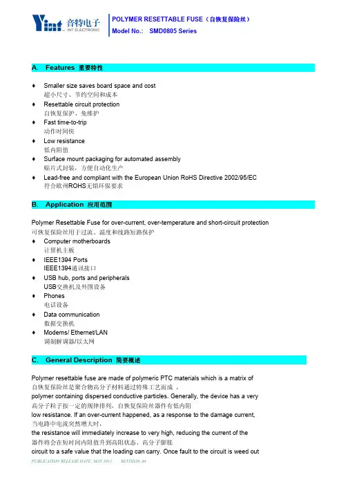
A.Features重要特性♦Smaller size saves board space and cost超小尺寸、节约空间和成本♦Resettable circuit protection自恢复保护、免维护♦Fast time-to-trip动作时间快♦Low resistance低内阻值♦Surface mount packaging for automated assembly贴片式封装,方便自动化生产♦Lead-free and compliant with the European Union RoHS Directive2002/95/EC 符合欧州ROHS无铅环保要求B.Application应用范围Polymer Resettable Fuse for over-current,over-temperature and short-circuit protection 可恢复保险丝用于过流、温度和线路短路保护♦Computer motherboards计算机主板♦IEEE1394PortsIEEE1394通讯接口♦USB hub,ports and peripheralsUSB交换机及外围设备♦Phones电话设备♦Data communication数据交换机♦Modems/Ethernet/LAN调制解调器/以太网C.General Description简要概述Polymer resettable fuse are made of polymeric PTC materials which is a matrix of自恢复保险丝是聚合物高分子材料通过特殊工艺而成,polymer containing dispersed conductive particles.Generally,the device has a very高分子粒子按一定的规律排列,自恢复保险丝器件有低内阻low resistance.If an over-current happened,as a response to the damage current,当电路中电流突然增大时,the resistance will immediately increase to very high,reducing the current of the器件将会在短时间内阻值升到高阻状态、高分子膨胀circuit to a safe value that the loading can carry.Once fault to the circuit is weed out从而起到减少过电流;and power is recuperated,the polymer will deflate itself,the device will reset and is 一旦故障排除后,高分子将会恢复正常规则排序。
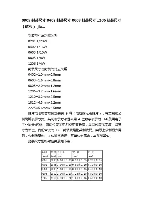
0805封装尺寸0402封装尺寸0603封装尺寸1206封装尺寸(转载)-jia...封装尺寸与功率关系:0201 1/20W0402 1/16W0603 1/10W0805 1/8W1206 1/4W封装尺寸与封装的对应关系0402=1.0mmx0.5mm0603=1.6mmx0.8mm0805=2.0mmx1.2mm1206=3.2mmx1.6mm1210=3.2mmx2.5mm1812=4.5mmx3.2mm2225=5.6mmx6.5mm贴片电阻电容常见封装有9种(电容指无级贴片),有英制和公制两种表示方式。
英制表示方法是采用4位数字表示的EIA(美国电子工业协会)代码,前两位表示电阻或电容长度,后两位表示宽度,以英寸为单位。
我们常说的0805封装就是指英制代码。
实际上公制很少用到,公制代码也由4位数字表示,其单位为毫米,与英制类似。
封装尺寸规格对应关系如下表:封装尺寸与功率有关通常如下:关于电容的封装除了上面的贴片封装外,对无极性电容,其封装模型还有RAD类型,例如“RAD-0.1”“RAD-0.2”等,后缀数字表示封装模型中两个焊盘间的距离,单位为英寸。
有极的电解电容的封装模型为RB类型,例如从“RB-.2/.4”到“RB-.5/.10”,其后缀的第一个数字表示封装模型中两个焊盘间的距离,第二个数字表示电容外形的尺寸,单位为也是英寸。
电阻:RES1,RES2,RES3,RES4;封装属性为axial系列无极性电容:cap;封装属性为RAD-0.1到rad-0.4电解电容:electroi;封装属性为rb.2/.4到rb.5/1.0电位器:pot1,pot2;封装属性为vr-1到vr-5二极管:封装属性为diode-0.4(小功率)diode-0.7(大功率)三极管:常见的封装属性为to-18(普通三极管)to-22(大功率三极管)to-3(大功率达林顿管)电源稳压块有78和79系列;78系列如7805,7812,7820等79系列有7905,7912,7920等常见的封装属性有to126h和to126v整流桥:BRIDGE1,BRIDGE2: 封装属性为D系列(D-44,D-37,D-46)电阻:AXIAL0.3-AXIAL0.7 其中0.4-0.7指电阻的长度,一般用AXIAL0.4瓷片电容:RAD0.1-RAD0.3。
自恢复保险丝选型指南自恢复保险丝是一种重要的电气保护设备,主要用于在电路发生过载或短路时切断电流,以保护电器设备和电路的安全。
选择适合的自恢复保险丝类型对确保电路的正常运行至关重要。
本文将提供一个自恢复保险丝选型指南,帮助读者了解不同类型保险丝的特点和应用场景,以便根据实际需求选择合适的保险丝。
首先,我们需要了解什么是自恢复保险丝。
自恢复保险丝,也被称为PTC保险丝(正温度系数保险丝),是一种基于正温度系数(Positive Temperature Coefficient,PTC)效应的电阻材料制成的保险丝。
当电流通过保险丝时,保险丝的温度上升,电阻值随之增加,并限制电流的流动。
一旦过载或短路情况解除,保险丝会自动恢复到正常状态,电流继续流动。
因此,自恢复保险丝不需要更换,能够提供长时间的可靠保护。
1. 电流额定值(Current Rating):根据电路中的电流需求选择适当的电流额定值。
保险丝的额定电流应略高于电路中的最大工作电流,以确保保险丝能够快速切断电流,避免电路过载损坏。
2. 额定电压值(Voltage Rating):根据电路中的电压需求选择适当的电压额定值。
保险丝的额定电压应略高于电路中的最大工作电压,以确保保险丝能够安全切断电流,并避免电弧和火灾的发生。
3.尺寸和安装方式:根据电路的空间限制和安装需求选择适当的尺寸和安装方式。
自恢复保险丝通常可分为贴片式(SMD)和插件式两种安装方式。
贴片式保险丝适合于紧凑的电路板设计,而插件式保险丝则适用于传统的插件式电路板。
4. 响应时间(Time-to-Trip):响应时间是指保险丝从开始过载或短路发生到切断电流的时间。
根据系统的要求选择适当的响应时间。
一般来说,响应时间较短的保险丝能够更快地切断电流,但也可能对电路的正常工作造成干扰。
5. 温度特性(Temperature Coefficient):不同类型的自恢复保险丝的温度特性不同。
根据环境温度和电路工作温度范围选择适当的温度特性。
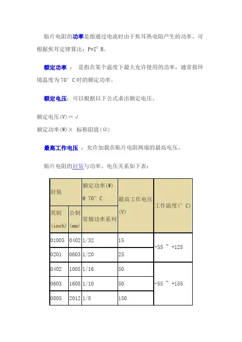
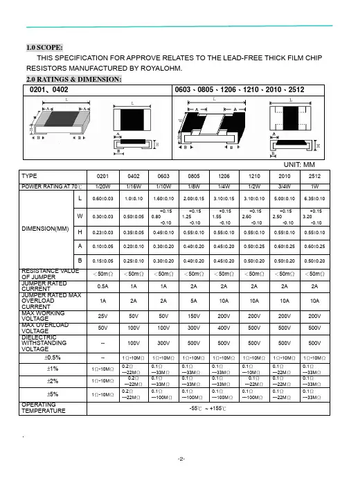
贴片电阻的功率是指通过电流时由于焦耳热电阻产生的功率。
可根据焦耳定律算出:P=I2 R。
额定功率:是指在某个温度下最大允许使用的功率,通常指环境温度为70°C时的额定功率。
额定电压:可以根据以下公式求出额定电压。
额定电压(V)=√额定功率(W)× 标称阻值(Ω)最高工作电压:允许加载在贴片电阻两端的最高电压。
贴片电阻的封装与功率、电压关系如下表:图1 (-55 ~+125)功率及环境温度降额曲线图图2 (-55 ~+155)功率及环境温度降额曲线图注意事项:•设计和使用贴片电阻时,最大功率不能超过其额定功率,否则会降低其可靠性。
•一般按额定功率的70%降额设计使用。
•也不能超过其最大工作电压,否则有击穿的危险。
•一般按最高工作电压的75%降额设计使用。
•当环境温度超过70°C,必须按照降额曲线图(图1,图2)降额使用。
我们俗称的封装是指英制。
规格书//电容规格书.pdf贴片电阻常见封装有9种,用两种尺寸代码来表示。
一种尺寸代码是由4位数字表示的EIA(美国电子工业协会)代码,前两位与后两位分别表示电阻的长与宽,以英寸为单位。
我们常说的0603封装就是指英制代码。
另一种是米制代码,也由4位数字表示,其单位为毫米。
下表列出贴片电阻封装英制和公制的关系及详细的尺寸:英制(inch ) 公制(mm)长(L)(mm)宽(W)(mm)高(t)(mm)a(mm)b(mm)02010603 0.60±0.050.30±0.050.23±0.050.10±0.050.15±0.0504021005 1.00±0.100.50±0.100.30±0.100.20±0.100.25±0.1006031608 1.60±0.150.80±0.150.40±0.100.30±0.200.30±0.2008052012 2.00±0.201.25±0.150.50±0.100.40±0.200.40±0.2012063216 3.20±0.201.60±0.150.55±0.100.50±0.200.50±0.201210 322 3.20±0. 2.50±0.0.55±0.0.50±0.0.50±0.Note:我们俗称的封装是指英制。
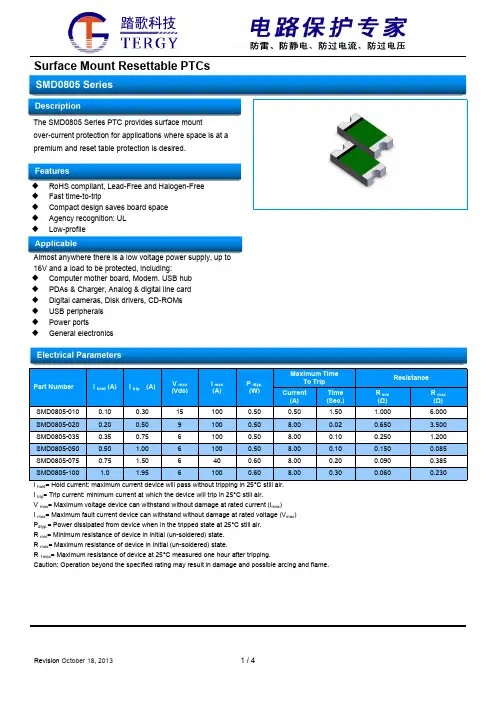
The SMD0805Series PTC provides surface mount over-current protection for applications where space is at a premium and reset table protection is desired.◆RoHS compliant,Lead-Free and Halogen-Free ◆Fast time-to-trip◆Compact design saves board space ◆Agency recognition:UL ◆Low-profileAlmost anywhere there is a low voltage power supply,up to 16V and a load to be protected,including:◆Computer mother board,B hub ◆PDAs &Charger,Analog &digital line card ◆Digital cameras,Disk drivers,CD-ROMs ◆USB peripherals ◆Power ports◆General electronicsPartNumberIhold (A)I trip (A)V max (Vdc)I max (A)P dtyp.(W)Maximum TimeTo Trip ResistanceCurrent (A)Time (Sec.)R min (Ω)R max (Ω)SMD0805-0100.100.30151000.500.50 1.50 1.000 6.000SMD0805-0200.200.5091000.508.000.020.650 3.500SMD0805-0350.350.7561000.508.000.100.250 1.200SMD0805-0500.50 1.0061000.508.000.100.1500.085SMD0805-0750.75 1.506400.608.000.200.0900.385SMD0805-1001.01.9561000.608.000.300.0600.230I hold =Hold current:maximum current device will pass without tripping in 25°C still air.I trip =Trip current:minimum current at which the device will trip in 25°C still air.V max =Maximum voltage device can withstand without damage at rated current (I max )I max =Maximum fault current device can withstand without damage at rated voltage (V max )P dtyp.=Power dissipated from device when in the tripped state at 25°C still air.R min =Minimum resistance of device in initial (un-soldered)state.R max =Maximum resistance of device in initial (un-soldered)state.R 1max =Maximum resistance of device at 25°C measured one hour after tripping.Caution:Operation beyond the specified rating may result in damage and possible arcing and flame.Part NumberAmbient Operation Temperature-40°C-20°C0°C25°C40°C 50°C 60°C 70°C 85°CHold Current (A)SMD0805-0100.140.120.110.10.80.70.60.50.3SMD0805-0200.280.250.230.200.170.140.120.100.07SMD0805-0350.470.440.390.350.300.270.240.200.14SMD0805-0500.680.620.550.500.400.370.330.290.23SMD0805-075 1.000.900.790.750.630.570.530.410.34SMD0805-1001.351.251.151.000.820.740.650.550.42A=SMD0805-010B=SMD0805-020C=SMD0805-035D=SMD0805-050E=SMD0805-075F=SMD0805-100Part MarkingXPart Identification1Example1= SMD0805-010 2= SMD0805-020 3= SMD0805-035 5= SMD0805-050 7= SMD0805-075 0= SMD0805-100Profile FeaturePb-Free Assembly Average Ramp-Up Rate (T S max to T P ) 3°C/second max. Preheat :Temperature Min (T S min) Temperature Max (T S max) Time (T S min to T S max) 150°C 200°C60-180 seconds Time maintained above: Temperature(TL) Time (tL)217°C60-150 seconds Peak/Classification Temperature(T P ): 260°C Time within 5°C of actual peak: Temperature20-40 seconds Ramp-down Rate:6°C/ second max. Time 25°C to Peak Temperature8 minutes max.Note: All temperatures refer to of the package, measured on the package body surface.Solder reflowDue to “Lead Free ” nature, Temperature and Dwelling time for the soldering zone is higher than those for Regular. This may cause damage to other components.1.Recommended max past thickness > 0.25mm.2.Devices can be cleaned using standard methods and aqueous solvent.3.Rework use standard industry practices.4.Storage Environment : < 30℃/ 60%RHCaution:1.If reflow temperatures exceed the recommended profile, devices may not meet the performance requirements.2.Devices are not designed to be wave soldered to the bottom side of the board.Soldering ParametersRamp-downPreheatCritical Zone T L to T PTime to peak temperature(t 25℃ to peak)T PT L T S(max)T S(min)25T e m p e r a t u r eRamp-upTimeA B C DeviceNominalNominal Nominal 0805 Series1.201.001.50The dimension in the table below provide the recommended pad layout for each SMD0805 devicePart Numbering Pa c k ag ingPad Layouts Unit: mmTerminal pad material Pure TinSoldering CharacteristicsMeets EIA specification RS 186-9E, ANSI/J-std-002 Category 3Material Specifications010SMD0805Product nameSMD :surface mount deviceHold Current 0.10ATape & Reel Quantity5,000 pcs/reelABCDEPart NumberMin.Max. Min. Max. Min. Max. Min. Max. Min. Max. SMD0805-010 2.00 2.20 1.20 1.50 0.50 1.00 0.20 0.60 0.10 0.45 SMD0805-020 2.00 2.20 1.20 1.50 0.45 1.00 0.20 0.60 0.10 0.45 SMD0805-035 2.00 2.20 1.20 1.50 0.45 1.00 0.20 0.60 0.10 0.45 SMD0805-050 2.00 2.20 1.20 1.50 0.30 0.60 0.20 0.60 0.10 0.45 SMD0805-075 2.00 2.20 1.20 1.50 0.40 1.00 0.20 0.60 0.10 0.45 SMD0805-1002.002.201.201.500.501.100.200.600.100.45Dimensions Unit: mmu Operation beyond the specified maximum ratings or improper use may result in damage and possible electrical arcing and/or flame.u PPTC device are intended for occasional over-current protection. Application for repeated over-current condition and/or prolonged trip are not anticipated.uAvoid contact of PPTC device with chemical solvent. Prolonged contact will damage the device performance.WarningTape and Reel SpecificationsDirection of Feed0.33 (8.4)0.512(13.0)Arbor Hole Diameter7.0 (177.8)0.212 (5.4)0.157 (4.0) 0.059(1.5)Diameter Cover tape0.314 (8.0)0.157 (4.0)Dimensions are in inches(and millimeters)。
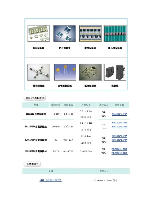
型号额定电压 额定电流外型尺寸 通过认证 资料下载2920SMD 自复保险丝15~60V0.3~3.0A7.3 ×5.0mmUL TUVPtc2920-1.PDF29 20 英寸 1812SMD 自复保险丝10~40V0.1~2.6A4.6 ×3.0mmUL TUVPTC1812-1.PDF PTC1812-2.PDF18 12 英寸 1206SMD 自复保险丝6V0.35~1.5A3.2×1.6mmUL TUV PTC1206-1.PDF PTC1206-2.PDF12 06 英寸0805SMD 自复保险丝6~15V0.1~0.75A2.0×1.2mmUL TUVPTC0805-1.PDF PTC0805-2.PDF系列外型尺寸1206 系列贴片保险丝3.2*1.6mm 0.12*0.06 英寸0603 系列贴片保险丝 1.6*0.8mm 0.06*0.03 英寸0402 系列贴片保险丝 1.0*0.5mm 0.01*0.005 英寸2410 系列贴片保险丝 6.8*2.7mm 0.24*0.10 英寸型号额定电压额定电流外型尺寸(mm)通过认证资料下载20N 速断型250V/125V 0.1∽20AΦ2.7*7.2 UL/CSA/PSE20N.pdf20T.pdf 20T 延时型250V/125V0.1∽7.0AΦ2.7*7.2 UL/CSA/PSEMCR.pdf MCR 速断型125V0.062∽10AΦ3.1*7.5UL/CSAR251 速断型125V0.062∽15AΦ2.4*7.2 UL/CSA r251-253.pdf型号额定电压额定电流外型尺寸(mm)通过认证资料下载SR5 圆柱型250V 1∽5A Φ8.4*7.6 UR/VDE/CCC SR5.pdfSS5.pdf SS5 方型250V1∽5A Φ8.6*7.6*4 UR/CCCmet.pdf MET 圆柱型250V0.04∽6.3AΦ8.4*7.6UR/VDE/CCCMST 方型250V0.04∽6.3AΦ8.6*7.6*4 UR/VDE/CCC mst.pdfU30系列自恢复保险丝 耐压 30VG16系列自恢复保险丝耐压 16VS 系列自恢复保险丝 耐压 6-16V BR 系列自恢复保险丝 耐压 125V R250系列自恢复保险丝 耐压 250V原理说明 参数说明:保持电流(Ih ):25℃静止空气环境中不触发电阻突越的最高电流。
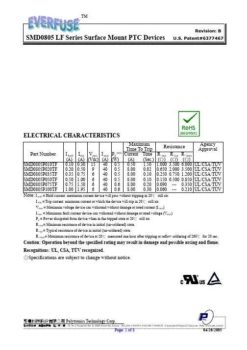
The SMD0805 Lead(Pb) Free Series, a polymer-based Positive Temperature Coefficient (PTC) device to protect electrical circuits against overcurrent conditions with resettable feature, is fully compatible with current industrial standards.The new designed SMD0805 Lead(Pb) Free Series provides surface mount overcurrent protection with superior performance that is compliant with RoHS Directive 2002/95/EC.Application: The SMD0805 Lead(Pb) Free Series is ideal for computers and peripherals and can be applied to almost anywhere there is a low voltage power supply and a load to be protected.The solder plated termination is designed to meet or exceed solderability specifications and provide excellent solder joint inspectability.Agency Approval: UL/CSA File No. E201431TÜVCertificate # R9956421 ELECTRICAL CHARACTERISTICSMaximum Time To Trip ResistanceAgency ApprovalPart NumberI hold (A)I trip (A) V max (Vdc) I max (A)P d max.(W) Current (A) Time (Sec.)R min (Ω)R typ (Ω) R 1max (Ω)SMD0805P010TF SMD0805P020TF SMD0805P035TF SMD0805P050TF SMD0805P075TF SMD0805P100TF0.100.200.350.500.751.000.30 0.50 0.75 1.00 1.50 1.95 15 9 6 6 6 64040404040400.50.50.50.50.60.60.50 8.00 8.00 8.00 8.00 8.00 1.50 0.02 0.10 0.10 0.20 0.30 1.0000.6500.2500.1500.0900.0603.500 2.000 0.750 0.500 --- --- 6.000 3.500 1.200 0.850 0.350 0.210 UL/CSA/TÜV UL/CSA/TÜV UL/CSA/TÜV UL/CSA/TÜV UL/CSA/TÜV UL/CSA/TÜV Note: I hold = Hold current: maximum current device will pass without tripping in 20℃ still air.I trip = Trip current: minimum current at which the device will trip in 20℃ still air. V max = Maximum voltage device can withstand without damage at rated current (I max ) I max = Maximum fault current device can withstand without damage at rated voltage (V max ) P d = Power dissipated from device when in the tripped state at 20℃ still air. R min = Minimum resistance of device in initial (un-soldered) state. R typ = Typical resistance of device in initial (un-soldered) state.R 1max = Maximum resistance of device at 20℃ measured one hour after tripping or reflow soldering of 260℃ for 20 sec.Caution: Operation beyond the specified rating may result in damage and possible arcing and flame. Recognitions: UL, CSA, TÜV recognized.◎Specifications are subject to change without notice.How to Select a Polymer PTC fuse:(1) Determine the following operating parameters for the circuits:(A) Normal Operating Current (I hold)(B) Maximum Circuit V oltage (V max)(C) Maximum Interrupt Current (I max)(D) Normal Operating Temperature (min℃/max℃)(2) Select the device form factor and dimension suitable for the application:Surface Mount Device (SMD Series)Radial Leaded Device (RLD Series)Axial Leaded Strap Device (STD Series)Other Custom-designed Device (Disc/Chip)(3) Compare the maximum ratings for V max and I max of the PTC device withthe circuit in application and make sure that the circuit’s requirement does not exceed the device ratings.(4) Check that the PTC device’s trip time (time-to-trip) will protect the circuit.(5) Verify that the circuit operating temperatures are within the PTC device’snormal operating temperature range.(6) Verify the performance and suitability of the chosen PTC device in theapplication.THERMAL DERATING CURVE FOR SMD0805 SERIES-40.000.0040.0080.00120.00Device Ambient Temperature ()℃0.0050.00100.00150.00200.00P e r c e n t a g e o f R a t e d C u r r e n tTHERMAL DERATING CHART FOR SMD0805 SERIES – Ihold (Amps)Ambient Operation TemperatureModel -40℃ -20℃ 0℃ 23℃40℃50℃60℃ 70℃ 85℃SMD0805P010TF 0.14 0.12 0.110.100.080.070.060.05 0.03SMD0805P020TF 0.28 0.25 0.230.200.170.140.120.10 0.07SMD0805P035TF 0.47 0.44 0.390.350.300.270.240.20 0.14SMD0805P050TF 0.68 0.62 0.550.500.400.370.330.29 0.23SMD0805P075TF 1.00 0.90 0.790.750.630.570.530.41 0.34SMD0805P100TF 1.35 1.25 1.10 1.000.820.740.650.55 0.42A VERAGE TIME-CURRENT CURVE FOR SMD0805 SERIESA:SMD0802P010TF T B:SMD0805P020TFC:SMD0805P035TF 0. D:SMD0805P050TF E:SMD0805P075TF F:SMD0805P100TF0.10 1.0010.00Fault Current (Amp.)0.01101.0010.00100.00i m e t o T r i p (S e c .)ABCDEFSOLDER REFLOWRECOMMENDED CONDITIONSCondition Reflow Peak Temp/Time 245℃≧ 5 Sec≧220℃30 Sec ~ 60 Sec Preheat 160℃~ 190℃60 Sec ~ 90 Sec Storage Condition 0℃~35℃, ≦70%RHRecommended reflow methods: IR, vapor phase oven, hot air oven, N 2 environment for lead-free Devices are not designed to be wave soldered to the bottom side of the board. Recommended maximum paste thickness is 0.25mm (0.010 inch)Devices can be cleaned using standard industry methods and solvents.Note: If reflow temperatures exceed the recommended profile, devices may not meet the performance requirements.SOLDER PAD LAYOUTS(Dimension in mm) FIGUREPHYSICAL DIMENSIONS (mm)A B CDE Part NumberMin. Max.Min. Max.Min. Max.Min. Min.Max.SMD0805P010TF 2.00 2.20 1.20 1.50 0.55 1.000.20 0.100.45 SMD0805P020TF 2.00 2.20 1.20 1.50 0.55 1.000.20 0.100.45 SMD0805P035TF 2.00 2.20 1.20 1.50 0.45 0.750.20 0.100.45 SMD0805P050TF 2.00 2.20 1.20 1.50 0.75 1.250.20 0.100.45 SMD0805P075TF 2.00 2.20 1.20 1.50 0.75 1.250.20 0.150.45 SMD0805P100TF 2.00 2.20 1.20 1.50 0.80 1.800.20 0.150.45 ENVIRONMENTAL SPECIFICATIONSOperating/StorageTemperature-40℃ to +85℃Maximum Device SurfaceTemperature in Tripped State125℃Passive Aging +85℃, 1000 hours ±5% typical resistance change Humidity Aging +85℃, 85%R.H. 1000 hours ±5% typical resistance change Thermal Shock MIL-STD-202 Method 107G+85℃/-40℃20 times -30% typical resistance changeSolvent Resistance MIL-STD-202, Method 215 No change Vibration MIL-STD-883C, Method 2007.1, Condition A No change PHYSICAL SPECIFICATIONSTerminal Material Gold-Plated Copper orSolder-Plated Copper (Solder Material: Tin(Sn) or others)Lead Solderability Meets EIA Specification RS186-9E, ANSI/J-STD-002 Category 3.Packaging 8 mm tape on 7 inch reel per EIA-481-1 (equivalent to IEC286, part 3)3000 devices per reel for P050TF5000 devices per reel for P075TFFor the others: 4000 devices per reel◎ Specifications are subject to change without notice.TAPE SPECIFICATIONS: EIA-481-1 REEL DIMENSIONS: EIA-481-1P010TF, P020TF, P035TFP050TF,P075TF, P100TFW 8.0+/-0.10 8.0+/-0.10 8.0+/-0.10 8.0+/-0.10 H 12.0+/-0.05 F 3.5+/-0.05 3.5+/-0.05 3.5+/-0.05 3.5+/-0.05 W 9.0+/-0.5 E 1 1.75+/-0.10 1.75+/-0.10 1.75+/-0.10 1.75+/-0.10 D Ø60+0.5 D 0 1.55+/-0.05 1.55+/-0.05 1.55+/-0.05 1.55+/-0.05F Ø13.0+/-0.2 D 1 1.0 (min)1.0 (min)1.0 (min)1.0 (min)C Ø178+/-1.0 P 0 4.0+/-0.10 4.0+/-0.10 4.0+/-0.10 4.0+/-0.10 H 1 11+/-0.5 P 1 4.0+/-0.10 4.0+/-0.10 4.0+/-0.10 4.0+/-0.10 W 1 2.2+/-0.5 P 2 2.0+/-0.05 2.0+/-0.05 2.0+/-0.05 2.0+/-0.05 W 2 3.0+0.5 A 0 1.45+/-0.10 1.42+/-0.10 1.65+/-0.10 1.65+/-0.10 W 3 4.0+0.5 B 0 2.30+/-0.10 2.24+/-0.10 2.35+/-0.10 2.35+/-0.10 W 4 5.5+0.5T 0.25+/-0.10 0.20+/-0.10 0.20+/-0.10 0.25+/-0.10 (mm)K 0 0.74+/-0.10 1.04+/-0.10 1.05+/-0.10 1.50+/-0.10 Leader min . 390 390 390 390 Trailer min.160 160 160 160(mm)PART NUMBERING SYSTEMSMD0805 P □□□TFF: Lead-freeVersionMultilayerThicknessCurrent RatingPolytronics Symbolinch) Device1/100Length/Width(Unit:Dimensions:Surface Mount Device。
贴片自恢复保险丝SCF0805系列型号
硕凯电子(Sylvia)
一、产品图
二、产品描述
贴片自恢复保险丝(PPTC:高分子自恢复保险丝)是一种正温度系数聚合物热敏电阻,作过流保护用,可代替电流保险丝。
电路正常工作时它的阻值很小(压降很小),当电路出现过流使它温度升高时,阻值急剧增大几个数量级,使电路中的电流减小到安全值以下,从而使后面的电路得到保护,过流消失后自动恢复为低阻值。
其效果与开关元件类似,只是响应速度较慢。
三、产品型号
SCF010-0805R,SCF020-0805R,SCF035-0805R,SCF050-0805R,SCF050-9-0805R,SCF075-0805R,SCF100-0805R。
四、相关曲线图
五、产品特性
1、符合RoHS标准,无铅和无卤素
2、动作时间快
3、设计紧凑,节省电路板空间
4、低电阻
5、半高
六、产品应用
1、PC主板的即插即用的保护
2、手机电池和端口保护
3、游戏控制台端口保护
4、USB外围设备
5、磁盘驱动器
6、掌上电脑/数码相机
7、电源端口
8、通用电子。
0805封装尺寸/0402封装尺寸/0603封装尺寸/1206封装尺寸(转载)电子元器件2010-09-08 21:21:48 阅读672 评论0 字号:大中小订阅封装尺寸与功率关系:0201 1/20W0402 1/16W0603 1/10W0805 1/8W1206 1/4W封装尺寸与封装的对应关系0402=1.0mmx0.5mm0603=1.6mmx0.8mm0805=2.0mmx1.2mm1206=3.2mmx1.6mm1210=3.2mmx2.5mm1812=4.5mmx3.2mm2225=5.6mmx6.5mm贴片电阻电容常见封装有9种(电容指无级贴片),有英制和公制两种表示方式。
英制表示方法是采用4位数字表示的EIA(美国电子工业协会)代码,前两位表示电阻或电容长度,后两位表示宽度,以英寸为单位。
我们常说的0805封装就是指英制代码。
实际上公制很少用到,公制代码也由4位数字表示,其单位为毫米,与英制类似。
封装尺寸规格对应关系如下表:封装尺寸与功率有关通常如下:关于电容的封装除了上面的贴片封装外,对无极性电容,其封装模型还有RAD类型,例如“RAD-0.1”“RAD-0.2”等,后缀数字表示封装模型中两个焊盘间的距离,单位为英寸。
有极的电解电容的封装模型为RB类型,例如从“RB-.2/.4”到“RB-.5/.10”,其后缀的第一个数字表示封装模型中两个焊盘间的距离,第二个数字表示电容外形的尺寸,单位为也是英寸。
电阻:RES1,RES2,RES3,RES4;封装属性为axial系列无极性电容:cap;封装属性为RAD-0.1到rad-0.4电解电容:electroi;封装属性为rb.2/.4到rb.5/1.0电位器:pot1,pot2;封装属性为vr-1到vr-5二极管:封装属性为diode-0.4(小功率)diode-0.7(大功率)三极管:常见的封装属性为to-18(普通三极管)to-22(大功率三极管)to-3(大功率达林顿管)电源稳压块有78和79系列;78系列如7805,7812,7820等79系列有7905,7912,7920等常见的封装属性有to126h和to126v整流桥:BRIDGE1,BRIDGE2: 封装属性为D系列(D-44,D-37,D-46)电阻:AXIAL0.3-AXIAL0.7其中0.4-0.7指电阻的长度,一般用AXIAL0.4瓷片电容:RAD0.1-RAD0.3。
C ustomer:·Technical Data Sheet PN:XGS-PB2012UB-02 For:IF=20mAContents1.Features2.Applications3.Package dimensions4.Absolute maximum rating5.Electrical optical characteristics6.BIN range7.Package label8.Soldering pad dimensions9.Soldering conditions10.Package tape specifications11.T ypical electro-optical characteristics curves12.Reliability test items and conditions13.Cautions14.Note◆F eatures:Compatible with automatic placement equipmentCompatible with reflow solder processLow power consumption and wide viewing angleThis product doesn’t contain restriction Substance, comply ROHS standard.◆A pplications:Automotive and TelecommunicationFlat backlight for LCD ,switch and symbol in telephone and faxGeneral use for indicators◆P ackage Dimensions:Unit:mmTolerenc e±0.1Electrodes: Ag Plating◆A bsolute Maximum Rating (Ta=25℃)* I FP condition: pulse width ≤1ms ,duty cycle ≤1/10◆E lectrical Optical Characteristics(Ta=25℃)Notes: 1.Tolerance of Luminous Intensity ±10%2.Tolerance of Dominant Wavelength ±2nm3.Tolerance of Forward Voltage ±0.05V4.Luminous Intensity is measured by XGSLED’s equipment on bare chips◆ Soldering Pad Dimensions:◆ S oldering Conditions (Maximum allowable soldering conditions)Reflow soldering profile<Pb-free solder>Time• Reflow soldering should not be done more than two times. • Do not stress its resin while soldering.• After soldering,do not warp the circuit board.T e m p e r a t u r e◆ P ackage Tape Specifications: (3000 pcs/Reel)Reel Lead Min.60mm No LEDs5 Reels in one Box10 Boxes in one Carton◆ T ypical Electro-Optical Characteristics Curves :Forward Current Vs Ambient Temperature5040302010100250Forward Current Vs Relative Luminosity204060801001020304050Ambient Temperature Ta (° C)Forward Current (mA)200 15010050 Relative Luminosity VsAmbient TemperatureIf=15mA-50° -60°-70°-80°-90°-40°-30°-20°-10°0°10°20°30°40°50°60°70°80°90° 0 0204060801001.00.50.5Radiation Angle1.0Ambient Temperature Ta (° C)R e l a t i v e L u m i n o s i t y (%)F o r w a r d C u r r e n t (m A )R e l a t i v e L u m i n o s i t y (%)◆Reliability(1)Test Items and Conditions(2)C riteria of judging the damage◆C autions1、PackageWhen moisture is absorbed into the package it may vaporize and expand during soldering. There is apossibility that this can cause exfoliation of the contacts and damage to the optical characteristics of the LEDs. So the moisture proof package is used to keep moisture to a minimum in the package.2、StorageBefore opening the package: The LEDs should be kept at 5~30°C and 60%RH or less. The LEDs should be used within a year.After opening the package: The LED must be used within 24 hours, else should be kept at 5~30℃and 30% RH or less. The LEDs should be used within 7days after opening the package. If unused LEDs remain, they should be stored in moisture proof packages, recommended to return the LEDs to the original moisture proof bag and to reseal the moisture proof bag again.If the LEDs have exceeded the storage time, baking treatment should be performed more than 24hours at 60±5°C.3、Soldering IronEach terminal is to the tip of soldering iron temperature less than 300℃ for 3 seconds within once inless than the soldering iron capacity 25 W.Leave two seconds and more internals, and do soldering of each terminal. Be careful because the damage of the product is often started at the time of the hand solder.4、RepairingRepairing should not be done after the LEDs have been soldered. When repairing is unavoidable, a double-head soldering iron should be used (as below figure). It should be confirmed beforehand whether the characteristics of the LEDs will or will not be damaged by repairing.5、The LED electrode sections are comprised of a gold plated. The gold surface may be affected by environments which contain corrosive gases and so on. Please avoid conditions which may cause the LED to corrode or discolor. This corrosion or discoloration may cause difficulty during soldering operations. It is recommended that the User use the LEDs as soon as possible.6、Please avoid rapid transitions in ambient temperature, especially in high humidity environments where condensation can occur.◆Notes:1、Above specification may be changed without notice. We will reserve authority on material change for above specification.2 、When using this product, please observe the absolute maximum ratings and the instructions for the specification sheets. We assume no responsibility for any damage resulting from use of the product which does not comply with the instructions included in the specification sheets.。
贴片自恢复保险丝测试指南一:测试流程如下:1. 初始内阻Rimin 测量:拆包装,拿出保险丝,测量保险丝的内阻;2. 焊接:将保险丝通过回流焊焊接在PCB上,PCB上连接有引线,便于进行电性能测试(如上图所示);3. 保持电流Ihold测试:选用直流恒压恒流源进行测试。
将电压调节到规格书规定的电压Vmax,电流调节到规格书规定的保持电流Ihold,通电15分钟;4. 动作电流Itrip测试:选用直流恒压恒流源进行测试。
将电压调节到规格书规定的电压Vmax,电流调节到规格书规定的保持电流Itrip,通电5分钟;5. R1max测试:将动作后的保险丝放置冷却1小时,测量保险丝的内阻。
二:测试标准:1. 测试环境为25℃的室温环境,无光照、无热辐射;2. 保险丝初始内阻Rimin 需在规格书范围内;3. 保险丝在Ihold电流下保持15分钟不动作,判定为合格;4. 保险丝在Itrip电流下5分钟以内动作,判定为合格;5. 保险丝动作后内阻R1max需在规格书范围内。
三:测试过程中的常见问题附FAQ:Q:实验室只有万用表,可以对内阻进行测量吗?A:推荐使用专业的微电阻测试仪表(如Hioki 3540)进行测量,在没有微阻计的情况下可用万用表作粗略的测量。
Q:实验室没有专业电源设备,用普通的恒压恒流源进行测试可以吗?A:可以用普通的恒压恒流源进行测试。
Q:实验室没有PCB,可以直接放在桌面上进行测试吗?A:保险丝能不能起保护,本质上是保险丝吸收的热量大于释放的热量,保险丝本身的热量不断积累,达到一定程度后保险丝即会起保护。
使用PCB进行测试是对保险丝使用环境的真实摸拟。
若在木质桌面、塑料板、或毛布上面进行测试,因为不同材质的热交换不同,会影响到保险丝热量的释放,从而影响到测试的准确性。
Q:实验室没有SMT设备,可以进行手工焊接吗?A:高分子是自恢复保险丝主要的材料之一。
因高分子受热会影响到其微观状态,进而影响到保险丝的内阻。
(a) RoHS Compliant & Halogen Free
(b) Applications: All high-density boards
(c) Product Features: Small surface mountable, Solid state, Faster time to trip than
standard SMD devices, Lower resistance than standard SMD devices (d) Operation Current: 0.10A~1.10A (e) Maximum Voltage: 6V~24V DC
(f) Temperature Range : -40℃ to 85℃
2. Agency Recognition
UL : File No. E211981TÜV: File No. R50090556
3. Electrical Characteristics (23℃)
H I T =Trip current-minimum current at which the device will always trip at 23℃ still air. V MAX =Maximum voltage device can withstand without damage at it rated current.(I MAX )
I MAX = Maximum fault current device can withstand without damage at rated voltage (V MAX ).
Pd=Typical power dissipated-type amount of power dissipated by the device when in the tripped state in 23℃ still air environment. R MIN =Minimum device resistance at 23℃ prior to tripping.
R 1MAX =Maximum device resistance at 23℃ measured 1 hour after tripping or reflow soldering of 260℃ for 20 seconds. Termination pad characteristics
Termination pad materials: Pure Tin
4.
FSMD Product Dimensions (Millimeters)
6. Typical Time-To-Trip at 23℃
T
i
m e -t o -t r i p (S )
7. Material Specification
Terminal pad material: Pure Tin
Soldering characteristics: Meets EIA specification RS 186-9E, ANSI/J-std-002 Category 3
8. Part Numbering and Marking System
Part Numbering System Part Marking System
S M D □ □ □ - □ □ - 0805 F □
Warning: electrical arcing and/or flame.
-PPTC device are intended for occasional overcurrent protection. Application for repeated overcurrent condition and/or prolonged trip are not anticipated. 甲、 -Avoid contact of PPTC device with chemical solvent. Prolonged contact will damage the device
performance. A = SMD010-0805 / SMD010-24-0805 B = SMD020-0805 C = SMD035-0805 D = SMD050-0805 / SMD050-9-0805 E = SMD075-0805 F = SMD100-0805 G= SMD110-0805
Current Rating Part Identification Logo Example Voltage Rating
9. Pad Layouts 、Solder Reflow and Rework Recommendations
The dimension in the table below provide the recommended pad layout for each SMD 0805 device
Note 1: All temperatures refer to of the package,
measured on the package body surface.
Reflow Profile。