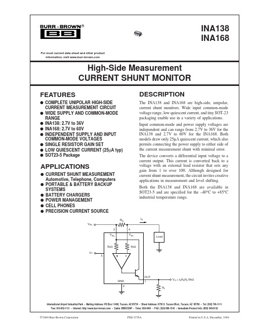
INA168
- 格式:pdf
- 大小:72.25 KB
- 文档页数:7
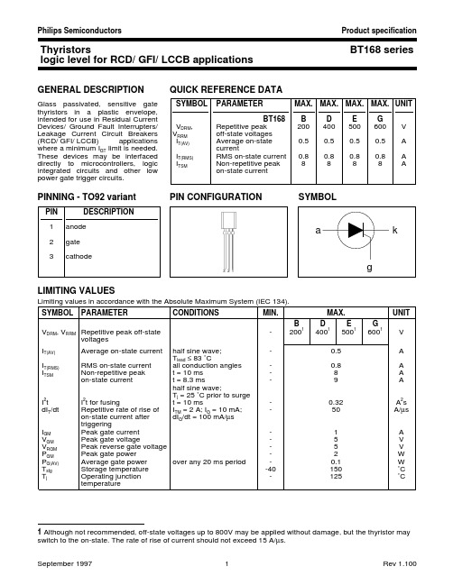
GENERAL DESCRIPTIONQUICK REFERENCE DATAGlass passivated,sensitive gate SYMBOL PARAMETER MAX.MAX.MAX.MAX.UNIT thyristors in a plastic envelope,intended for use in Residual Current BT168B D E G Devices/Ground Fault Interrupters/V DRM ,Repetitive peak 200400500600V Leakage Current Circuit Breakers V RRM off-state voltages (RCD/ GFI/ LCCB)applications I T(AV)Average on-state 0.50.50.50.5A where a minimum I GT limit is needed.currentThese devices may be interfaced I T(RMS)RMS on-state current 0.80.80.80.8A directly to microcontrollers,logic I TSMNon-repetitive peak 8888Aintegrated circuits and other low on-state currentpower gate trigger circuits.PINNING - TO92 variantPIN CONFIGURATION SYMBOLLIMITING VALUESLimiting values in accordance with the Absolute Maximum System (IEC 134).SYMBOLPARAMETERCONDITIONSMIN.MAX.UNIT B D E G V DRM , V RRM Repetitive peak off-state-2001400150016001V voltages I T(AV)Average on-state current half sine wave;-0.5A T lead ≤ 83 ˚CI T(RMS)RMS on-state current all conduction angles -0.8A I TSMNon-repetitive peak t = 10 ms -8A on-state currentt = 8.3 ms-9A half sine wave;T j = 25 ˚C prior to surge I 2t I 2t for fusingt = 10 ms-0.32A 2s dI T /dt Repetitive rate of rise of I TM = 2 A; I G = 10 mA;-50A/µs on-state current after dI G /dt = 100 mA/µstriggeringI GM Peak gate current -1A V GM Peak gate voltage-5V V RGM Peak reverse gate voltage -5V P GM Peak gate power -2W P G(AV)Average gate power over any 20 ms period -0.1W T stg Storage temperature -40150˚C T jOperating junction -125˚Ctemperature1 Although not recommended, off-state voltages up to 800V may be applied without damage, but the thyristor may switch to the on-state. The rate of rise of current should not exceed 15 A/µs.THERMAL RESISTANCESSYMBOL PARAMETER CONDITIONSMIN.TYP.MAX.UNIT R th j-lead Thermal resistance --60K/W junction to lead R th j-aThermal resistance pcb mounted; lead length = 4mm -150-K/Wjunction to ambientSTATIC CHARACTERISTICST j = 25 ˚C unless otherwise stated SYMBOL PARAMETER CONDITIONSMIN.TYP.MAX.UNIT I GT Gate trigger current V D = 12 V; I T = 10 mA; gate open circuit 2050200µA I L Latching current V D = 12 V; I GT = 0.5 mA; R GK = 1 k Ω-26mA I H Holding current V D = 12 V; I GT = 0.5 mA; R GK = 1 k Ω-25mA V T On-state voltage I T = 1 A- 1.2 1.35V V GT Gate trigger voltage V D = 12 V; I T = 10 mA; gate open circuit -0.50.8V V D = V DRM(max); I T = 10 mA; T j = 125 ˚C;0.20.3-V gate open circuitI D , I ROff-state leakage currentV D = V DRM(max); V R = V RRM(max); T j = 125 ˚C;-0.050.1mAR GK = 1 k ΩDYNAMIC CHARACTERISTICST j = 25 ˚C unless otherwise stated SYMBOL PARAMETER CONDITIONSMIN.TYP.MAX.UNIT dV D /dt Critical rate of rise of V DM = 67% V DRM(max); T j = 125 ˚C;-25-V/µs off-state voltageexponential waveform; R GK = 1 k Ωt gt Gate controlled turn-on I TM = 2 A; V D = V DRM(max); I G = 10 mA;-2-µs timedI G /dt = 0.1 A/µst qCircuit commutated V D = 67% V DRM(max); T j = 125 ˚C;-100-µsturn-off timeI TM = 1.6 A; V R = 35 V; dI TM /dt = 30 A/µs;dV D /dt = 2 V/µs; R GK = 1 k ΩMECHANICAL DATANotes1. Epoxy meets UL94 V0 at 1/8".DEFINITIONSData sheet statusObjective specification This data sheet contains target or goal specifications for product development. Preliminary specification This data sheet contains preliminary data; supplementary data may be published later. Product specification This data sheet contains final product specifications.Limiting valuesLimiting values are given in accordance with the Absolute Maximum Rating System (IEC 134). Stress above one or more of the limiting values may cause permanent damage to the device. These are stress ratings only and operation of the device at these or at any other conditions above those given in the Characteristics sections of this specification is not implied. Exposure to limiting values for extended periods may affect device reliability. Application informationWhere application information is given, it is advisory and does not form part of the specification.© Philips Electronics N.V. 1997All rights are reserved. Reproduction in whole or in part is prohibited without the prior written consent of the copyright owner.The information presented in this document does not form part of any quotation or contract, it is believed to be accurate and reliable and may be changed without notice. No liability will be accepted by the publisher for any consequence of its use. Publication thereof does not convey nor imply any license under patent or other industrial or intellectual property rights.LIFE SUPPORT APPLICATIONSThese products are not designed for use in life support appliances, devices or systems where malfunction of these products can be reasonably expected to result in personal injury. Philips customers using or selling these products for use in such applications do so at their own risk and agree to fully indemnify Philips for any damages resulting from such improper use or sale.。

1dc2708afDESCRIPTIONLTC7001Fast High VoltageHigh Side NMOS Static Switch DriverDemonstration circuit 2708A is a 135V, high side switch featuring the LTC ®7001. The demo board is designed to switch a 5A output load from 0V up to 135V. This board offers a low 50ns (typical) propagation delay, fast switching times (<10ns) and 100% duty cycle operation.The LTC7001 is a fast high voltage high side N-channel MOSFET driver . An internal charge pump fully enhances an external N-channel MOSF ET switch, allowing it to remain on indefinitely. A powerful gate driver can drive large gate capacitance MOSFETs with very short transition times, ideal for both high frequency switching and static switch applications. The LTC7001 operates over a 0V to 135V input supply range.The demo board includes input capacitors and an output diode to accommodate input and output supply induc-tance when switching loads. The switch can be controlled by providing an external signal on INPUT turret. The V CCL , L T , L TC, L TM, Linear Technology and the Linear logo are registered trademarks of Analog Devices, Inc. All other trademarks are the property of their respective owners.PERFORMANCE SUMMARYinput must be powered with an external power supply to provide power to the controller . Positions for RC delay network to control inrush current are also included.The LTC7001 data sheet gives a complete description of the part, operation and application information. The data sheet must be read in conjunction with this demo manual for demo circuit 2708A. Proper board layout is essential for maximum thermal and electrical performance. See the data sheet sections for details. The LTC7001 is available in 10-lead MSOP package and three operating junction temperature grades, extended and industrial from –40°C to 125°C, a high temp automotive version from –40°C to 150°C and a military grade version from –55°C to 150°C.Design files for this circuit board are available at http://www.linear .com/demo/DC2708ASpecifications are at T A = 25°CSYMBOL PARAMETER CONDITIONSMIN TYPMAX UNITSV IN Input Voltage 0135V I OUT Output Current 5A Insertion Drop V IN – V OUT , 5A Load, Input to Output Terminals115mV V CC Main Supply712V V CCUVV CC Undervoltage Lockout V CC Rising V CC Falling Hysteresis 6.5 5.87.0 6.4 0.67.5 6.9V V V Input to Output Propagation Delay V IN = 135V, 50Ω Load, INP = 2.2V to V OUT = 13.5V 50ns Output Rise TimeV IN = 135V, 50Ω Load, 10% to 90%6.5ns2dc2708afdirectly across the output capacitor as shown in Figure 2.1. With input power supply set to zero volt and power off, 2. 3. Set V CC V CC supply to V CC and GND.6. Connect a signal source across INPUT and GND. Apply a signal with 2.2V or higher will turn-on the high side switch.7. Check for the proper output voltage using a voltmeter. Output voltage should be close to input voltage.8. Once the proper output voltage is established, adjust the load.Figure 1. Proper Measurement Equipment SetupI SIGNALSOURCE3dc2708afQUICK START PROCEDURETYPICAL PERFORMANCE CHARATERISTICSFigure 2. Measuring Output Voltage During Switching across C5. Note that C5 May Not Be InstalledFigure 3. Rise Time into 50Ω Load (V IN = 135V, CH2 V INP 5V/DIV , CH3 V OUT 50V/DIV , 10ns/DIV)Figure 4. Board PhotoCHANNEL 2: INP CHANNEL 3: V OUT50Ω RESISTIVE LOADPARTS LISTITEM QTY REFERENCE PART DESCRIPTION MANUFACTURER/PART NUMBER Required Circuit Components13C2, C3, C4CAP., 1μF, X7T, 250V, 1812TDK, C4532X7T2E105K250KA21C7CAP., 0.1μF, X7R, 25V, 10%, 0805AVX, 08053C104KAT2A31C8CAP., 1μF, X7R, 25V,10%, 0805AVX, 08053C105KAT2A41D1DIODE, ES1PD, 200V, 1A, DO-220AA VISHAY, ES1PD-M3/84A51Q1MOSFET, N-CH, 150V, POWERPAK-SO-8FAIRCHILD, FDMS8625061R3RES., 10Ω, 1/10W, 1%, 0603VISHAY, CRCW060310R0FKEA71R4RES., 0Ω, 1/10W, 0805VISHAY CRCW08050000Z0EA81U1IC, LTC7001EMSE, MSE-10LINEAR TECH., LTC7001EMSE#PBF Additional Demo Board Circuit Components11C1CAP., 22μF, ALUM, 160V, 20%,10mm × 12.5mm SUN ELECT., 160ME22HPC20C5CAP., OPTIONAL, 1812OPTIONAL30C6CAP., OPTIONAL, 0603OPTIONAL40C9CAP., OPTIONAL, 1206OPTIONAL50D2DIODE OPTIONAL, POWERDI5OPTIONAL61D3DIODE, OPTIONAL, SOT23OPTIONAL70D4DIODE, OPTIONAL, SOT23OPTIONAL80Q2MOSFET, OPTIONAL, D2-PAK OPTIONAL90Q3MOSFET, OPTIONAL, POWERPAK-SO-8OPTIONAL101R1RES., SENSE, 0Ω, 1/2W, 1%, 1225TEPRO, RN5326110R2, R9RES., OPTIONAL, 0805OPTIONAL123R5, R6, R7RES., 0Ω, 1/10W, 0603VISHAY CRCW06030000Z0EA130R8, R10, R11, R12RES., OPTIONAL, 0603OPTIONALHardware: For Demo Board Only17E1–E7TESTPOINT, TURRET 0.094"MILL MAX 2501-2-00-80-00-00-07-0 24MTGS. @ 4 CORNERS STAND-OFF, NYLON 0.559" TALL WURTH ELEKTRONIK, 702935500 31PCB, DC2708A DEMO CIRCUIT 2708A4dc2708af5dc2708afInformation furnished by Linear Technology Corporation is believed to be accurate and reliable. However , no responsibility is assumed for its use. Linear Technology Corporation makes no representa-tion that the interconnection of its circuits as described herein will not infringe on existing patent rights.SCHEMATIC DIAGRAMDEMONSTRATION BOARD IMPORTANT NOTICELinear Technology Corporation (LTC) provides the enclosed product(s) under the following AS IS conditions:This demonstration board (DEMO BOARD) kit being sold or provided by Linear Technology is intended for use for ENGINEERING DEVELOPMENT OR EVALUATION PURPOSES ONLY and is not provided by LTC for commercial use. As such, the DEMO BOARD herein may not be complete in terms of required design-, marketing-, and/or manufacturing-related protective considerations, including but not limited to product safety measures typically found in finished commercial goods. As a prototype, this product does not fall within the scope of the European Union directive on electromagnetic compatibility and therefore may or may not meet the technical requirements of the directive, or other regulations. If this evaluation kit does not meet the specifications recited in the DEMO BOARD manual the kit may be returned within 30 days from the date of delivery for a full refund. THE FOREGOING WARRANTY IS THE EXCLUSIVE WARRANTY MADE BY THE SELLER TO BUYER AND IS IN LIEU OF ALL OTHER WARRANTIES, EXPRESSED, IMPLIED, OR STATUTORY, INCLUDING ANY WARRANTY OF MERCHANTABILITY OR FITNESS FOR ANY PARTICULAR PURPOSE. EXCEPT TO THE EXTENT OF THIS INDEMNITY, NEITHER PARTY SHALL BE LIABLE TO THE OTHER FOR ANY INDIRECT, SPECIAL, INCIDENTAL, OR CONSEQUENTIAL DAMAGES.The user assumes all responsibility and liability for proper and safe handling of the goods. Further, the user releases LTC from all claims arising from the handling or use of the goods. Due to the open construction of the product, it is the user’s responsibility to take any and all appropriate precautions with regard to electrostatic discharge. Also be aware that the products herein may not be regulatory compliant or agency certified (FCC, UL, CE, etc.).No License is granted under any patent right or other intellectual property whatsoever. LTC assumes no liability for applications assistance, customer product design, software performance, or infringement of patents or any other intellectual property rights of any kind.LTC currently services a variety of customers for products around the world, and therefore this transaction is not exclusive.Please read the DEMO BOARD manual prior to handling the product. Persons handling this product must have electronics training and observe good laboratory practice standards. Common sense is encouraged.This notice contains important safety information about temperatures and voltages. For further safety concerns, please contact a LTC application engineer.Mailing Address:Linear Technology1630 McCarthy Blvd.Milpitas, CA 95035Copyright © 2004, Linear Technology Corporation。
Low Noise, CascadableSilicon Bipolar MMIC Amplifier Technical DataFeatures•Cascadable 50 Ω Gain Block • 3 dB Bandwidth:DC to 1.8 GHz•26 dB Typical Gain at1.5␣GHz•10 dBm Typical P1dB at1.5␣GHz•Unconditionally Stable (k>1)•Surface Mount PlasticPackage INA-1038686 Plastic PackageTypical Biasing ConfigurationVCCRF IN RF OUTDescriptionThe INA-10386 is a low-noise silicon bipolar Monolithic Micro-wave Integrated Circuit (MMIC)feedback amplifier housed in a low cost surface mount plastic package. It is designed for narrow or wide bandwidth commercial and industrial applications that require high gain and moderate power.The INA series of MMICs is fabricated using HP’s 10 GHz f T, 25␣GHz f MAX, ISOSAT™-I silicon bipolar process which uses nitride self-alignment, submicrometer lithography, trench isolation, ion implantation, gold metallization and polyimide intermetal dielec-tric and scratch protection to achieve excellent performance, uniformity and reliability.INA-10386 Absolute Maximum RatingsParameterAbsolute Maximum [1]Device Current80 mA Power Dissipation [2,3]750 mW RF Input Power+13 dBm Junction Temperature 150°C Storage Temperature–65 to 150°CThermal Resistance:θjc = 100°C/WNotes:1.Permanent damage may occur if any of these limits are exceeded.2.T CASE = 25°C.3.Derate at 10 mW/°C for T C > 75°C.INA-10386 Part Number Ordering InformationPart Number No. of DevicesContainer INA-10386-TR110007" Reel INA-10386-BLK100Antistatic BagG P Power Gain (|S 21|2) f = 1.5 GHz dB 23.026.0∆G P Gain Flatness f = 0.1 to 1.5 GHzdB ±1.0f 3 dB 3 dB Bandwidth [2]GHz 1.8I SO Reverse I solation (|S 12|2) f = 2.0 GHz dB30I nput VSWR f = 0.1 to 2.0 GHz 1.5:1Output VSWR f = 0.1 to 2.0 GHz 1.5:1NF 50 Ω Noise Figuref = 1.5 GHz dB 3.8P 1 dB Output Power at 1 dB Gain Compression f = 1.5 GHz dBm 10IP 3Third Order Intercept Point f = 1.5 GHz dBm 23t D Group Delay f = 1.5 GHz psec 250I d Device CurrentmA 354555dV/dTDevice Voltage Temperature CoefficientmV/°C+10Notes:1.The recommended operating current range for this device is 40 to 60 mA. Typical performance as a function of current is on the following page.INA-10386 Electrical Specifications [1], T A = 25°CSymbolParameters and Test Conditions: V d = 6V, Z O = 50 ΩUnitsMin.Typ.Max.VSWRINA-10386 Typical Scattering Parameters (Z O = 50 Ω, T A = 25°C, V d = 6 V)Freq.GHzMagAngdBMagAngdBMagAngMagAngk0.05.12–926.621.4–4–35.2.0171.11–3 1.510.10.11–1726.721.6–8–35.6.0173.12–10 1.500.50.13–7926.721.6–38–35.7.01610.07–40 1.591.00.17–13726.821.9–80–34.1.02043.0318 1.331.50.2117126.020.0–126–33.1.02353.0732 1.262.00.2112723.615.1–168–29.9.03255.079 1.232.50.1910621.712.2159–28.4.03858.0442 1.273.00.148619.29.1127–26.7.04855.0556 1.373.50.078516.8 6.997–24.8.05850.0647 1.444.00.0814814.2 5.170–24.7.05851.0440 1.82S 11S 21S 12 S 22INA-10386 Typical Performance, T A = 25°C(unless otherwise noted)FREQUENCY (GHz)FREQUENCY (GHz)Figure 5. Output Power at 1 dB Gain Compression vs. Frequency.Figure 6. Noise Figure vs. Frequency.2.03.05.04.0252627N F (d B )G p (d B )TEMPERATURE (°C)Figure 4. Output Power and 1 dB Gain Compression, NF and Power Gain vs. CaseTemperature, f = 1.5 GHz, V d = 6 V.1015202530G p (d B )86 Plastic Package Dimensions0.51 ±。
ATmega168 简介ATmega168是基于增强的A VR RISC结构的低功耗8 位CMOS微控制器。
由于其先进的指令集以及单时钟周期指令执行时间,ATmega168 的数据吞吐率高达 1 MIPS/MHz,从而可以缓减系统在功耗和处理速度之间的矛盾。
ATmega168 A VR 内核具有丰富的指令集和32 个通用工作寄存器。
所有的寄存器都直接与算逻单元(ALU) 相连接,使得一条指令可以在一个时钟周期内同时访问两个独立的寄存器。
这种结构大大提高了代码效率,并且具有比普通的CISC 微控制器最高至10 倍的数据吞吐率。
ATmega168 有如下特点:16K字节的系统内可编程Flash(具有同时读写的能力,即RWW),512 字节EEPROM,1K 字节SRAM,23 个通用I/O 口线,32 个通用工作寄存器,用于边界扫描的DebuyWIRE接口,支持片内调试与编程,三个具有比较模式的灵活的定时器/ 计数器(T/C),片内/外中断,可编程串行USART,有起始条件检测器的通用串行接口,8路10位具有可选差分输入级可编程增益(TQFP 封装) 的ADC ,具有片内振荡器的可编程看门狗定时器,一个SPI 串行端口,以及五个可以通过软件进行选择的省电模式。
工作于空闲模式时CPU 停止工作,而USART、两线接口、A/D 转换器、SRAM、T/C、SPI 端口以及中断系统继续工作;掉电模式时晶体振荡器停止振荡,所有功能除了中断和硬件复位之外都停止工作;在省电模式下,异步定时器继续运行,允许用户保持一个时间基准,而其余功能模块处于休眠状态;ADC 噪声抑制模式时终止CPU 和除了异步定时器与ADC 以外所有I/O 模块的工作,以降低ADC 转换时的开关噪声;Standby 模式下只有晶体或谐振振荡器运行,其余功能模块处于休眠状态,使得器件只消耗极少的电流,同时具有快速启动能力;扩展Standby 模式下则允许振荡器和异步定时器继续工作。