HX3141 DC-DC升压IC
- 格式:pdf
- 大小:262.92 KB
- 文档页数:7
基本指南進階指南相機的基本操作自動模式/混合自動拍攝模式其他拍攝模式播放模式無線功能設定選單配件附錄索引P 模式Tv 、Av 、M 、C1及C2模式用前須知基本指南進階指南相機的基本操作自動模式/混合自動拍攝模式其他拍攝模式播放模式無線功能設定選單配件附錄索引P 模式Tv 、Av 、M 、C1及C2模式用前須知基本指南進階指南相機的基本操作自動模式/混合自動拍攝模式其他拍攝模式播放模式無線功能設定選單配件附錄索引P 模式Tv 、Av 、M 、C1及C2模式用前須知基本指南進階指南相機的基本操作自動模式/混合自動拍攝模式其他拍攝模式播放模式無線功能設定選單配件附錄索引P 模式Tv 、Av 、M 、C1及C2模式用前須知2223232424262728293131 (33)34 (37) (37)37基本指南進階指南相機的基本操作自動模式/混合自動拍攝模式其他拍攝模式播放模式無線功能設定選單配件附錄索引P 模式Tv 、Av 、M 、C1及C2模式用前須知5353 (53)5556) (56)) (57)5858) (58)) (59)) (59)) (59)) (60)(以1分鐘的短片為例) (60)) (61)61 (62)63636464656566) (66)在混合自動拍攝模式下拍攝 .播放短片摘要靜止影像/短片靜止影像短片場景圖示 .螢幕上的方框 ......................................................................................常用的便捷功能 ...............................................................................42使用自拍 ..............................................................................................使用自拍功能以避免相機震動 .....................................................自訂自拍 .........................................................................................輕觸螢幕進行拍攝(輕觸式快門) .......................................................連續拍攝 ..............................................................................................影像自訂功能 ...................................................................................45變更影像畫質 ......................................................................................拍攝RAW 格式的影像 ....................................................................使用選單 .........................................................................................變更長寬比 ..........................................................................................變更短片影像畫質 ..............................................................................實用的拍攝功能 ...............................................................................48使用雙軸電子水平儀 ..........................................................................使用自動程度 ......................................................................................自訂相機操作 ...................................................................................49避免自動對焦輔助光發光 ..................................................................關閉防紅眼燈 ......................................................................................變更拍攝後影像的顯示時間 ..............................................................其他拍攝模式.....................................................................使用您喜愛的設定進行拍攝(創意輔助儲存/載入設定.儲存設定載入設定基本指南進階指南相機的基本操作自動模式/混合自動拍攝模式其他拍攝模式播放模式無線功能設定選單配件附錄索引P 模式Tv 、Av 、M 、C1及C2模式用前須知8181818182828283 (83)84 (84)85858686 (87)8889) (89) (91)929292 (93).............................93調整影像亮度(曝光補償關閉曝光模擬鎖定影像亮度/曝光(自動曝光鎖變更測光方法 .變更ISO 感光度調整自動ISO 設定 .自動包圍曝光(自動包圍曝光拍攝) ...................................................自動校正亮度及對比度(自動亮度優化) ...........................................拍攝明亮主體(高光色調優先) ...........................................................影像色彩 ...........................................................................................71調整白平衡 ..........................................................................................自訂白平衡 .....................................................................................手動校正白平衡 .............................................................................手動設定白平衡色溫 .....................................................................自訂色彩(相片風格) ...........................................................................自訂相片風格 .................................................................................儲存自訂相片風格 .........................................................................對焦 ...................................................................................................75選擇自動對焦方式 ..............................................................................單點自動對焦 .................................................................................+追蹤............................................................................................流暢區域自動對焦 .........................................................................選擇要對焦的主體(觸控自動對焦使用自動對焦鎖拍攝 ..........................................................................使用伺服自動對焦拍攝 ......................................................................變更對焦設定 ......................................................................................微調焦點 ..............................................................................................使用手動對焦模式拍攝 .輕鬆辨識對焦區域(手動對焦突出輪廓) .閃光燈 ...............................................................................................80變更閃燈模式 .自動 .................................................................................................基本指南進階指南相機的基本操作自動模式/混合自動拍攝模式其他拍攝模式播放模式無線功能設定選單配件附錄索引P 模式Tv 、Av 、M 、C1及C2模式107108108109109110110110111111111111112112113113114115115116117117119120120將功能指定給按鈕及轉盤將功能指定給速控轉盤自訂快速設定選單 .選擇要包含在選單中的項目重新排列選單項目儲存拍攝設定 ......................................................................................可儲存的設定 .................................................................................儲存常用拍攝選單項目(我的選單) ...................................................重新命名我的選單設定頁 .............................................................刪除我的選單設定頁 .....................................................................將我的選單設定頁或項目全部刪除 .............................................自訂我的選單設定頁顯示 .............................................................播放模式..........................................................................檢視 .................................................................................................100輕觸式螢幕操作 ................................................................................切換顯示模式 ....................................................................................自訂顯示的拍攝資訊 ...................................................................過度曝光警告(影像的光亮部份) .顯示自動對焦點 ...........................................................................顯示格線 .......................................................................................亮度直方圖 ...................................................................................RGB 直方圖 ...................................................................................拍攝靜止影像時檢視建立的短片按日期檢視 ...................................................................................瀏覽及篩選影像 .............................................................................104使用索引搜尋影像 .輕觸式螢幕操作輕觸兩下放大尋找符合特定條件的影像 .使用主轉盤在影像之間跳轉 .輕觸式螢幕操作基本指南進階指南相機的基本操作自動模式/混合自動拍攝模式其他拍攝模式播放模式無線功能設定選單配件附錄索引P 模式Tv 、Av 、M 、C1及C2模式141141142142142143發送的影像 ........................143 .............................144 ................................................144144144145146146147 ...................................................147148 ............................................................148 ....................................................149150150150151151152152152縮減檔案大小 .編輯短片摘要 .無線功能.可用的無線功能使用Wi-Fi 功能使用藍牙®功能 ..................................................................................將影像傳輸至智能手機 .................................................................124將影像傳輸至具備藍牙功能的智能手機 ........................................將影像傳輸至兼容NFC 的智能手機 ................................................相機處於拍攝模式時透過NFC 連接............................................相機處於播放模式時透過NFC 連接............................................透過Wi-Fi 選單連接至智能手機.......................................................使用其他存取點 ................................................................................確認存取點的兼容性 ...................................................................使用兼容WPS 的存取點 ...............................................................連接至列出的存取點 ...................................................................以前使用過的存取點 ...................................................................發送影像至註冊的網絡服務 .........................................................132註冊網絡服務 ....................................................................................註冊CANON iMAGE GATEWAY ...............................................註冊其他網絡服務 .......................................................................上傳影像至網絡服務 ........................................................................使用媒體播放器檢視影像 .............................................................136從連接的打印機無線打印影像 .....................................................137發送影像至其他相機影像發送選項發送多張影像 .逐張選擇影像選擇範圍發送評分的影像基本指南進階指南相機的基本操作自動模式/混合自動拍攝模式其他拍攝模式播放模式無線功能設定選單配件附錄索引P 模式Tv 、Av 、M 、C1及C2模式用前須知164164165166166166167167 (169169169)170171171171171172173174 ...........................................174175175175176176176 ...........................................................177 ...........................................177 .. (177)使用省電模式 .省電調整 .螢幕亮度 .切換螢幕資訊顏色 .世界時鐘 .日期及時間 .顯示的語言 ........................................................................................關閉相機聲音 ....................................................................................開啟相機聲音 ....................................................................................隱藏提示 ............................................................................................按圖示列出拍攝模式 ........................................................................調整輕觸式螢幕面板 ........................................................................清潔影像感應器 ................................................................................關閉自動清潔 ...............................................................................啟動清潔感應器 ...........................................................................手動清潔感應器 ...........................................................................查看認證標誌 ....................................................................................設定要記錄在影像中的版權資訊 ....................................................刪除全部版權資訊 .......................................................................調整其他設定 ....................................................................................回復相機的預設設定 ........................................................................回復相機的所有預設值 ...............................................................回復個別功能的預設值 ...............................................................配件 .................................................................................系統圖 .............................................................................................161另購配件 .. (162)鏡頭 ....................................................................................................電源 ....................................................................................................閃光燈 ................................................................................................麥克風 ................................................................................................其他配件 ............................................................................................打印機 ................................................................................................基本指南進階指南相機的基本操作自動模式/混合自動拍攝模式其他拍攝模式播放模式無線功能設定選單配件附錄索引P 模式Tv 、Av 、M 、C1及C2模式用前須知清除打印清單的所有影像將影像加入相簿 .指定選擇的方法逐張加入影像將所有影像加入相簿移除相簿的所有影像附錄 .................................................................................疑難排解 .........................................................................................179螢幕提示 .........................................................................................183螢幕資訊 .. (185)拍攝時 ................................................................................................電量 ...............................................................................................播放時 ................................................................................................資訊顯示1 .....................................................................................資訊顯示2 .....................................................................................資訊顯示3 .....................................................................................資訊顯示4 .....................................................................................資訊顯示5 .....................................................................................資訊顯示6 .....................................................................................資訊顯示7 .....................................................................................資訊顯示8 .....................................................................................短片控制介面的總覽 ...................................................................功能及選單表 (188)各拍攝模式下的可用功能 ................................................................快速設定選單 ....................................................................................拍攝設定頁 .C.Fn 設定頁INFO.速控.設定設定頁 .我的選單設定頁 .播放設定頁 .播放模式下的快速設定選單 .206206206206206207207207207208209209210210210210210210211)的注意事項 ...............................214214214215 . (215215215)基本指南進階指南相機的基本操作自動模式/混合自動拍攝模式其他拍攝模式播放模式無線功能設定選單配件附錄索引P 模式Tv 、Av 、M 、C1及C2模式用前須知基本指南進階指南相機的基本操作自動模式/混合自動拍攝模式其他拍攝模式播放模式無線功能設定選單配件附錄索引P 模式Tv 、Av 、M 、C1及C2模式用前須知基本指南進階指南相機的基本操作自動模式/混合自動拍攝模式其他拍攝模式播放模式無線功能設定選單配件附錄索引P 模式Tv 、Av 、M 、C1及C2模式用前須知用前須知基本指南進階指南相機的基本操作自動模式/混合自動拍攝模式其他拍攝模式播放模式無線功能設定選單配件附錄索引P 模式Tv 、Av 、M 、C1及C2模式用前須知基本指南進階指南相機的基本操作自動模式/混合自動拍攝模式其他拍攝模式播放模式無線功能設定選單配件附錄索引P 模式Tv 、Av 、M 、C1及C2模式用前須知基本指南進階指南相機的基本操作自動模式/混合自動拍攝模式其他拍攝模式播放模式無線功能設定選單配件附錄索引P 模式Tv 、Av 、M 、C1及C2模式用前須知基本指南進階指南相機的基本操作自動模式/混合自動拍攝模式其他拍攝模式播放模式無線功能設定選單配件附錄索引P 模式Tv 、Av 、M 、C1及C2模式用前須知基本指南進階指南相機的基本操作自動模式/混合自動拍攝模式其他拍攝模式播放模式無線功能設定選單配件附錄索引P 模式Tv 、Av 、M 、C1及C2模式用前須知基本指南進階指南相機的基本操作自動模式/混合自動拍攝模式其他拍攝模式播放模式無線功能設定選單配件附錄索引P 模式Tv 、Av 、M 、C1及C2模式用前須知基本指南進階指南相機的基本操作自動模式/混合自動拍攝模式其他拍攝模式播放模式無線功能設定選單配件附錄索引P 模式Tv 、Av 、M 、C1及C2模式用前須知基本指南進階指南相機的基本操作自動模式/混合自動拍攝模式其他拍攝模式播放模式無線功能設定選單配件附錄索引P 模式Tv 、Av 、M 、C1及C2模式用前須知基本指南進階指南相機的基本操作自動模式/混合自動拍攝模式其他拍攝模式播放模式無線功能設定選單配件附錄索引P 模式Tv 、Av 、M 、C1及C2模式用前須知基本指南進階指南相機的基本操作自動模式/混合自動拍攝模式其他拍攝模式播放模式無線功能設定選單配件附錄索引P 模式Tv 、Av 、M 、C1及C2模式升起閃光燈],請按下起閃光燈。


220KHz 60V 5A 开关电流升压/升降压型DC-DC 转换器 XL6019特点5V 到40V 宽输入电压范围 1.25V 输出电压采样电压 SW 内置过压保护功能固定220KHz 开关频率 最大5A 开关电流 94%以上转换效率 EN 脚TTL 关断功能 出色的线性与负载调整率 内置功率MOS 内置频率补偿功能 内置软启动功能 内置热关断功能 内置电流限制功能 TO263-5L 封装应用EPC/笔记本车载适配器 升压、升降压转换 手持式设备供电描述XL6019是一款专为升压、升降压设计的单片集成电路,可工作在DC5V 到40V 输入电压范围,低纹波,内置功率MOS 。
XL6019内置固定频率振荡器与频率补偿电路,简化了电路设计。
PWM 控制环路可以调节占空比从0~90%之间线性变化。
内置过电流保护功能与EN 脚逻辑电平关断功能。
图1. XL6019封装220KHz 60V 5A开关电流升压/升降压型DC-DC转换器XL6019220KHz 60V 5A开关电流升压/升降压型DC-DC转换器XL6019图3. XL6019方框图220KHz 60V 5A开关电流升压/升降压型DC-DC转换器XL6019220KHz 60V 5A开关电流升压/升降压型DC-DC转换器XL6019220KHz 60V 5A开关电流升压/升降压型DC-DC转换器XL6019220KHz 60V 5A开关电流升压/升降压型DC-DC转换器XL6019220KHz 60V 5A开关电流升压/升降压型DC-DC转换器XL6019系统参数测量电路(VIN=5V,VOUT=12V)220KHz 60V 5A开关电流升压/升降压型DC-DC转换器XL6019系统参数测量电路(VIN=10~32V,VOUT=36VEfficiency VS Output current220KHz 60V 5A开关电流升压/升降压型DC-DC转换器XL6019220KHz 60V 5A开关电流升压/升降压型DC-DC转换器XL6019图17. XL6019典型系统应用(SEPIC VIN=10~30V220KHz 60V 5A开关电流升压/升降压型DC-DC转换器XL6019220KHz 60V 5A开关电流升压/升降压型DC-DC转换器XL6019重要申明XLSEMI保留在任何时间、在没有任何通报的前提下,对所提供的产品和服务进行更正、修改、增强的权利。

dc升压芯片DC升压芯片是一种将直流电压升高的电子元件,被广泛应用于各种电源供应系统中。
在这篇文章中,我将介绍DC升压芯片的原理、特点和应用领域。
首先,我们来看一下DC升压芯片的原理。
DC升压芯片通过控制开关管的开关状态,实现对输入电压进行变换。
通常情况下,DC升压芯片采用开关型稳压技术,即将输入电压通过开关管控制在一定的占空比下,通过电感储能并通过输出电容进行平滑,从而达到升压的效果。
DC升压芯片的特点之一是高效率。
由于开关型稳压技术的特点,DC升压芯片可以实现高效率的升压转换。
相对于线性升压电路,DC升压芯片的效率更高,能够更好地满足工程设计对能源的管理需求。
其次,DC升压芯片的特点之二是可调性。
DC升压芯片可以通过调整输入输出电压比,实现对电压的精确控制。
这种可调性使得DC升压芯片在许多应用中非常有用,例如太阳能充电器、燃料电池电源和LED照明等。
除了高效率和可调性,DC升压芯片还具有其他一些特点。
例如,DC升压芯片通常具有较低的电磁干扰(EMI)和较高的抗干扰能力。
这些特点使得DC升压芯片在电磁环境较恶劣的设备中更加稳定可靠。
在实际应用中,DC升压芯片有着广泛的应用领域。
首先是电子产品领域,例如移动设备和便携式电子设备,它们通常需要一个输出电压比输入电压高的电源系统,以满足电路的要求。
其次是新能源领域,例如太阳能、风能和燃料电池等,这些能源系统的输出电压往往需要经过升压转换才能应用于实际设备。
此外,DC升压芯片还可以用于LED照明和汽车电子等领域。
总结一下,DC升压芯片是一种将直流电压升高的电子元件,通过控制开关管的开关状态实现对输入电压的变换。
它具有高效率、可调性和抗干扰能力强的特点,被广泛应用于电子产品和新能源领域。
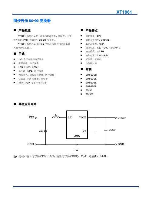
同步升压DC-DC 变换器■ 产品概述XT1861 系列产品是一款低功耗高效率、低纹波、工作频率高的 PFM 控制升压DC-DC 变换器。
XT1861 系列产品仅需要3个外部元器,即可完成低输入的电池电压输入。
■ 用途● 1~3 个干电池的电子设备 ● 数码相机、电子词典 ● LED 手电筒、LED 灯 ● 血压计、MP3、遥控玩具● 无线耳机、无线鼠标键盘、医疗器械 ● 防丢器、汽车防盗器、充电器 ●VCR 、PDA 等手持电子设备■ 产品特点● 最高效率:94% ● 最高工作频率:300KHz ● 低静态电流:15µA● 输出电压:1.8V ~5.0V (步进0.1V ) ● 输出精度:±2.5% ● 输入电压:0.9V ~6.5V ● 低纹波,低噪声 ●小体积封装■ 封装● SOT-23-3B ● SOT-23-3L ● SOT-23-5L● SOT-89-3L ● TO-92 ●TO-92S■ 典型应用电路VINGNDGND VOUT注:建议:输入电容器(CIN):10µF ;输出电容器(COUT):22µF ,电感(L):10uH 。
■ 订购信息XT1861 B ①②③④⑤■ 引脚配置CE VOUT NC LXSOT-23-5L (TOP VIEW)GNDGND VOUTLX SOT-23-3L (TOP VIEW)GND VOUT LX SOT-89-3L (TOP VIEW)TO-92(FRONT VIEW)GND VOUT LXTO-92S (FRONT VIEW)GND VOUT LX12312345123123123■ 引脚分配■ 打印信息SOT-23-3L/B, SOT-23-5L, SOT-89-3L, TO-92, TO-92SSOT-89-3L (TOP VIEW)TO-92(FRONT VIEW)① ② ③ ④......SOT-23-5L (TOP VIEW)SOT-23-3L (TOP VIEW)① ② ③ ④......① ② ③ ④......① ② ③ ④......TO-92S (FRONT VIEW)①②③④......① 表示产品系列② 代表输出电压范围③ 代表输出电压④ 代表生产批号数字0-9,A-Z ,倒写数字0-9,A-Z ,然后重复(G ,I ,J ,O ,Q ,W 除外) 例如:A6TX ,代表XT1861B552*R ,输出电压5.5V 。
GM2001无电感5V输出电荷泵型降压稳压芯片1、产品简介GM2001是一款5V输出电荷泵型降压稳压芯片,输入电压范围宽达6~28V,最大输出电流能力达150mA,内部采用固定900KHz开关频率,同时芯片内部还集成了短路保护、过流保护、过热保护等单元提升可靠性,ESD HBM高达±6000V。
与传统的降压芯片相比,GM2001无需外围的电感和肖特基二极管,应用方案简洁,仅需要3个外围电容。
同时由于无电感器件,芯片的EMI要大幅度低于有电感的开关电源方案,并且在输出电压纹波方面也具有优越的性能。
而与LDO类型的稳压芯片相比,GM2001在效率方面具有极高优势,当输入电压高于10.5V时,转换效率会增加一倍,最高转换效率高达81%,但输出电压噪声又不会增加过多,因此GM2001可以直接取代LDO。
尤其在智能电表和水表及其通信模块等工业领域,GM2001是一款具有优越性价比的稳压电源芯片。
2、应用范围■工业控制■电表、水表、气表■汽车电子3、特色■工作电压:6~28V■输出电压:5V±5%■输出电流:150mA max■ESD HBM±6KV■固定频率:900KHz■低纹波:<8mV■过流保护■过热保护■短路保护■温度范围-40℃to+85℃■应用成本低:无需电感、肖特基二极管、外围器件极少4、封装类型■EMSOP85、功能引脚定义图1、GM2001Top View 序号名称说明1VIN输入引脚2NC3GND接地4CP飞电容正端5CN飞电容负端6NC7NC8VOUT输出引脚注意:EP必须在PCB设计时接露铜散热区6、典型应用电路图2典型应用电路图7、极限参数符号说明大小单位VCC最大输入端电压30VTj最大结温170℃Θja热阻40℃/W Tstg储存温度-60~160℃Pd最大消耗功率(ESOP8) 1.5WESD HBM6000V8、电气特性(各外围参数如图2所示,VDD=12V,TA=+25℃,除非特别注明)参数符号条件最小典型最大单位输入电压VCC628V输出电压VOUT VCC:7~28V 4.75 5.3V电压精度△Vout±5%静态电流Iin空载 1.1mA输出电流Iout100150mA负载调整Vrl负载电流0~100mA 3.7mV/mA 负载电流50~100mA1mV/mA 输入调整Vri VCC:7~28V1mV/V 开关频率Fosc900KHz电源抑制PSRR1Hz~10Mhz50dB输出纹波Riple负载电流=100mA57mV负载电流=15mA1mV短路电流Ishort输出短路到地22mA过流保护Ip200mA热保护点Tp150℃Thys20℃热保护迟滞9、典型特性图3、转换效率VS.输入电压(Iout=100mA)图4、转换效率VS.输出电流(VIN=12V)图5、输入端纹波(Iout=100mA)图6、输出端纹波(Iout=100mA)图7、负载响应CH1:Iout25mA/Div CH2:Vout20mV/Div100us/Div图8、输入响应图9、开关频率VS.温度图10、电源抑制比图11、输出纹波频谱(Iout=100mA)图12、输出纹波频谱(Iout=10mA)10、应用说明概述GM2001是一款电荷泵降压型稳压芯片,可以提供稳定的5V输出,最大输出电流能力达150mA。
用升压型DCDC做sepic升降压电路经验摘要:有很多网友都试验过用升压DCDC做自动升降压sepic电路,都以烧毁器件告终,本文阐述了一种烧毁器件的机理,希望网友门注意。
用TD8208做sepic电路,试图达到如下需求:1.输入是带充电器的锂电池电路,有USB外接电源时,自动用外接5V电源,否则用锂电池电源,故输入电压范围为2.6V-5.2V,其中锂电池供电时电压范围是2.6V-4.2V。
2.输出为3.3V或4.1V。
sepic电路拓扑:实际电路:TD8208(兼容替代型号CE8303/FP6291/MT3608/STI3508/SY7152/SY7208)的典型应用是boost电路,从datasheet中截取如下图,要修改为满足需求的sepic电路需要将下图中红叉位置断开,串入一个电容,再对地接一个电感,如上图中的C1和L2.同时需要修改R2。
R2为150K时,输出电压为3.5V左右。
试验结果:当输入电压从2.6V开始上升,步进0.1V,在低于4V时,输出电压一直维持在3.5V,非常稳定,但当电压上升到4V以上时,输入电流立即剧增,若输入无限流装置芯片立即损坏。
结论是电路末达到设计要求。
原因分析:对比测试TD8208在标准boot模式下LX端子的波形,发现波形尖峰顶部始终没有超过8V,而在sepic模式下,在输入电压末达到4V左右时就几乎达到8V,且顶部平坦,当电压继续升高时,会继续升高,随即产生很大的输入电流,估计是内部保护动作了。
标准boot模式下LX端子的波形查阅datashee发现:TD8208的LX端子电压最大为7V,估计厂家是在内部做了保护,估计是这个保护电压对电路产生了影响。
分析sepic电路结构,发现LX端子电压要比标准boost电路时高。
内部MOS管导通时内部MOS管断开时可以看到,内部MOS管断开时,LX电压是L1上的电压+L2上的电压,而L2的电压是C1在MOS管导通时充的,故LX端电压基本上是2Vo。
w w w .h x s e m i .c o mF e a t u r e s2.2V Start-up Input Voltage Output Voltage as High as 28V 21V at 700mA from 5V Input Up to 88% EfficiencyProviding Flexibility for Using Internal andExternal Power Switches Small SOT23-6L PackageA p p l i c a t i o n sPDA DSC LCD Panel RF-Tags MP3Portable Instrument Wireless EquipmentD e s c r i p t i o nThe C is a compact, high efficiency, and low voltage step-up DC/DC converter with an Adaptive Current Mode PWM control loop, includes an error amplifier, ramp generator, comparator, switch pass element and driver in which providing a stable and high efficient operation over a wide range of load currents. It operates in stable waveforms without external compensation.HX3033 can operate from an input voltage as low as 2.2V. HX3033 can generate 21V up to 700mA from a 5V supply.The HX3033 is available in a low profile SOT-23-6L package.13509685286尚亿微电子李华T y p ic alA p p l i ca t i o n C i r c u i t* V OUT = 1.212V • [1 + (R1/R2)]P i n A s s i g n m e n t a n d F u n c t i o nAnalog Ground.2 SW Switch Pin. Connect inductor between SW and V Keep these PCB trace lengths as short and wide aspossible to reduce EMI and voltage overshoot. drive is derived from the greater of V Logic Controlled Shutdown Input. EN=High: Normal free running operation. EN=Low:Shutdown, quiescent current<1µA. 5 FBFeedback Input to the g Error Amplifier. Connectresistor divider tap to this pin. 6 PGNDPower Ground.A b s o l u t e M a x i m u m R a t i n g s (N o t e 1)Supply Voltage……………………………………………………………………….... −0.3V to 6.5V SW Pin Switch Voltage…………………………………………………………………−0.3V to 6.5V Other I/O Pin Voltages……………………………………………………….. −0.3V to (VDD + 0.3V) SW Pin Switch Current ………………………………………………………………...……………..1A Package Thermal Resistance (SOT-23-6)………………………………………………280 °C/W Operating Junction Temperature…………………………………………………….…………..125°C Storage Temperature Range ……………………………………………………….−65°C ~ +150°CN o t e 1: Absolute Maximum ratings are threshold limit values that must not be exceeded even for an instant under any conditions. Moreover, such values for any two items must not be reached simultaneously. Operation above these absolute maximum ratings may cause degradation or permanent damage to the device. These are stress ratings only and do not necessarily imply functional operation below these limits.E l e c t r i c a l C h a r a c t e r i s t i c s℃V IN=5V, V OUT set to 21V, unless otherwise specified.Operating Conditions: T A=25,Parameter Test Conditions MIN TYP MAX UNITS Start-UP Voltage I OUT = 1mA 2.2 V Operating VDD Range VDD Pin Voltage 2.5 5 V Supply Current (Quiescent) V FB = 1.2V 1300 μA Supply Current (Shutdown) EN = 0V 160 μA Feedback Reference Voltage 1.187 1.212 1.236 V Switching Frequency I OUT = 500mA 780 KHz Maximum Duty 100 % SW ON Resistance 0.3 ΩEN High Threshold V EN Rising 0.8 V EN Low Threshold 0.6 V EN Input Bias Current V EN = 0V, 5V 55 μANote: The EN pin shall be tied to VDD pin and inhibit to act the ON/OFF state whenever the VDD pin voltage may reach to 5.5V or above.T y p i c a l P e r f o r m a n c e C h a r a c t e r i s t i c sOperating Conditions: T A =25℃, unless otherwise specified.0.8Load Current(A)Load Current(A)Load Current(A)0.6Load Current(A)Output Voltage vs Load Current(Vout=10V)V OUT RippleV IN =5V, I LOAD =0.5A, V OUT =21VSW 10V/divM 1usB l o c k D i a g r a mA p p l i c a t i o n I n f o r m a t i o nInductor SelectionFor most applications, the value of the inductor will fall in the range of 1μH to 4.7μH. Its value is chosen based on the desired ripple current. Large value inductors lower ripple current and small value inductors result in higher ripple currents. Higher V IN or V OUT also increases the ripple current as shown in equation .A reasonable starting point for setting ripple current is △I L = 0.72A (40% of 1.8A).The DC current rating of the inductor should be at least equal to the maximum load current plus half the ripple current to prevent core saturation. Thus, a 2.16A rated inductor should be enough for most applications (1.8A + 0.36A). For better efficiency, choose a low DC-resistance inductor.Different core materials and shapes will change the size/current and price/current relationship of an inductor. Toroid or shielded pot cores in ferrite or perm alloy materials are small and don’t radiate much energy, but generally cost more than powdered iron core inductors with similar electrical characteristics. The choice of which style inductor to use often depends more on the price vs. size requirements and any radiated field/EMI requirements than on what VOUT5 requires to operate.Output and Input Capacitor SelectionIn continuous mode, the source current of the top MOSFET is a square wave of duty cycle V OUT/V IN. To prevent large voltage transients, a low ESR input capacitor sized for the maximum RMS current must be used. The maximum RMS capacitor current is given by:This formula has a maximum at V IN = 2V OUT, where I RMS = I OUT/2. This simple worst-case condition is commonly used for design because even significant deviations do not offer much relief. Note that the capacitor manufacturer’s ripple current ratings are often based on 2000 hours of life. This makes it advisable to further derate the capacitor, or choose a capacitor rated at a higher temperature than required. Always consult the manufacturer if there is any question.The selection of C OUT is driven by the required effective series resistance (ESR).Typically, once the ESR requirement for C OUT has been met, the RMS current rating generally far exceeds the I RIPPLE(P-P) requirement. The output ripple ΔV OUT is determined by:Where f = operating frequency, C OUT = output capacitance and ΔI L = ripple current in the inductor. For a fixed output voltage, the output ripple is highest at maximum input voltage since ΔI L increases with input voltage.Aluminum electrolytic and dry tantalum capacitors are both available in surface mount configurations. In the case of tantalum, it is critical that the capacitors are surge tested for use in switching power supplies. An excellent choice is the AVX TPS series of surface mount tantalum. These are specially constructed and tested for low ESR.Efficiency ConsiderationsThe efficiency of a switching regulator is equal to the output power divided by the input power times 100%. It is often useful to analyze individual losses to determine what is limiting the efficiency and which change would produce the most improvement. Efficiency can be expressed as: Efficiency = 100% - (L1+ L2+ L3+ ...) where L1, L2, etc. are the individual losses as a percentage of input power. Although all dissipative elements in the circuit produce losses, two main sources usually account for most of the losses: VIN quiescent current and I2R losses. The VIN quiescent current loss dominates the efficiency loss at very low load currents whereas the I2R loss dominates the efficiency loss at medium to high load currents. In a typical efficiency plot, the efficiency curve at very low load currents can be misleading since the actual power lost is of no consequence.1. The VIN quiescent current is due to two components: the DC bias current as given in the electrical characteristics and the internal main switch and synchronous switch gate charge currents. The gate charge current results from switching the gate capacitance of the internal power MOSFET switches. Each time the gate is switched from high to low to high again, a packet of charge △Q moves from VIN to ground. The resulting△Q/△t is the current out of VIN that is typically larger than the DC bias current. In continuous mode, I GATECHG = f (Q T+Q B) where Q T and Q B are the gate charges of the internal top and bottom switches. Both the DC bias and gate charge losses are proportional to VIN and thus their effects will be more pronounced at higher supply voltages.2. I2R losses are calculated from the resistances of the internal switches, R SW and external inductorR L. In continuous mode the average output current flowing through inductor L is “chopped” between the main switch and the synchronous switch. Thus, the series resistance looking into the SW pin is a function of both top and bottom MOSFET R DS(ON) and the duty cycle (DC) as follows: R SW =R DS(ON)TOP x DC + R DS(ON)BOT x (1-DC) The R DS(ON) for both the top and bottom MOSFETs can be obtained from the Typical Performance Characteristics curves. Thus, to obtain I2R losses, simply addR SW to R L and multiply the result by the square of the average output current. Other losses including CIN and COUT ESR dissipative losses and inductor core losses generally account for less than 2%of the total loss.Board Layout SuggestionsWhen laying out the printed circuit board, the following checklist should be used to ensure proper operation of the HX3033. Check the following in your layout:1. The power traces, consisting of the GND trace, the SW trace and the VIN trace should be keptshort, direct and wide.2. Put the input capacitor as close as possible to the device pins (VIN and GND).3. SW node is with high frequency voltage swing and should be kept small area. Keep analogcomponents away from SW node to prevent stray capacitive noise pick-up.4. Connect all analog grounds to a command node and then connect the command node to the powerground behind the output capacitors.P a c k a g i n g I n f o r m a t i o nSOT-23-6L Package Outline DimensionSymbolDimensions In Millimeters Dimensions In Inches MinMaxMinMaxA 1.050 1.250 0.041 0.049 A1 0.000 0.100 0.000 0.004 A2 1.0501.150 0.041 0.045b 0.300 0.500 0.012 0.020c 0.100 0.200 0.004 0.008 D 2.820 3.020 0.111 0.119 E 1.500 1.700 0.059 0.067 E1 2.6502.950 0.104 0.116e 0.950(BSC)0.037(BSC)e1 1.800 2.000 0.071 0.079 L 0.300 0.600 0.012 0.024 θ 0°8° 0° 8°。
HX1001 T i n y P a c k a g e,H i g h E f f i c i e n c y,S t e p-u pF e a t u r e sInput Voltage Range: 1.1V~5.5V Internal MOSFET with high switch current up to 3A90% EfficiencyUp to 450kHz Switching Frequency SOT-23-6L PackageA p p l i c a t i o n sPDADSCLCD PanelRF-TagsMP3Portable InstrumentsWireless Equipments D e s c r i p t i o nThe HX3141 is a compact, high efficiency, and low voltage step-up DC/DC converter including an error amplifier, ramp generator, comparator, switch pass element and driver in which providing a stable and high efficient operation over a wide range of load currents. It operates in stable waveforms without external compensation.The high switching rate minimized the size of external components. Besides, the low quiescent current together with high efficiency maintains long battery lifetime. The output voltage is set with two external resistors.The HX3141 is available in the industry standard SOT-23-6L power packages.T y p i c a l A p p l i c a t i o n C i r c u i tFigure 1: (1.1V Stat-up input Voltage)A b s o l u t e M a x i m u m R a t i n g s(Note 1)Supply Voltage……………………………………………………………………………….…−0.3V to 6V SW Pin Switch Voltage…………………………………………………………………………−0.3V to 6V Other I/O Pin Voltages…………………………………………………………………………−0.3V to 6V SW Pin Switch Current ………………………………………………………………...………………..4A Operating Junction Temperature…………………………………………………….……………..125°C Storage Temperature Range …………………………………………………………….−65°C ~ +150°C Lead Temperature (Soldering 10 sec.) …………………………………………………………..+ 300℃Note 1. Stresses listed as the above “Absolute Maximum Ratings” may cause permanent damage to the device. These are for stress ratings. Functional operation of the device at these or any other conditions beyond those indicated in the operational sections of the specifications is not implied. Exposure to absolute maximum rating conditions for extended periods may remain possibility to affect device reliability.P i n D e s c r i p t i o nSOT-23-6LElect r i c a l C h a r a c t e r i s t i c s(V IN = 1.5V, VDD set to 3.3V, TA = 25°C, unless otherwise specified)Parameter Test Conditions Min Typ Max Units Start-UP Voltage ILOAD = 1mA 1.1 V Operating VDD Range VDD pin voltage 1.1 5.5 VNo Load Current I (V IN ) V IN = 1.5V, V OUT = 3.3V 70 µA Feedback Reference Voltage Close Loop, VDD = 3.3V 1.182 1.212 1.242 V Switching Frequency VDD = 3.3V 450 kHzSW ON Resistance VDD = 3.3V0.07 Ω Line Regulation V IN = 1.5 ~ 2.5V, IL = 100mA 25 mV/V Load Regulation V IN = 2.5V, IL = 1 ~ 300mA 0.05 mV/mA En Input High 1 V En Input Low 0.6 V Maximum V RM145mVPIN NUMBER SOT-23-6LPIN NAME FUNCTION 1/3 GND Ground2 SW Switch Node for Output4 FB Feedback5 VDD Output6ENON/OFF Control(High Enable)T y p i c a l P e r f o r m a n c e C h a r a c t e r i s t i c sP i n I n f o r m a t i o nGND (Pin 1/3): Signal and Power Ground. Provide a short direct PCB path between GND and the (–) side of the output capacitor(s).SW (Pin 2): Switch Pin. Connect inductor between SW and V IN . Keep these PCB trace lengths as short and wide as possible to reduce EMI and voltage overshoot.FB (Pin 4): Feedback Input to the g m Error Amplifier. Connect resistor divider tap to this pin. The output voltage can be adjusted from 1.8V to 5.5V by: V OUT = 1.212V • [1 + (R1/R2)] VDD (Pin 5): Input positive power pin.EN (Pin 6): En Control Input. Forcing this pin above 1V enables the part. Forcing this pin below 0.6V shuts down the device. Do not leave EN floating.A p p l i c a t i o n I n f o r m a t i o nOutput Voltage SettingReferring to Typical Application Circuits, the output voltage of the switching regulator (V OUT) can be set with Equation (1).Feedback Loop DesignReferring to the Typical Application Circuits. The selection of R1 and R2 based on the trade-off between quiescent current consumption and interference immunity is stated below:Follow Equation (1)Higher R reduces the quiescent current (Path current = 1.212V/R2), however resistors beyond 5MW are not Recommended.Lower R gives better noise immunity, and is less sensitive to interference, layout parasitics, FB node leakage, and improper probing to FB pin.For applications without standby or suspend modes, lower values of R1 and R2 are preferred. For applications concerning the current consumption in standby or suspend modes, the higher values of R1 and R2 are needed. Such high impedance feedback loop is sensitive to any interference, which requires careful PCB layout and avoid any interference, especially to FB pin. To improve the system stability, a proper value capacitor between FB pin and GND pin is suggested. An empirical suggestion is around 22pF.PCB Layout GuidePCB Layout shall follow these guidelines for better system stability:A full GND plane without gap break.VDD to GND noise bypass - Short and wide connection for the 20-100uF capacitor between Pin 5 and Pin 1.VIN to GND noise bypass - Add a 10uF capacitor close to L1 inductor, when V IN is not an idea voltage source.Minimized FB node copper area and keep far away from noise sources.P a c k a g i n g I n f o r m a t i o nSOT-23-6L Package Outline DimensionDimensions In Millimeters Dimensions In Inches SymbolMin Max Min MaxA 1.050 1.250 0.041 0.049A1 0.000 0.100 0.000 0.004A2 1.050 1.150 0.041 0.045b 0.300 0.500 0.012 0.020c 0.100 0.200 0.004 0.008D 2.820 3.020 0.111 0.119E 1.500 1.700 0.059 0.067E1 2.650 2.950 0.104 0.116e 0.950(BSC) 0.037(BSC)e1 1.800 2.000 0.071 0.079L 0.300 0.600 0.012 0.024θ0°8°0°8°。