
LM151X2中文资料
- 格式:pdf
- 大小:563.47 KB
- 文档页数:25


LM2586SIMPLE SWITCHER ®3A Flyback Regulator with ShutdownGeneral DescriptionThe LM2586series of regulators are monolithic integrated circuits specifically designed for flyback,step-up (boost),and forward converter applications.The device is available in 4different output voltage versions:3.3V,5.0V,12V,and ad-justable.Requiring a minimum number of external components,these regulators are cost effective,and simple to use.Included in the datasheet are typical circuits of boost and flyback regu-lators.Also listed are selector guides for diodes and capaci-tors and a family of standard inductors and flyback trans-formers designed to work with these switching regulators.The power switch is a 3.0A NPN device that can stand-off 65V.Protecting the power switch are current and thermal limiting circuits,and an undervoltage lockout circuit.This IC contains an adjustable frequency oscillator that can be pro-grammed up to 200kHz.The oscillator can also be synchro-nized with other devices,so that multiple devices can oper-ate at the same switching frequency.Other features include soft start mode to reduce in-rush current during start up,and current mode control for im-proved rejection of input voltage and output load transients and cycle-by-cycle current limiting.The device also has a shutdown pin,so that it can be turned off externally.An output voltage tolerance of ±4%,within specified input volt-ages and output load conditions,is guaranteed for the power supply system.Featuresn Requires few external componentsn Family of standard inductors and transformers n NPN output switches 3.0A,can stand off 65V n Wide input voltage range:4V to 40Vn Adjustable switching frequency:100kHz to 200kHz n External shutdown capabilityn Draws less than 60µA when shut down n Frequency synchronizationnCurrent-mode operation for improved transient response,line regulation,and current limitn Internal soft-start function reduces in-rush current during start-upn Output transistor protected by current limit,under voltage lockout,and thermal shutdownn System output voltage tolerance of ±4%max over line and load conditions Typical Applicationsn Flyback regulator n Forward convertern Multiple-output regulator nSimple boost regulatorConnection DiagramsBent,Staggered Leads 7-Lead TO-220(T)Top ViewBent,Staggered Leads 7-Lead TO-220(T)Side View0125161701251618Order Number LM2586T3.3,LM2586T-5.0,LM2586T-12or LM2586T-ADJ See NS Package Number TA07BSIMPLE SWITCHER ®and Switchers Made Simple®are registered trademarks of National Semiconductor Corporation.July 2005LM2586SIMPLE SWITCHER 3A Flyback Regulator with Shutdown©2005National Semiconductor Corporation Connection Diagrams(Continued)7-Lead TO-263(S)Top View7-Lead TO-263(S)Side View0125161901251620Order number LM2586S-3.3,LM2586S-5.0,LM2586S-12or LM2586S-ADJTape and Reel Order Number LM2586SX-3.3,LM2586SX-5.0,LM2586SX-12or LM2586SX-ADJSee NS Package Number TS7BOrdering InformationPackage TypeNSC Package Order NumberDrawing 7-Lead TO-220Bent,Staggered Leads TA07B LM2586T-3.3,LM2586T-5.0,LM2586T-12,LM2586T-ADJ 7-Lead TO-263TS7B LM2586S-3.3,LM2586S-5.0,LM2586S-12,LM2586S-ADJ 7-Lead TO-263Tape and ReelTS7BLM2586SX-3.3,LM2586SX-5.0,LM2586SX-12,LM2586SX-ADJL M 2586 2Absolute Maximum Ratings(Note1)If Military/Aerospace specified devices are required, please contact the National Semiconductor Sales Office/ Distributors for availability and specifications.Input Voltage−0.4V≤V IN≤45V Switch Voltage−0.4V≤V SW≤65V Switch Current(Note2)Internally Limited Compensation Pin Voltage−0.4V≤V COMP≤2.4V Feedback Pin Voltage−0.4V≤V FB≤2V OUT ON/OFF Pin Voltage−0.4V≤V SH≤6V Sync Pin Voltage−0.4V≤V SYNC≤2V Power Dissipation(Note3)Internally Limited Storage Temperature Range−65˚C to+150˚CLead Temperature(Soldering,10sec.)260˚C Maximum Junction Temperature(Note3)150˚C Minimum ESD Rating(C=100pF,R=1.5kΩ)2kVOperating RatingsSupply Voltage4V≤V IN≤40V Output Switch Voltage0V≤V SW≤60V Output Switch Current I SW≤3.0A Junction Temp.Range−40˚C≤T J≤+125˚CElectrical CharacteristicsSpecifications with standard type face are for T J=25˚C,and those in bold type face apply over full Operating Temperature Range.Unless otherwise specified,V IN=5V.LM2586-3.3Symbol Parameters Conditions Typical Min Max Units SYSTEM PARAMETERS Test Circuit of Figure1(Note4)V OUT Output Voltage V IN=4V to12V 3.3 3.17/3.14 3.43/3.46VI LOAD=0.3to1.2A∆V OUT/Line Regulation V IN=4V to12V2050/100mV ∆V IN I LOAD=0.3A∆V OUT/Load Regulation V IN=12V2050/100mV ∆I LOAD I LOAD=0.3A to1.2AηEfficiency V IN=5V,I LOAD=0.3A76% UNIQUE DEVICE PARAMETERS(Note5)V REF Output Reference Measured at Feedback Pin 3.3 3.242/3.234 3.358/3.366V Voltage V COMP=1.0V∆V REF Reference Voltage V IN=4V to40V 2.0mV Line RegulationG M Error Amp I COMP=−30µA to+30µA 1.1930.678 2.259mmhoTransconductance V COMP=1.0VA VOL Error Amp V COMP=0.5V to1.6V260151/75V/VVoltage Gain R COMP=1.0MΩ(Note6)LM2586-5.0Symbol Parameters Conditions Typical Min Max Units SYSTEM PARAMETERS Test Circuit of Figure1(Note4)V OUT Output Voltage V IN=4V to12V 5.0 4.80/4.75 5.20/5.25VI LOAD=0.3A to1.1A∆V OUT/Line Regulation V IN=4V to12V2050/100mV ∆V IN I LOAD=0.3A∆V OUT/Load Regulation V IN=12V2050/100mV ∆I LOAD I LOAD=0.3A to1.1AηEfficiency V IN=12V,I LOAD=0.6A80% UNIQUE DEVICE PARAMETERS(Note5)V REF Output ReferenceVoltage Measured at Feedback PinV COMP=1.0V5.0 4.913/4.900 5.088/5.100VLM25863Electrical Characteristics (Continued)LM2586-5.0(Continued)Symbol Parameters ConditionsTypical Min Max Units ∆V REF Reference Voltage V IN =4V to 40V3.3mVLine Regulation G M Error Amp I COMP =−30µA to +30µA 0.7500.447 1.491mmho Transconductance V COMP =1.0V A VOLError Amp V COMP =0.5V to 1.6V 16599/49V/VVoltage GainR COMP =1.0M Ω(Note 6)LM2586-12Symbol Parameters ConditionsTypical Min Max Units SYSTEM PARAMETERS Test Circuit of Figure 2(Note 4)V OUT Output Voltage V IN =4V to 10V 12.011.52/11.4012.48/12.60VI LOAD =0.2A to 0.8A ∆V OUT /Line RegulationV IN =4V to 10V 20100/200mV∆V IN I LOAD =0.2A ∆V OUT /Load RegulationV IN =10V20100/200mV∆I LOAD I LOAD =0.2A to 0.8A ηEfficiency V IN =10V,I LOAD =0.6A 93%UNIQUE DEVICE PARAMETERS (Note 5)V REF Output Reference Measured at Feedback Pin 12.011.79/11.7612.21/12.24VVoltageV COMP =1.0V ∆V REF Reference Voltage V IN =4V to 40V7.8mVLine Regulation G M Error Amp I COMP =−30µA to +30µA 0.3280.1860.621mmhoTransconductance V COMP =1.0V A VOLError Amp V COMP =0.5V to 1.6V 7041/21V/VVoltage GainR COMP =1.0M Ω(Note 6)LM2586-ADJSymbol ParametersConditionsTypical Min Max Units SYSTEM PARAMETERS Test Circuit of Figure 2(Note 4)V OUT Output Voltage V IN =4V to 10V 12.011.52/11.4012.48/12.60VI LOAD =0.2A to 0.8A ∆V OUT /Line RegulationV IN =4V to 10V 20100/200mV∆V IN I LOAD =0.2A ∆V OUT /Load RegulationV IN =10V20100/200mV∆I LOAD I LOAD =0.2A to 0.8A ηEfficiency V IN =10V,I LOAD =0.6A 93%UNIQUE DEVICE PARAMETERS (Note 5)V REF Output Reference Measured at Feedback Pin 1.2301.208/1.2051.252/1.255VVoltageV COMP =1.0V ∆V REF Reference Voltage V IN =4V to 40V1.5mVLine Regulation G M Error Amp I COMP =−30µA to +30µA 3.2001.8006.000mmhoTransconductance V COMP =1.0VA VOLError Amp Voltage GainV COMP =0.5V to 1.6V,R COMP =1.0M Ω(Note 6)670400/200V/VL M 2586 4LM2586 Electrical Characteristics(Continued)LM2586-ADJ(Continued)Symbol Parameters Conditions Typical Min Max UnitsI B Error Amp V COMP=1.0V125425/600nAInput Bias CurrentCOMMON DEVICE PARAMETERS for all versions(Note5)I S Input Supply Current Switch Off(Note8)1115.5/16.5mAI SWITCH=1.8A50100/115mAI S/D Shutdown Input V SH=3V16100/300µASupply CurrentV UV Input Supply R LOAD=100Ω 3.30 3.05 3.75V Undervoltage Lockoutf O Oscillator Frequency Measured at Switch PinR LOAD=100Ω,V COMP=1.0V10085/75115/125kHzFreq.Adj.Pin Open(Pin1)R SET=22kΩ200kHzf SC Short-Circuit Measured at Switch PinFrequency R LOAD=100Ω25kHzV FEEDBACK=1.15VV EAO Error Amplifier Upper Limit 2.8 2.6/2.4V Output Swing(Note7)Lower Limit0.250.40/0.55V(Note8)I EAO Error Amp(Note9)Output Current165110/70260/320µA(Source or Sink)I SS Soft Start Current V FEEDBACK=0.92V11.08.0/7.017.0/19.0µAV COMP=1.0VD MAX Maximum Duty Cycle R LOAD=100Ω9893/90%(Note7)I L Switch Leakage Switch Off15300/600µACurrent V SWITCH=60VV SUS Switch Sustaining Voltage dV/dT=1.5V/ns65VV SAT Switch Saturation Voltage I SWITCH=3.0A0.450.65/0.9VI CL NPN Switch Current Limit 4.0 3.07.0AV STH Synchronization F SYNC=200kHz0.750.625/0.400.875/1.00V Threshold Voltage V COMP=1V,V IN=5VI SYNC Synchronization V IN=5V100200µAPin Current V COMP=1V,V SYNC=V STHV SHTH ON/OFF Pin(Pin1)V COMP=1V 1.6 1.0/0.8 2.2/2.4V Threshold Voltage(Note10)I SH ON/OFF Pin(Pin1)V COMP=1V4015/1065/75µACurrent V SH=V SHTH5Electrical Characteristics (Continued)LM2586-ADJ(Continued)Symbol ParametersConditionsTypical Min Max UnitsCOMMON DEVICE PARAMETERS for all versions (Note 5)θJA Thermal ResistanceT Package,Junction to Ambient (Note 11)65˚C/WθJA T Package,Junction to Ambient (Note 12)45θJC T Package,Junction to Case 2θJA S Package,Junction to Ambient (Note 13)56θJA S Package,Junction to Ambient (Note 14)35θJA S Package,Junction to Ambient (Note 15)26θJCS Package,Junction to Case2Note 1:Absolute Maximum Ratings indicate limits beyond which damage to the device may occur.These ratings apply when the current is limited to less than 1.2mA for pins 1,2,3,and 6.Operating ratings indicate conditions for which the device is intended to be functional,but device parameter specifications may not be guaranteed under these conditions.For guaranteed specifications and test conditions,see the Electrical Characteristics.Note 2:Note that switch current and output current are not identical in a step-up regulator.Output current cannot be internally limited when the LM2586is used as a step-up regulator.To prevent damage to the switch,the output current must be externally limited to 3A.However,output current is internally limited when the LM2586is used as a flyback regulator (see the Application Hints section for more information).Note 3:The junction temperature of the device (T J )is a function of the ambient temperature (T A ),the junction-to-ambient thermal resistance (θJA ),and the power dissipation of the device (P D ).A thermal shutdown will occur if the temperature exceeds the maximum junction temperature of the device:P D x θJA +T A(MAX)≥T J(MAX).For a safe thermal design,check that the maximum power dissipated by the device is less than:P D ≤[T J(MAX)−T A(MAX)]/θJA .When calculating the maximum allowable power dissipation,derate the maximum junction temperature —this ensures a margin of safety in the thermal design.Note 4:External components such as the diode,inductor,input and output capacitors can affect switching regulator performance.When the LM2586is used as shown in Figures 1,2,system performance will be as specified by the system parameters.Note 5:All room temperature limits are 100%production tested,and all limits at temperature extremes are guaranteed via correlation using standard Statistical Quality Control (SQC)methods.Note 6:A 1.0M Ωresistor is connected to the compensation pin (which is the error amplifier output)to ensure accuracy in measuring A VOL .Note 7:To measure this parameter,the feedback voltage is set to a low value,depending on the output version of the device,to force the error amplifier output high and the switch on.Note 8:To measure this parameter,the feedback voltage is set to a high value,depending on the output version of the device,to force the error amplifier output low and the switch off.Note 9:To measure the worst-case error amplifier output current,the LM2586is tested with the feedback voltage set to its low value (Note 7)and at its high value (Note 8).Note 10:When testing the minimum value,do not sink current from this pin —isolate it with a diode.If current is drawn from this pin,the frequency adjust circuit will begin operation (see Figure 41).Note 11:Junction to ambient thermal resistance (no external heat sink)for the 7lead TO-220package mounted vertically,with 1⁄2inch leads in a socket,or on a PC board with minimum copper area.Note 12:Junction to ambient thermal resistance (no external heat sink)for the 7lead TO-220package mounted vertically,with 1⁄2inch leads soldered to a PC board containing approximately 4square inches of (1oz.)copper area surrounding the leads.Note 13:Junction to ambient thermal resistance for the 7lead TO-263mounted horizontally against a PC board area of 0.136square inches (the same size as the TO-263package)of 1oz.(0.0014in.thick)copper.Note 14:Junction to ambient thermal resistance for the 7lead TO-263mounted horizontally against a PC board area of 0.4896square inches (3.6times the area of the TO-263package)of 1oz.(0.0014in.thick)copper.Note 15:Junction to ambient thermal resistance for the 7lead TO-263mounted horizontally against a PC board copper area of 1.0064square inches (7.4times the area of the TO-263package)of 1oz.(0.0014in.thick)copper.Additional copper area will reduce thermal resistance further.See the thermal model in Switchers Made Simple ®software.L M 2586 6Typical Performance CharacteristicsSupply Current vs TemperatureReference Voltage vs Temperature0125160201251603∆Reference Voltage vs Supply Voltage Supply Current vs Switch Current0125160401251605Current Limit vs Temperature Feedback Pin Bias Current vs Temperature0125160601251607LM25867Typical Performance Characteristics(Continued)Switch Saturation Voltage vs TemperatureSwitch Transconductancevs Temperature0125160801251609Oscillator Frequency vs Temperature Error Amp Transconductancevs Temperature0125161001251611Error Amp Voltage Gain vs Temperature Short Circuit Frequencyvs Temperature0125161201251613L M 2586 8Typical Performance Characteristics(Continued)Shutdown Supply Currentvs TemperatureON/OFF Pin Currentvs Voltage0125161401251615Oscillator Frequencyvs Resistance01251616Flyback Regulator01251601LM25869Test Circuits01251621C IN1—100µF,25V Aluminum Electrolytic C IN2—0.1µF CeramicT —22µH,1:1Schott #67141450D —1N5820C OUT —680µF,16V Aluminum Electrolytic C C —0.47µF Ceramic R C —2kFIGURE 1.LM2586-3.3and LM2586-5.001251622C IN1—100µF,25V Aluminum Electrolytic C IN2—0.1µF Ceramic L —15µH,Renco #RL-5472-5D —1N5820C OUT —680µF,16V Aluminum Electrolytic C C —0.47µF Ceramic R C —2kFor 12V Devices:R1=Short (0Ω)and 2=OpenFor ADJ Devices:R1=48.75k,±0.1%and 2=5.62k,±0.1%FIGURE 2.LM2586-12and LM2586-ADJL M 2586 10Flyback Regulator OperationThe LM2586is ideally suited for use in the flyback regulator topology.The flyback regulator can produce a single output voltage,such as the one shown in Figure4,or multiple output voltages.In Figure4,the flyback regulator generates an output voltage that is inside the range of the input voltage. This feature is unique to flyback regulators and cannot be duplicated with buck or boost regulators.The operation of a flyback regulator is as follows(refer to Figure4):when the switch is on,current flows through the primary winding of the transformer,T1,storing energy in the magnetic field of the transformer.Note that the primary and secondary windings are out of phase,so no current flows through the secondary when current flows through the pri-mary.When the switch turns off,the magnetic field col-lapses,reversing the voltage polarity of the primary and secondary windings.Now rectifier D1is forward biased and current flows through it,releasing the energy stored in the transformer.This produces voltage at the output.The output voltage is controlled by modulating the peak switch current.This is done by feeding back a portion of the output voltage to the error amp,which amplifies the differ-ence between the feedback voltage and a1.230V reference. The error amp output voltage is compared to a ramp voltage proportional to the switch current(i.e.,inductor current dur-ing the switch on time).The comparator terminates the switch on time when the two voltages are equal,thereby controlling the peak switch current to maintain a constant output voltage.Block Diagram01251623 For Fixed Versions3.3V,R1=3.4k,R2=2k5.0V,R1=6.15k,R2=2k12V,R1=8.73k,R2=1kFor Adj.VersionR1=Short(0Ω),R2=OpenFIGURE3.Block Diagram LM2586Flyback Regulator Operation(Continued)Typical Performance Characteristics01251624As shown in Figure 4,the LM2586can be used as a flyback regulator by using a minimum number of external components.The switching waveforms of this regulator are shown in Figure 5.Typical Performance Characteristics observed during the operation of this circuit are shown in Figure 6.FIGURE 4.12V Flyback Regulator Design Example01251665A:Switch Voltage,20V/div B:Switch Current,2A/divC:Output Rectifier Current,2A/divD:Output Ripple Voltage,50mV/div AC-CoupledFIGURE 5.Switching WaveformsL M 2586Typical Performance Characteristics(Continued)Typical Flyback Regulator ApplicationsFigure 7through Figure 12show six typical flyback applica-tions,varying from single output to triple output.Each draw-ing contains the part number(s)and manufacturer(s)for every component except the transformer.For the trans-former part numbers and manufacturers’names,see thetable in Figure 13.For applications with different output voltages —requiring the LM2586-ADJ —or different output configurations that do not match the standard configurations,refer to the Switchers Made Simple software.01251666FIGURE 6.V OUT Response to Load Current Step01251627FIGURE 7.Single-Output Flyback RegulatorLM2586Typical Flyback Regulator Applications(Continued)01251628FIGURE 8.Single-Output Flyback Regulator01251629FIGURE 9.Single-Output Flyback RegulatorL M 2586Typical Flyback Regulator Applications(Continued)01251630FIGURE10.Dual-Output Flyback Regulator01251631FIGURE11.Dual-Output Flyback Regulator LM2586Typical Flyback Regulator Applications(Continued)TRANSFORMER SELECTION (T)Figure 13lists the standard transformers available for fly-back regulator applications.Included in the table are the turns ratio(s)for each transformer,as well as the output voltages,input voltage ranges,and the maximum load cur-rents for each circuit.01251632FIGURE 12.Triple-Output Flyback RegulatorApplications Figure 7Figure 8Figure 9Figure 10Figure 11Figure 12Transformers T7T7T7T6T6T5V IN 4V–6V 4V–6V 8V–16V 4V–6V 18V–36V 18V–36V V OUT1 3.3V 5V 12V 12V 12V 5V I OUT1(Max) 1.4A 1A 0.8A 0.15A 0.6A 1.8A N 11111.2 1.20.5V OUT2−12V −12V 12V I OUT2(Max)0.15A 0.6A 0.25A N 2 1.21.21.15V OUT3−12V I OUT3(Max)0.25A N 31.15FIGURE 13.Transformer Selection TableL M 2586Typical Flyback Regulator Applications(Continued)TRANSFORMER FOOTPRINTSFigure15through Figure29show the footprints of eachtransformer,listed in Figure14.TransformerTypeManufacturers’Part NumbersCoilcraft(Note16)Coilcraft(Note16)SurfaceMountPulse(Note17)Surface MountPulse(Note17)Renco(Note18)Schott(Note19)T5Q4338-B Q4437-B PE-68413—RL-553267140890T6Q4339-B Q4438-B PE-68414—RL-553367140900T7S6000-A S6057-A—PE-68482RL-575126606Note16:Coilcraft Inc.,Phone:(800)322-26451102Silver Lake Road,Cary,IL60013Fax:(708)639-1469European Headquarters,21Napier Place Phone:+441236730595Wardpark North,Cumbernauld,Scotland G680LL Fax:+441236730627Note17:Pulse Engineering Inc.,Phone:(619)674-810012220World Trade Drive,San Diego,CA92128Fax:(619)674-8262European Headquarters,Dunmore Road Phone:+3539324107Tuam,Co.Galway,Ireland Fax:+3539324459Note18:Renco Electronics Inc.,Phone:(800)645-582860Jeffryn Blvd.East,Deer Park,NY11729Fax:(516)586-5562Note19:Schott Corp.,Phone:(612)475-11731000Parkers Lane Road,Wayzata,MN55391Fax:(612)475-1786FIGURE14.Transformer Manufacturer GuideT701251633Top ViewFIGURE15.Coilcraft S6000-AT601251634Top ViewFIGURE16.Coilcraft Q4339-BT501251635FIGURE17.Coilcraft Q4437-B(Surface Mount)T501251636Top ViewFIGURE18.Coilcraft Q4338-BLM2586Typical Flyback RegulatorApplications(Continued)T701251637Top ViewFIGURE19.Coilcraft S6057-A(Surface Mount)T601251638Top ViewFIGURE20.Coilcraft Q4438-B(Surface Mount)T701251639Top ViewFIGURE21.Pulse PE-68482T601251640Top ViewFIGURE22.Pulse PE-68414(Surface Mount)T501251642Top ViewFIGURE23.Pulse PE-68413(Surface Mount)T701251643Top ViewFIGURE24.Renco RL-5751T601251645Top ViewFIGURE25.Renco RL-5533T501251646Top ViewFIGURE26.Renco RL-5532LM2586Typical Flyback Regulator Applications(Continued)Step-Up (Boost)Regulator OperationFigure 30shows the LM2586used as a step-up (boost)regulator.This is a switching regulator that produces an output voltage greater than the input supply voltage.A brief explanation of how the LM2586Boost Regulator works is as follows (refer to Figure 30).When the NPN switch turns on,the inductor current ramps up at the rate of V IN /L,storing energy in the inductor.When the switch turns off,the lower end of the inductor flies above V IN ,discharging its current through diode (D)into the output capacitor (C OUT )at a rate of (V OUT −V IN )/L.Thus,energy stored in the inductor during the switch on time is transferred to the output during the switch off time.The output voltage is controlled by adjusting the peak switch current,as described in the flyback regulator section.T701251647Top ViewFIGURE 27.Schott 26606T601251649Top ViewFIGURE 28.Schott 67140900T501251650Top ViewFIGURE 29.Schott 67140890LM2586Step-Up (Boost)Regulator Operation(Continued)By adding a small number of external components (as shown in Figure 30),the LM2586can be used to produce a regulated output voltage that is greater than the applied inputvoltage.The switching waveforms observed during the op-eration of this circuit are shown in Figure 31.Typical perfor-mance of this regulator is shown in Figure 32.01251651FIGURE 30.12V Boost RegulatorL M 2586Typical Performance CharacteristicsTypical Boost Regulator ApplicationsFigures 33,35through Figure 37show four typical boost applications —one fixed and three using the adjustable ver-sion of the LM2586.Each drawing contains the part num-ber(s)and manufacturer(s)for every component.For the fixed 12V output application,the part numbers and manufac-turers’names for the inductor are listed in a table in Figure 34.For applications with different output voltages,refer to the Switchers Made Simple software.01251667A:Switch Voltage,10V/div B:Switch Current,2A/div C:Inductor Current,2A/divD:Output Ripple Voltage,100mV/div,AC-CoupledFIGURE 31.Switching Waveforms01251668FIGURE 32.V OUT Response to Load Current StepLM258621Typical Boost Regulator Applications(Continued)Figure 34contains a table of standard inductors,by part number and corresponding manufacturer,for the fixed out-put regulator of Figure 33.01251654FIGURE 33.+5V to +12V Boost RegulatorCoilcraft (Note 20)Pulse (Note 21)Renco (Note 22)Schott (Note 23)Schott (Note 23)(Surface Mount)DO3316-153PE-53898RL-5471-76714651067146540Note 20:Coilcraft Inc.,Phone:(800)322-26451102Silver Lake Road,Cary,IL 60013Fax:(708)639-1469European Headquarters,21Napier Place Phone:+441236730595Wardpark North,Cumbernauld,Scotland G680LL Fax:+441236730627Note 21:Pulse Engineering Inc.,Phone:(619)674-810012220World Trade Drive,San Diego,CA 92128Fax:(619)674-8262European Headquarters,Dunmore Road Phone:+3539324107Tuam,Co.Galway,Ireland Fax:+3539324459Note 22:Renco Electronics Inc.,Phone:(800)645-582860Jeffryn Blvd.East,Deer Park,NY 11729Fax:(516)586-5562Note 23:Schott Corp.,Phone:(612)475-11731000Parkers Lane Road,Wayzata,MN 55391Fax:(612)475-1786FIGURE 34.Inductor Selection TableL M 2586 22Typical Boost Regulator Applications(Continued)01251655FIGURE 35.+12V to +24V Boost Regulator01251656FIGURE 36.+24V to +36V Boost RegulatorLM258623Typical Boost Regulator Applications(Continued)Note 24:The LM2586will require a heat sink in these applications.The size of the heat sink will depend on the maximum ambient temperature.To calculate the thermal resistance of the IC and the size of the heat sink needed,see the “Heat Sink/Thermal Considerations”section in the Applica-tion Hints.Application HintsLM2586SPECIAL FEATURESSHUTDOWN CONTROLA feature of the LM2586is its ability to be shut down using the ON /OFF pin (pin 1).This feature conserves input power by turning off the device when it is not in use.For proper operation,an isolation diode is required (as shown in Figure 38).The device will shut down when 3V or greater is applied on the ON /OFF pin,sourcing current into pin 1.In shut down mode,the device will draw typically 56µA of supply current (16µA to V IN and 40µA to the ON /OFF pin).To turn the device back on,leave pin 1floating,using an (isolation)diode,as shown in Figure 38(for normal operation,do not source or sink current to or from this pin —see the next section).FREQUENCY ADJUSTMENTThe switching frequency of the LM2586can be adjusted with the use of an external resistor.This feature allows the user to optimize the size of the magnetics and the output capaci-tor(s)by tailoring the operating frequency.A resistor con-nected from pin 1(the Freq.Adj.pin)to ground will set the switching frequency from 100kHz to 200kHz (maximum).As shown in Figure 38,the pin can be used to adjust the frequency while still providing the shut down function.A curve in the Performance Characteristics Section graphs the resistor value to the corresponding switching frequency.The table in Figure 39shows resistor values corresponding to commonly used frequencies.However,changing the LM2586’s operating frequency from its nominal value of 100kHz will change the magnetics selection and compensation component values.01251657FIGURE 37.+24V to +48V Boost Regulator01251658FIGURE 38.Shutdown OperationL M 2586 24Application Hints(Continued)FREQUENCY SYNCHRONIZATIONAnother feature of the LM2586is the ability to synchronizethe switching frequency to an external source,using thesync pin(pin6).This feature allows the user to parallelmultiple devices to deliver more output power.A negative falling pulse applied to the sync pin will synchro-nize the LM2586to an external oscillator(see Figures40,41).Use of this feature enables the LM2586to be synchronizedto an external oscillator,such as a system clock.This opera-tion allows multiple power supplies to operate at the samefrequency,thus eliminating frequency-related noise prob-lems.The scope photo in Figure41shows a LM258612V BoostRegulator synchronized to a200kHz signal.There is a700ns delay between the falling edge of the sync signal and theturning on of the switch.PROGRAMMING OUTPUT VOLTAGE(SELECTING R1AND R2)Referring to the adjustable regulator in Figure42,the outputvoltage is programmed by the resistors R1and R2by thefollowing formula:V OUT=V REF(1+R1/R2)where V REF=1.23VResistors R1and R2divide the output voltage down so thatit can be compared with the1.23V internal reference.WithR2between1k and5k,R1is:R1=R2(V OUT/V REF−1)where V REF=1.23VFor best temperature coefficient and stability with time,use1%metal film resistors.SHORT CIRCUIT CONDITIONDue to the inherent nature of boost regulators,when theoutput is shorted(see Figure42),current flows directly fromthe input,through the inductor and the diode,to the output,bypassing the switch.The current limit of the switch does notlimit the output current for the entire circuit.To protect theload and prevent damage to the switch,the current must beexternally limited,either by the input supply or at the output R SET(kΩ)Frequency(kHz)Open100200125471503317522200FIGURE39.Frequency Setting Resistor Guide01251659FIGURE40.Frequency Synchronization01251669FIGURE41.Waveforms of a Synchronized12V Boost Regulator01251661FIGURE42.Boost RegulatorLM258625。
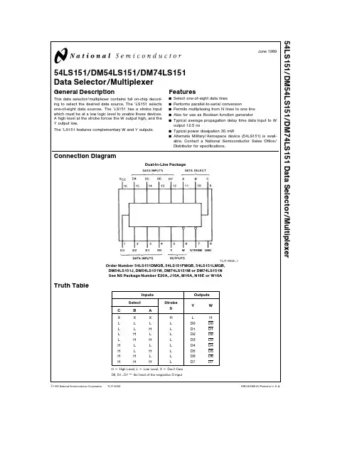
TL F 639254LS151 DM54LS151 DM74LS151 Data Selector MultiplexerJune1989 54LS151 DM54LS151 DM74LS151Data Selector MultiplexerGeneral DescriptionThis data selector multiplexer contains full on-chip decod-ing to select the desired data source The’LS151selectsone-of-eight data sources The’LS151has a strobe inputwhich must be at a low logic level to enable these devicesA high level at the strobe forces the W output high and theY output lowThe’LS151features complementary W and Y outputsFeaturesY Select one-of-eight data linesY Performs parallel-to-serial conversionY Permits multiplexing from N lines to one lineY Also for use as Boolean function generatorY Typical average propagation delay time data input to Woutput12 5nsY Typical power dissipation30mWY Alternate Military Aerospace device(54LS151)is avail-able Contact a National Semiconductor Sales OfficeDistributor for specificationsConnection DiagramDual-In-Line PackageTL F 6392–1Order Number54LS151DMQB 54LS151FMQB 54LS151LMQBDM54LS151J DM54LS151W DM74LS151M or DM74LS151NSee NS Package Number E20A J16A M16A N16E or W16ATruth TableInputs OutputsSelect StrobeY WC B A SX X X H L HL L L L D0D0L L H L D1D1L H L L D2D2L H H L D3D3H L L L D4D4H L H L D5D5H H L L D6D6H H H L D7D7H e High Level L e Low Level X e Don’t CareD0 D1 D7e the level of the respective D inputC1995National Semiconductor Corporation RRD-B30M105 Printed in U S AAbsolute Maximum Ratings(Note)If Military Aerospace specified devices are required please contact the National Semiconductor Sales Office Distributors for availability and specifications Supply Voltage7V Input Voltage7V Operating Free Air Temperature RangeDM54LS and54LS b55 C to a125 C DM74LS0 C to a70 C Storage Temperature Range b65 C to a150 C Note The‘‘Absolute Maximum Ratings’’are those values beyond which the safety of the device cannot be guaran-teed The device should not be operated at these limits The parametric values defined in the‘‘Electrical Characteristics’’table are not guaranteed at the absolute maximum ratings The‘‘Recommended Operating Conditions’’table will define the conditions for actual device operationRecommended Operating ConditionsSymbol ParameterDM54LS151DM74LS151Units Min Nom Max Min Nom MaxV CC Supply Voltage4 555 54 7555 25V V IH High Level Input Voltage22V V IL Low Level Input Voltage0 70 8V I OH High Level Output Current b0 4b0 4mA I OL Low Level Output Current48mA T A Free Air Operating Temperature b55125070 CElectrical Characteristics over recommended operating free air temperature range(unless otherwise noted)Symbol Parameter Conditions MinTypMax Units (Note1)V I Input Clamp Voltage V CC e Min I I e b18mA b1 5V V OH High Level Output V CC e Min I OH e Max DM542 53 4V Voltage V IL e Max V IH e Min DM742 73 4V OL Low Level Output V CC e Min I OL e Max DM540 250 4 Voltage V IL e Max V IH e Min DM740 350 5VI OL e4mA V CC e Min DM740 250 4I I Input Current Max V CC e Max V I e7V0 1mAInput VoltageI IH High Level Input Current V CC e Max V I e2 7V20m A I IL Low Level Input Current V CC e Max V I e0 4V b0 4mAI OS Short Circuit V CC e Max DM54b20b100mA Output Current(Note2)DM74b20b100I CC Supply Current V CC e Max(Note3)610mA Note1 All typicals are at V CC e5V T A e25 CNote2 Not more than one output should be shorted at a time and the duration should not exceed one secondNote3 I CC is measured with all outputs open strobe and data select inputs at4 5V and all other inputs open2Switching Characteristics at V CC e 5V and T A e 25 C (See Section 1for Test Waveforms and Output Load)From (Input)R L e 2k XSymbol ParameterTo (output)C L e 15pF C L e 50pF UnitsMinMax MinMax t PLH Propagation Delay Time Select 4346ns Low to High Level Output (4Levels)to Y t PHL Propagation Delay Time Select 3036ns High to Low Level Output (4Levels)to Y t PLH Propagation Delay Time Select2325ns Low to High Level Output (3Levels)to W t PHL Propagation Delay Time Select3240ns High to Low Level Output (3Levels)to Wt PLH Propagation Delay Time Strobe 4244ns Low to High Level Output to Y t PHL Propagation Delay Time Strobe 3240ns High to Low Level Output to Y t PLH Propagation Delay Time Strobe 2427ns Low to High Level Output to W t PHL Propagation Delay Time Strobe 3036ns High to Low Level Output to W t PLH Propagation Delay Time D0thru D73235ns Low to High Level Output to Y t PHL Propagation Delay Time D0thru D72633ns High to Low Level Output to Y t PLH Propagation Delay Time D0thru D72125ns Low to High Level Output to W t PHLPropagation Delay Time D0thru D72027ns High to Low Level Outputto WLogic DiagramLS151TL F 6392–2See Address Buffers to the RightAddress Buffers for 54LS151 74LS151TL F 6392–33Physical Dimensions inches(millimeters)Ceramic Leadless Chip Carrier Package(E)Order Number54LS151LMQBNS Package Number E20ACeramic Dual-In-Line Package(J)Order Number54LS151DMQB or DM54LS151JNS Package Number J16A4Physical Dimensions inches(millimeters)(Continued)16-Lead Small Outline Molded Package(M)Order Number DM74LS151MNS Package Number M16A16-Lead Molded Dual-In-Line Package(N)Order Number DM74LS151NNS Package Number N16E554L S 151 D M 54L S 151 D M 74L S 151D a t a S e l e c t o r M u l t i p l e x e rPhysical Dimensions inches (millimeters)(Continued)16-Lead Ceramic Flat Package (W)Order Number 54LS151FMQB or DM54LS151WNS Package Number W16ALIFE SUPPORT POLICYNATIONAL’S PRODUCTS ARE NOT AUTHORIZED FOR USE AS CRITICAL COMPONENTS IN LIFE SUPPORT DEVICES OR SYSTEMS WITHOUT THE EXPRESS WRITTEN APPROVAL OF THE PRESIDENT OF NATIONAL SEMICONDUCTOR CORPORATION As used herein 1 Life support devices or systems are devices or 2 A critical component is any component of a life systems which (a)are intended for surgical implant support device or system whose failure to perform can into the body or (b)support or sustain life and whose be reasonably expected to cause the failure of the life failure to perform when properly used in accordance support device or system or to affect its safety or with instructions for use provided in the labeling can effectivenessbe reasonably expected to result in a significant injury to the userNational Semiconductor National Semiconductor National Semiconductor National Semiconductor CorporationEuropeHong Kong LtdJapan Ltd1111West Bardin RoadFax (a 49)0-180-530858613th Floor Straight Block Tel 81-043-299-2309。