
LM79L15ACZ中文资料
- 格式:pdf
- 大小:247.35 KB
- 文档页数:6

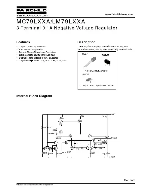
©2002 Fairchild Semiconductor CorporationRev. 1.0.2Features•Output Current up to 100mA •No External Components•Internal Thermal Over Load Protection•Internal Short Circuit Current Limiting •Output V oltage Offered in ±5% Tolerance•Output V oltage of -5V , -8V , -12V , -15V , -18V , -24VDescriptionThese regulators employ internal current limiting and thermal shutdown, making them essentially indestructible.TO-9218-SOPSOT-8911.GND2.Input3.Output 1. Output 2.3.6.7. Input 5. GND4.8. NC1Internal Block DiagramQ1Q2Q3Q4Q5Q6Q7Q8Q9Q10Q11Q12Q13Q14Q15Q16Q17R1R2R3R4R5R6R7R15R16R17R18R26R22R24R25R29R R28R23+R21R27D3D2D1C1GNDOutputInputMC79LXXA/LM79LXXA3-Terminal 0.1A Negative Voltage Regulato rMC79LXXA/LM79LXXA2Absolute Maximum RatingsElectrical Characteristics(MC79L05A/LM79L05A)(V I = -10V, I O = 40mA, C I = 0.33µF, C O = 0.1µF, 0°C ≤T J ≤ +125°C, unless otherwise specified)Note:1. Load and line regulation are specified at constant junction temperature. Change in V O due to heating effects must be takeninto account separately. Pulse testing with low duty is used.ParameterSymbol Value Unit Input Voltage (for V o = -5V to -8V)(for V O = -12V to -18V)(for V O = -24V)V I -30-35-40V Operating Temperature Range T OPR 0 ~ +125°C Storage Temperature RangeT STG-65 ~ +150°CParameter Symbol ConditionsMin.Typ.Max.Unit Output Voltage V O T J = +25°C-4.8-5.0-5.2V Line Regulation (Note1)∆V O T J =+25°C -7.0V ≥ V I ≥ -20V-15150mV -8V ≥ V I ≥ -20V --100mV Load Regulation (Note1)∆V O T J =+25°C1.0mA ≤ I O ≤ 100mA -2060mV 1.0mA ≤ I O ≤ 40mA -1030mV Output Voltage V O -7.0V ≥ V I ≥ -20V, 1.0mA ≤ I O ≤ 40mA -4.75--5.25V V I = -10V, 1.0mA ≤ I O ≤ 70mA -4.75--5.25V Quiescent Current I QT J =+25°C - 2.0 5.5mA T J = +125°C -- 6.0Quiescent Current ChangeWith Line ∆I Q -8V ≥ V I ≥ -20V -- 1.5mA With Load∆I Q 1.0mA ≤ I O ≤ 40mA--0.1mA Output Noise Voltage V N T A = +25°C,10Hz ≤ f ≤ 100kHz -30-µV Ripple Rejection RR f = 120Hz, -8V ≥ V I ≥ -18V T J = +25°C 4160-dB Dropout VoltageV DT J = +25°C- 1.7-VMC79LXXA/LM79LXXA3Electrical Characteristics (MC79L08A) (Continued)(V I = -14V, I O = 40mA, C I = 0.33µF, C O = 0.1µF, 0°C ≤T J ≤ +125°C, unless otherwise specified)Note:1. Load and line regulation are specified at constant junction temperature. Change in V O due to heating effects must be takeninto account separately. Pulse testing with low duty is used.Parameter Symbol ConditionsMin.Typ.Max.Unit Output Voltage V O T J = +25°C-7.7-8.0-8.3V Line Regulation(Note1)∆V O T J = +25°C -10.3V ≥ V I ≥ -23V--175mV -12V ≥ V I ≥ -23V --125mV Load Regulation (Note1)∆V O T J = +25°C1.0mA ≤ I o ≤ 100mA --80mV 1.0mA ≤ I o ≤ 40mA --40mV Output Voltage V O -10.3V ≥ V I ≥ -23V, 1.0mA ≤ I o ≤ 40mA -7.6--8.4V V I = -14V, 1.0mA ≤ I o ≤ 70mA -7.6--8.4Quiescent Current I qT j = +25°C -- 6.0mA T j = +125°C -- 5.5Quiescent Current ChangeWith Line ∆I Q -11.7V ≥ V I ≥ -23V -- 1.5mA With Load1.0mA ≤ I o ≤ 40mA--0.1mA Output Noise Voltage V N T j = +25°C,10Hz ≤ f ≤ 100kHz -50-µV Ripple Rejection RR f = 120Hz, -11V ≥ V I ≥ -21V T j = +25°C 3955-dB Dropout VoltageV DT j = +25°C- 1.7-VMC79LXXA/LM79LXXA4Electrical Characteristics(MC79L12A) (Continued)(V I = -19V, I O = 40mA, C I = 0.33µF, C O = 0.1µF, 0°C ≤T J ≤ +125°C, unless otherwise specified)Note:1. Load and line regulation are specified at constant junction temperature. Change in V O due to heating effects must be takeninto account separately. Pulse testing with low duty is used.Parameter Symbol ConditionsMin.Typ.Max.Unit Output Voltage V O T J = +25°C-11.5-12.0-12.5V Line Regulation (Note1)∆V O T J = +25°C -14.5V ≥ V I ≥ -27V--250mV -16V ≥ V I ≥ -27V --200mV Load Regulation (Note1)∆V O T J = +25°C1.0mA ≤ I O ≤ 100mA --100mV 1.0mA ≤ I O ≤ 40mA --50mV Output Voltage V O -14.5V > V I > -27V, 1.0mA ≤ I O ≤ 40mA -11.4--12.6V V I = -19V, 1.0mA ≤ I O ≤ 70mA -11.4--12.6V Quiescent Current I QT J = +25°C -- 6.0mA T J = +125°C -- 6.5Quiescent Current ChangeWith Line ∆I Q -16V ≥ V I ≥ -27V -- 1.5mA With Load∆I Q 1.0mA ≤ I O ≤ 40mA--0.1mA Output Noise Voltage V N T A = +25°C,10Hz ≤ f ≤ 100kHz -80-µV Ripple Rejection RR f = 120Hz, -15V ≥ V I ≥ -25V T J = +25°C 3742-dB Dropout VoltageV DT J = +25°C- 1.7-VMC79LXXA/LM79LXXA5Electrical Characteristics(MC79L15A) (Continued)(V I = -23V, I O = 40mA, C I = 0.33µF, C O = 0.1µF, 0°C ≤T J ≤ +125°C, unless otherwise specified)Note:1. Load and line regulation are specified at constant junction temperature. Change in V O due to heating effects must be takeninto account separately. Pulse testing with low duty is used.Parameter Symbol ConditionsMin.Typ.Max.Unit Output Voltage V O T J = +25°C-14.4-15.0-15.6V Line Regulation (Note1)∆V O T J = +25°C -17.5V ≥ V I ≥ -30V--300mV -20V ≥ V I ≥ -30V --250mV Load Regulation (Note1)∆V O T J = +25°C1.0mA ≤ I O ≤ 100mA --150mV 1.0mA ≤ I O ≤ 40mA --75mV Output Voltage V O -17.5V ≥ V I ≥ -30V, 1.0mA ≤ I O ≤ 40mA -14.25--15.75V V I = -23V, 1.0mA ≤ I O ≤ 70mA -14.25--15.75V Quiescent Current I QT J = +25°C -- 6.0mA T J = +125°C -- 6.5Quiescent Current ChangeWith Line ∆I Q -20V ≥ V I ≥ -30V -- 1.5mA With Load∆I Q 1.0mA ≤ I O ≤ 40mA--0.1mA Output Noise Voltage V N T A = +25°C,10Hz ≤ f ≤ 100kHz -90-µV Ripple Rejection RR f = 120Hz, -18.5V ≥ V I ≥ -28.5V T J = +25°C 3439-dB Dropout VoltageV DT J = +25°C- 1.7-VMC79LXXA/LM79LXXA6Electrical Characteristics(MC79L18A) (Continued)(V I = -27V, I O = 40mA, C I = 0.33µF, C O = 0.1µF, 0°C ≤T J ≤ +125°C, unless otherwise specified)Note:1. Load and line regulation are specified at constant junction temperature. Change in V O due to heating effects must be takeninto account separately. Pulse testing with low duty is used.Parameter Symbol ConditionsMin.Typ.Max.Unit Output Voltage V O T J = +25°C-17.3-18.0-18.7V Line Regulation (Note1)∆V O T J = +25°C -20.7V ≥ V I ≥ -33V--325mV -21V ≥ V I ≥ -33V --275mV Load Regulation (Note1)∆V O T J = +25°C1.0mA ≤ I O ≤ 100mA --170mV 1.0mA ≤ I O ≤ 40mA --85mV Output Voltage V O -20.7V > V I > -33V, 1.0mA ≤ I O ≤ 40mA -17.1--18.9V V I = -27V, 1.0mA ≤ I O ≤ 70mA -17.1--18.9V Quiescent Current I QT J = +25°C -- 6.5mA T J = +125°C -- 6.0Quiescent Current ChangeWith Line ∆I Q -21V ≥ V I ≥ -33V -- 1.5mA With Load∆I Q 1.0mA ≤ I O ≤ 40mA--0.1mA Output Noise Voltage V N T A =+25°C,10Hz ≤ f ≤ 100kHz -150-µV Ripple Rejection RR f = 120Hz, -23V ≥ V I ≥ -33V T J = +25°C 3348-dB Dropout VoltageV DT J = +25°C- 1.7-VMC79LXXA/LM79LXXA7Electrical Characteristics(MC79L24A) (Continued)(V I = -33V, I O = 40mA, C I = 0.33µF, C O = 0.1µF, 0°C ≤T J ≤ +125°C, unless otherwise specified)Note:1. Load and line regulation are specified at constant junction temperature. Change in V O due to heating effects must be takeninto account separately. Pulse testing with low duty is used.Parameter Symbol ConditionsMin.Typ.Max.Unit Output Voltage V O T J = +25°C-23-24-25V Line Regulation (Note1)∆V O T J = +25°C -27V ≥ V I ≥ -38V--350mV -28V ≥ V I ≥ -38V --300mV Load Regulation (Note1)∆V O T J = +25°C1.0mA ≤ I O ≤ 100mA --200mV 1.0mA ≤ I O ≤ 40mA --100mV Output Voltage V O -27V ≥ V I ≥ -38V, 1.0mA ≤ I O ≤ 40mA -22.8--25.2V V I = -33V, 1.0mA ≤ I O ≤ 70mA -22.8--25.2V Quiescent Current I QT J = +25°C -- 6.5mA T J = +125°C -- 6.0Quiescent Current ChangeWith Line ∆I Q -28V ≥ V I ≥ -38V -- 1.5mA With Load∆I Q 1.0mA ≤ I O ≤ 40mA--0.1mA Output Noise Voltage V N T A = +25°C,10Hz ≤ f ≤ 100kHz -200-µV Ripple Rejection RR f = 120Hz, -29V ≥ V I ≥ -35V T J = +25°C 3147-dB Dropout VoltageV DT J = +25°C- 1.7-VMC79LXXA/LM79LXXA8Typical ApplicationDesign ConsiderationsThe MC79LXXA/LM79LXXA Series of fixed voltage regulators are designed with Thermal Overload Protection that shuts down the circuit when subjected to an excessive power overload condition. Internal Short Circuit Protection that limits the maximum current the circuit will pass. In many low current applications, compensation capacitors are not required. However,it is recommended that the regulator input be bypassed with a capacitor if the regulator is connected to the power supply filter with long wire lengths, or if the output load capacitance is large. An input bypass capacitor should be selected to provide good high frequency characteristics to insure stable operation under all load conditions. A 0.33µF or larger tantalum, mylar, or other capacitor having low internal impedance at high frequencies should be chosen. The bypass capacitor should be mounted with the shortest possible leads directly across the regulator's input terminals. Normally good construction techniques should be used to minimize ground loops and lead resistance drops since the regulator has no external sense lead. Bypassing the output is also recommended.A common ground is required between the Input and the output voltages. The input voltage must remain typically 2.0V above the output voltage even during the low point on the input ripple voltage. * C 1 is required if regulator is located an appreciable distance from power supply filter.* C O improves stability and transient response.Figure 1.Positive And Negative RegulatorFigure 2.Typical ApplicationLM78LXXA MC78LXXALM79LXXA MC79LXXAIMC79LXXA LM79LXXAMC79LXXA/LM79LXXA Mechanical DimensionsPackageDimensions in millimetersTO-929MC79LXXA/LM79LXXAMechanical Dimensions (Continued)PackageDimensions in millimeters8-SOP10MC79LXXA/LM79LXXA Mechanical Dimensions (Continued)PackageDimensions in millimetersSOT-8911MC79LXXA/LM79LXXA12/11/02 0.0m 001Stock#DSxxxxxxxx2002 Fairchild Semiconductor CorporationLIFE SUPPORT POLICYFAIRCHILD’S PRODUCTS ARE NOT AUTHORIZED FOR USE AS CRITICAL COMPONENTS IN LIFE SUPPORT DEVICES OR SYSTEMS WITHOUT THE EXPRESS WRITTEN APPROVAL OF THE PRESIDENT OF FAIRCHILD SEMICONDUCTOR CORPORATION. As used herein:1.Life support devices or systems are devices or systemswhich, (a) are intended for surgical implant into the body, or (b) support or sustain life, and (c) whose failure to perform when properly used in accordance with instructions for use provided in the labeling, can bereasonably expected to result in a significant injury of the user.2. A critical component in any component of a life supportdevice or system whose failure to perform can bereasonably expected to cause the failure of the life support device or system, or to affect its safety or effectiveness.DISCLAIMERFAIRCHILD SEMICONDUCTOR RESERVES THE RIGHT TO MAKE CHANGES WITHOUT FURTHER NOTICE TO ANY PRODUCTS HEREIN TO IMPROVE RELIABILITY, FUNCTION OR DESIGN. FAIRCHILD DOES NOT ASSUME ANYLIABILITY ARISING OUT OF THE APPLICATION OR USE OF ANY PRODUCT OR CIRCUIT DESCRIBED HEREIN; NEITHER DOES IT CONVEY ANY LICENSE UNDER ITS PATENT RIGHTS, NOR THE RIGHTS OF OTHERS.Ordering InformationProduct Number Package Operating TemperatureLM79L05ACZ TO-92 0 ~ +125°C Product Number PackageOperating TemperatureMC79L05ACP TO-920 ~ +125°CMC79L08ACP MC79L12ACP MC79L15ACP MC79L18ACP MC79L24ACP MC79L05ACD 8-SOP MC79L15ACD MC79L05ACHSOT-89。

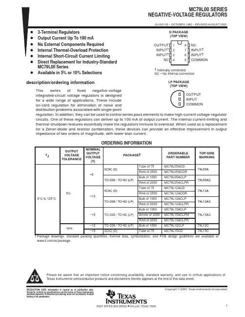
PACKAGING INFORMATIONOrderable Device Status(1)PackageType PackageDrawingPins PackageQtyEco Plan(2)Lead/Ball Finish MSL Peak Temp(3)MC79L05ACD ACTIVE SOIC D875Green(RoHS&no Sb/Br)CU NIPDAU Level-1-260C-UNLIMMC79L05ACDE4ACTIVE SOIC D875Green(RoHS&no Sb/Br)CU NIPDAU Level-1-260C-UNLIMMC79L05ACDG4ACTIVE SOIC D875Green(RoHS&no Sb/Br)CU NIPDAU Level-1-260C-UNLIMMC79L05ACDR ACTIVE SOIC D82500Green(RoHS&no Sb/Br)CU NIPDAU Level-1-260C-UNLIMMC79L05ACDRE4ACTIVE SOIC D82500Green(RoHS&no Sb/Br)CU NIPDAU Level-1-260C-UNLIMMC79L05ACDRG4ACTIVE SOIC D82500Green(RoHS&no Sb/Br)CU NIPDAU Level-1-260C-UNLIM MC79L05ACLP ACTIVE TO-92LP31000TBD CU SNPB Level-NC-NC-NC MC79L05ACLPR ACTIVE TO-92LP32000TBD CU SNPB Level-NC-NC-NC MC79L05AILP OBSOLETE TO-92LP3TBD Call TI Call TIMC79L05CD OBSOLETE SOIC D8TBD Call TI Call TIMC79L05CDR OBSOLETE SOIC D8TBD Call TI Call TIMC79L05CLP OBSOLETE TO-92LP3TBD Call TI Call TIMC79L12ACD ACTIVE SOIC D875Green(RoHS&no Sb/Br)CU NIPDAU Level-1-260C-UNLIMMC79L12ACDE4ACTIVE SOIC D875Green(RoHS&no Sb/Br)CU NIPDAU Level-1-260C-UNLIMMC79L12ACDR ACTIVE SOIC D82500Green(RoHS&no Sb/Br)CU NIPDAU Level-1-260C-UNLIMMC79L12ACDRE4ACTIVE SOIC D82500Green(RoHS&no Sb/Br)CU NIPDAU Level-1-260C-UNLIM MC79L12ACLP ACTIVE TO-92LP31000TBD CU SNPB Level-NC-NC-NC MC79L12ACLPR ACTIVE TO-92LP32000TBD CU SNPB Level-NC-NC-NCMC79L12CD OBSOLETE SOIC D8TBD Call TI Call TIMC79L12CLP ACTIVE TO-92LP31000TBD CU SNPB Level-NC-NC-NC MC79L15ACD OBSOLETE SOIC D8TBD Call TI Call TIMC79L15ACLP ACTIVE TO-92LP31000TBD CU SNPB Level-NC-NC-NC MC79L15ACLPM ACTIVE TO-92LP32000TBD CU SNPB Level-NC-NC-NC MC79L15ACLPR ACTIVE TO-92LP32000TBD CU SNPB Level-NC-NC-NCMC79L15CD ACTIVE SOIC D875Green(RoHS&no Sb/Br)CU NIPDAU Level-1-260C-UNLIMMC79L15CDE4ACTIVE SOIC D875Green(RoHS&no Sb/Br)CU NIPDAU Level-1-260C-UNLIM MC79L15CLP OBSOLETE TO-92LP3TBD Call TI Call TI(1)The marketing status values are defined as follows:ACTIVE:Product device recommended for new designs.LIFEBUY:TI has announced that the device will be discontinued,and a lifetime-buy period is in effect.NRND:Not recommended for new designs.Device is in production to support existing customers,but TI does not recommend using this part in a new design.PREVIEW:Device has been announced but is not in production.Samples may or may not be available.OBSOLETE:TI has discontinued the production of the device.(2)Eco Plan-The planned eco-friendly classification:Pb-Free(RoHS)or Green(RoHS&no Sb/Br)-please check /productcontent for the latest availability information and additional product content details.TBD:The Pb-Free/Green conversion plan has not been defined.Pb-Free(RoHS):TI's terms"Lead-Free"or"Pb-Free"mean semiconductor products that are compatible with the current RoHS requirements for all6substances,including the requirement that lead not exceed0.1%by weight in homogeneous materials.Where designed to be soldered at high temperatures,TI Pb-Free products are suitable for use in specified lead-free processes.Green(RoHS&no Sb/Br):TI defines"Green"to mean Pb-Free(RoHS compatible),and free of Bromine(Br)and Antimony(Sb)based flame retardants(Br or Sb do not exceed0.1%by weight in homogeneous material)(3)MSL,Peak Temp.--The Moisture Sensitivity Level rating according to the JEDEC industry standard classifications,and peak solder temperature.Important Information and Disclaimer:The information provided on this page represents TI's knowledge and belief as of the date that it is provided.TI bases its knowledge and belief on information provided by third parties,and makes no representation or warranty as to the accuracy of such information.Efforts are underway to better integrate information from third parties.TI has taken and continues to take reasonable steps to provide representative and accurate information but may not have conducted destructive testing or chemical analysis on incoming materials and chemicals.TI and TI suppliers consider certain information to be proprietary,and thus CAS numbers and other limited information may not be available for release.In no event shall TI's liability arising out of such information exceed the total purchase price of the TI part(s)at issue in this document sold by TI to Customer on an annual basis.元器件交易网IMPORTANT NOTICETexas Instruments Incorporated and its subsidiaries (TI) reserve the right to make corrections, modifications,enhancements, improvements, and other changes to its products and services at any time and to discontinueany product or service without notice. Customers should obtain the latest relevant information before placingorders and should verify that such information is current and complete. All products are sold subject to TI’s termsand conditions of sale supplied at the time of order acknowledgment.TI warrants performance of its hardware products to the specifications applicable at the time of sale inaccordance with TI’s standard warranty. T esting and other quality control techniques are used to the extent TIdeems necessary to support this warranty. Except where mandated by government requirements, testing of allparameters of each product is not necessarily performed.TI assumes no liability for applications assistance or customer product design. Customers are responsible fortheir products and applications using TI components. T o minimize the risks associated with customer productsand applications, customers should provide adequate design and operating safeguards.TI does not warrant or represent that any license, either express or implied, is granted under any TI patent right,copyright, mask work right, or other TI intellectual property right relating to any combination, machine, or processin which TI products or services are used. Information published by TI regarding third-party products or servicesdoes not constitute a license from TI to use such products or services or a warranty or endorsement thereof.Use of such information may require a license from a third party under the patents or other intellectual propertyof the third party, or a license from TI under the patents or other intellectual property of TI.Reproduction of information in TI data books or data sheets is permissible only if reproduction is withoutalteration and is accompanied by all associated warranties, conditions, limitations, and notices. Reproductionof this information with alteration is an unfair and deceptive business practice. TI is not responsible or liable forsuch altered documentation.Resale of TI products or services with statements different from or beyond the parameters stated by TI for thatproduct or service voids all express and any implied warranties for the associated TI product or service andis an unfair and deceptive business practice. TI is not responsible or liable for any such statements.Following are URLs where you can obtain information on other Texas Instruments products and applicationsolutions:Products ApplicationsAmplifiers Audio /audioData Converters Automotive /automotiveDSP Broadband /broadbandInterface Digital Control /digitalcontrolLogic Military /militaryPower Mgmt Optical Networking /opticalnetworkMicrocontrollers Security /securityTelephony /telephonyVideo & Imaging /videoWireless /wirelessMailing Address:Texas InstrumentsPost Office Box 655303 Dallas, Texas 75265Copyright 2005, Texas Instruments Incorporated。

1/34November 2004s OUTPUT CURRENT TO 1.5AsOUTPUT VOLTAGES OF 5; 5.2; 6; 8; 8.5; 9; 10; 12; 15; 18; 24Vs THERMAL OVERLOAD PROTECTION s SHORT CIRCUIT PROTECTIONsOUTPUT TRANSITION SOA PROTECTIONDESCRIPTIONThe L7800 series of three-terminal positive regulators is available in TO-220, TO-220FP,TO-220FM, TO-3 and D 2PAK packages and several fixed output voltages, making it useful in a wide range of applications. These regulators can provide local on-card regulation, eliminating the distribution problems associated with single point regulation. Each type employs internal current limiting, thermal shut-down and safe area protection, making it essentially indestructible. If adequate heat sinking is provided, they can deliver over 1A output current. Although designed primarily as fixed voltage regulators, these devices can be used with external components to obtain adjustable voltage and currents.L7800SERIESPOSITIVE VOLTAGE REGULATORSL7800 SERIESTable 1: Absolute Maximum RatingsAbsolute Maximum Ratings are those values beyond which damage to the device may occur. Functional operation under these condition is not implied.Table 2: Thermal DataFigure 2: Schematic DiagramSymbol ParameterValue Unit V I DC Input Voltage for V O = 5 to 18V 35Vfor V O = 20, 24V40I O Output Current Internally Limited P tot Power DissipationInternally LimitedT stg Storage Temperature Range-65 to 150°C T opOperating Junction Temperature Range for L7800-55 to 150°C for L7800C0 to 150SymbolParameterD 2PAK TO-220TO-220FP TO-220FMTO-3Unit R thj-case Thermal Resistance Junction-case Max 35554°C/W R thj-ambThermal Resistance Junction-ambient Max62.550606035°C/WL7800 SERIES3/34Figure 3: Connection Diagram (top view)Table 3: Order Codes(*) Available in Tape & Reel with the suffix "-TR".TYPE TO-220(A Type)TO-220(C Type)TO-220(E Type)D 2PAK (A Type) (*)D 2PAK (C Type)(T & R)TO-220FPTO-220FMTO-3L7805L7805T L7805C L7805CV L7805C-V L7805CV1L7805CD2T L7805C-D2TRL7805CP L7805CF L7805CT L7852C L7852CV L7852CD2T L7852CP L7852CF L7852CT L7806L7806T L7806C L7806CV L7806C-V L7806CD2T L7806CP L7806CF L7806CT L7808L7808T L7808C L7808CV L7808C-V L7808CD2T L7808CP L7808CF L7808CT L7885C L7885CV L7885CD2T L7885CP L7885CF L7885CT L7809C L7809CV L7809C-VL7809CD2T L7809CP L7809CFL7809CT L7810C L7810CV L7810CD2T L7810CP L7812L7812T L7812C L7812CV L7812C-V L7812CD2T L7812CP L7812CF L7812CT L7815L7815T L7815C L7815CV L7815C-VL7815CD2T L7815CP L7815CF L7815CT L7818L7818T L7818C L7818CV L7818CD2T L7818CP L7818CF L7818CT L7820L7820T L7820C L7820CV L7820CD2T L7820CP L7820CF L7820CT L7824L7824T L7824CL7824CVL7824CD2TL7824CPL7824CFL7824CTL7800 SERIESFigure 4: Application CircuitsTEST CIRCUITSFigure 5: DC ParameterFigure 6: Load Regulation4/34L7800 SERIES5/34Figure 7: Ripple RejectionTable 4: Electrical Characteristics Of L7805 (refer to the test circuits, T J = -55 to 150°C, V I = 10V,I O = 500 mA, C I = 0.33 µF, C O = 0.1 µF unless otherwise specified).(*) Load and line regulation are specified at constant junction temperature. Changes in V O due to heating effects must be taken into account separately. Pulse testing with low duty cycle is used.Symbol ParameterTest ConditionsMin.Typ.Max.Unit V O Output Voltage T J = 25°C 4.85 5.2V V O Output Voltage I O = 5 mA to 1 A P O ≤ 15WV I = 8 to 20 V 4.655 5.35V ∆V O (*)Line Regulation V I = 7 to 25 V T J = 25°C 350mVV I = 8 to 12 V T J = 25°C 125∆V O (*)Load Regulation I O = 5 mA to 1.5 A T J = 25°C 100mV I O = 250 to 750 mA T J = 25°C25I d Quiescent Current T J = 25°C 6mA ∆I dQuiescent Current ChangeI O = 5 mA to 1 A 0.5mA V I = 8 to 25 V0.8∆V O /∆T Output Voltage Drift I O = 5 mA0.6mV/°C eN Output Noise Voltage B =10Hz to 100KHz T J = 25°C40µV/V O SVR Supply Voltage Rejection V I = 8 to 18 V f = 120Hz68dB V d Dropout Voltage I O = 1 A T J = 25°C2 2.5V R O Output Resistance f = 1 KHz 17m ΩI sc Short Circuit Current V I = 35 V T J = 25°C0.75 1.2A I scpShort Circuit Peak CurrentT J = 25°C1.32.23.3AL7800 SERIES6/34Table 5: Electrical Characteristics Of L7806 (refer to the test circuits, T J = -55 to 150°C, V I = 11V,I O = 500 mA, C I = 0.33 µF, C O = 0.1 µF unless otherwise specified).(*) Load and line regulation are specified at constant junction temperature. Changes in V O due to heating effects must be taken into account separately. Pulse testing with low duty cycle is used.Table 6: Electrical Characteristics Of L7808 (refer to the test circuits, T J = -55 to 150°C, V I = 14V,I O = 500 mA, C I = 0.33 µF, C O = 0.1 µF unless otherwise specified).(*) Load and line regulation are specified at constant junction temperature. Changes in V O due to heating effects must be taken into account separately. Pulse testing with low duty cycle is used.Symbol ParameterTest ConditionsMin.Typ.Max.Unit V O Output Voltage T J = 25°C 5.756 6.25V V O Output Voltage I O = 5 mA to 1 A P O ≤ 15WV I = 9 to 21 V 5.6566.35V ∆V O (*)Line Regulation V I = 8 to 25 V T J = 25°C 60mVV I = 9 to 13 V T J = 25°C 30∆V O (*)Load Regulation I O = 5 mA to 1.5 A T J = 25°C 100mV I O = 250 to 750 mA T J = 25°C30I d Quiescent Current T J = 25°C 6mA ∆I dQuiescent Current ChangeI O = 5 mA to 1 A 0.5mA V I = 9 to 25 V0.8∆V O /∆T Output Voltage Drift I O = 5 mA0.7mV/°C eN Output Noise Voltage B =10Hz to 100KHz T J = 25°C40µV/V O SVR Supply Voltage Rejection V I = 9 to 19 V f = 120Hz65dB V d Dropout Voltage I O = 1 A T J = 25°C2 2.5V R O Output Resistance f = 1 KHz 19m ΩI sc Short Circuit Current V I = 35 V T J = 25°C0.75 1.2A I scpShort Circuit Peak CurrentT J = 25°C1.32.23.3A Symbol ParameterTest ConditionsMin.Typ.Max.Unit V O Output Voltage T J = 25°C 7.788.3V V O Output Voltage I O = 5 mA to 1 A P O ≤ 15WV I = 11.5 to 23 V 7.688.4V ∆V O (*)Line Regulation V I = 10.5 to 25 V T J = 25°C 80mVV I = 11 to 17 V T J = 25°C 40∆V O (*)Load Regulation I O = 5 mA to 1.5 A T J = 25°C 100mV I O = 250 to 750 mA T J = 25°C40I d Quiescent Current T J = 25°C 6mA ∆I dQuiescent Current ChangeI O = 5 mA to 1 A 0.5mA V I = 11.5 to 25 V0.8∆V O /∆T Output Voltage Drift I O = 5 mA1mV/°C eN Output Noise Voltage B =10Hz to 100KHz T J = 25°C 40µV/V O SVR Supply Voltage Rejection V I = 11.5 to 21.5 V f = 120Hz62dB V d Dropout Voltage I O = 1 A T J = 25°C2 2.5V R O Output Resistance f = 1 KHz 16m ΩI sc Short Circuit Current V I = 35 V T J = 25°C0.75 1.2A I scpShort Circuit Peak CurrentT J = 25°C1.32.23.3AL7800 SERIES7/34Table 7: Electrical Characteristics Of L7812 (refer to the test circuits, T J = -55 to 150°C, V I = 19V,I O = 500 mA, C I = 0.33 µF, C O = 0.1 µF unless otherwise specified).(*) Load and line regulation are specified at constant junction temperature. Changes in V O due to heating effects must be taken into account separately. Pulse testing with low duty cycle is used.Table 8: Electrical Characteristics Of L7815 (refer to the test circuits, T J = -55 to 150°C, V I = 23V,I O = 500 mA, C I = 0.33 µF, C O = 0.1 µF unless otherwise specified).(*) Load and line regulation are specified at constant junction temperature. Changes in V O due to heating effects must be taken into account separately. Pulse testing with low duty cycle is used.Symbol ParameterTest ConditionsMin.Typ.Max.Unit V O Output Voltage T J = 25°C 11.51212.5V V O Output Voltage I O = 5 mA to 1 A P O ≤ 15WV I = 15.5 to 27 V 11.41212.6V ∆V O (*)Line Regulation V I = 14.5 to 30 V T J = 25°C 120mVV I = 16 to 22 V T J = 25°C 60∆V O (*)Load Regulation I O = 5 mA to 1.5 A T J = 25°C 100mV I O = 250 to 750 mA T J = 25°C60I d Quiescent Current T J = 25°C 6mA ∆I dQuiescent Current ChangeI O = 5 mA to 1 A 0.5mA V I = 15 to 30 V0.8∆V O /∆T Output Voltage Drift I O = 5 mA1.5mV/°C eN Output Noise Voltage B =10Hz to 100KHz T J = 25°C 40µV/V O SVR Supply Voltage Rejection V I = 15 to 25 V f = 120Hz61dB V d Dropout Voltage I O = 1 A T J = 25°C2 2.5V R O Output Resistance f = 1 KHz 18m ΩI sc Short Circuit Current V I = 35 V T J = 25°C0.75 1.2A I scpShort Circuit Peak CurrentT J = 25°C1.32.23.3A Symbol ParameterTest ConditionsMin.Typ.Max.Unit V O Output Voltage T J = 25°C 14.41515.6V V O Output Voltage I O = 5 mA to 1 A P O ≤ 15WV I = 18.5 to 30 V 14.251515.75V ∆V O (*)Line Regulation V I = 17.5 to 30 V T J = 25°C 150mVV I = 20 to 26 V T J = 25°C 75∆V O (*)Load Regulation I O = 5 mA to 1.5 A T J = 25°C 150mV I O = 250 to 750 mA T J = 25°C75I d Quiescent Current T J = 25°C 6mA ∆I dQuiescent Current ChangeI O = 5 mA to 1 A 0.5mA V I = 18.5 to 30 V0.8∆V O /∆T Output Voltage Drift I O = 5 mA1.8mV/°C eN Output Noise Voltage B =10Hz to 100KHz T J = 25°C 40µV/V O SVR Supply Voltage Rejection V I = 18.5 to 28.5 V f = 120Hz60dB V d Dropout Voltage I O = 1 A T J = 25°C2 2.5V R O Output Resistance f = 1 KHz 19m ΩI sc Short Circuit Current V I = 35 V T J = 25°C0.75 1.2A I scpShort Circuit Peak CurrentT J = 25°C1.32.23.3AL7800 SERIES8/34Table 9: Electrical Characteristics Of L7818 (refer to the test circuits, T J = -55 to 150°C, V I = 26V,I O = 500 mA, C I = 0.33 µF, C O = 0.1 µF unless otherwise specified).(*) Load and line regulation are specified at constant junction temperature. Changes in V O due to heating effects must be taken into account separately. Pulse testing with low duty cycle is used.Table 10: Electrical Characteristics Of L7820 (refer to the test circuits, T J = -55 to 150°C, V I = 28V,I O = 500 mA, C I = 0.33 µF, C O = 0.1 µF unless otherwise specified).(*) Load and line regulation are specified at constant junction temperature. Changes in V O due to heating effects must be taken into account separately. Pulse testing with low duty cycle is used.Symbol ParameterTest ConditionsMin.Typ.Max.Unit V O Output Voltage T J = 25°C 17.31818.7V V O Output Voltage I O = 5 mA to 1 A P O ≤ 15WV I = 22 to 33 V 17.11818.9V ∆V O (*)Line Regulation V I = 21 to 33 V T J = 25°C 180mVV I = 24 to 30 V T J = 25°C 90∆V O (*)Load Regulation I O = 5 mA to 1.5 A T J = 25°C 180mV I O = 250 to 750 mA T J = 25°C90I d Quiescent Current T J = 25°C 6mA ∆I dQuiescent Current ChangeI O = 5 mA to 1 A 0.5mA V I = 22 to 33 V0.8∆V O /∆T Output Voltage Drift I O = 5 mA2.3mV/°C eN Output Noise Voltage B =10Hz to 100KHz T J = 25°C 40µV/V O SVR Supply Voltage Rejection V I = 22 to 32 V f = 120Hz59dB V d Dropout Voltage I O = 1 A T J = 25°C2 2.5V R O Output Resistance f = 1 KHz 22m ΩI sc Short Circuit Current V I = 35 V T J = 25°C0.75 1.2A I scpShort Circuit Peak CurrentT J = 25°C1.32.23.3A Symbol ParameterTest ConditionsMin.Typ.Max.Unit V O Output Voltage T J = 25°C 19.22020.8V V O Output Voltage I O = 5 mA to 1 A P O ≤ 15WV I = 24 to 35 V 192021V ∆V O (*)Line Regulation V I = 22.5 to 35 V T J = 25°C 200mVV I = 26 to 32 V T J = 25°C 100∆V O (*)Load Regulation I O = 5 mA to 1.5 A T J = 25°C 200mV I O = 250 to 750 mA T J = 25°C100I d Quiescent Current T J = 25°C 6mA ∆I dQuiescent Current ChangeI O = 5 mA to 1 A 0.5mA V I = 24 to 35 V0.8∆V O /∆T Output Voltage Drift I O = 5 mA2.5mV/°C eN Output Noise Voltage B =10Hz to 100KHz T J = 25°C 40µV/V O SVR Supply Voltage Rejection V I = 24 to 35 V f = 120Hz58dB V d Dropout Voltage I O = 1 A T J = 25°C2 2.5V R O Output Resistance f = 1 KHz 24m ΩI sc Short Circuit Current V I = 35 V T J = 25°C0.75 1.2A I scpShort Circuit Peak CurrentT J = 25°C1.32.23.3AL7800 SERIES9/34Table 11: Electrical Characteristics Of L7824 (refer to the test circuits, T J = -55 to 150°C, V I = 33V,I O = 500 mA, C I = 0.33 µF, C O = 0.1 µF unless otherwise specified).(*) Load and line regulation are specified at constant junction temperature. Changes in V O due to heating effects must be taken into account separately. Pulse testing with low duty cycle is used.Table 12: Electrical Characteristics Of L7805C (refer to the test circuits, T J = 0 to 125°C, V I = 10V,I O = 500 mA, C I = 0.33 µF, C O = 0.1 µF unless otherwise specified).(*) Load and line regulation are specified at constant junction temperature. Changes in V O due to heating effects must be taken into account separately. Pulse testing with low duty cycle is used.Symbol ParameterTest ConditionsMin.Typ.Max.Unit V O Output Voltage T J =25°C 232425V V O Output Voltage I O = 5 mA to 1 A P O ≤ 15WV I = 28 to 38 V 22.82425.2V ∆V O (*)Line Regulation V I = 27 to 38 V T J = 25°C 240mVV I = 30 to 36 V T J = 25°C 120∆V O (*)Load Regulation I O = 5 mA to 1.5 A T J = 25°C 240mV I O = 250 to 750 mA T J = 25°C120I d Quiescent Current T J = 25°C 6mA ∆I dQuiescent Current ChangeI O = 5 mA to 1 A 0.5mA V I = 28 to 38 V0.8∆V O /∆T Output Voltage Drift I O = 5 mA3mV/°C eN Output Noise Voltage B =10Hz to 100KHz T J = 25°C 40µV/V O SVR Supply Voltage Rejection V I = 28 to 38 V f = 120Hz56dB V d Dropout Voltage I O = 1 A T J = 25°C2 2.5V R O Output Resistance f = 1 KHz 28m ΩI sc Short Circuit Current V I = 35 V T J = 25°C0.75 1.2A I scpShort Circuit Peak CurrentT J = 25°C1.32.23.3A Symbol ParameterTest ConditionsMin.Typ.Max.Unit V O Output Voltage T J = 25°C 4.85 5.2V V O Output Voltage I O = 5 mA to 1 A P O ≤ 15WV I = 7 to 20 V 4.755 5.25V ∆V O (*)Line Regulation V I = 7 to 25 V T J = 25°C 3100mVV I = 8 to 12 VT J = 25°C 150∆V O (*)Load Regulation I O = 5 mA to 1.5 A T J = 25°C 100mV I O = 250 to 750 mA T J = 25°C50I d Quiescent Current T J = 25°C 8mA ∆I dQuiescent Current ChangeI O = 5 mA to 1 A 0.5mA V I = 7 to 25 V0.8∆V O /∆T Output Voltage Drift I O = 5 mA-1.1mV/°C eN Output Noise Voltage B =10Hz to 100KHz T J = 25°C40µV/V O SVR Supply Voltage Rejection V I = 8 to 18 V f = 120Hz62dB V d Dropout Voltage I O = 1 A T J = 25°C2V R O Output Resistance f = 1 KHz 17m ΩI sc Short Circuit Current V I = 35 V T J = 25°C 0.75A I scpShort Circuit Peak CurrentT J = 25°C2.2AL7800 SERIES10/34Table 13: Electrical Characteristics Of L7852C (refer to the test circuits, T J = 0 to 125°C, V I = 10V,I O = 500 mA, C I = 0.33 µF, C O = 0.1 µF unless otherwise specified).(*) Load and line regulation are specified at constant junction temperature. Changes in V O due to heating effects must be taken into account separately. Pulse testing with low duty cycle is used.Table 14: Electrical Characteristics Of L7806C (refer to the test circuits, T J = 0 to 125°C, V I = 11V,I O = 500 mA, C I = 0.33 µF, C O = 0.1 µF unless otherwise specified).(*) Load and line regulation are specified at constant junction temperature. Changes in V O due to heating effects must be taken into account separately. Pulse testing with low duty cycle is used.Symbol ParameterTest ConditionsMin.Typ.Max.Unit V O Output Voltage T J = 25°C 5.0 5.2 5.4V V O Output Voltage I O = 5 mA to 1 A P O ≤ 15WV I = 8 to 20 V 4.955.2 5.45V ∆V O (*)Line Regulation V I = 7 to 25 V T J = 25°C 3105mVV I = 8 to 12 V T J = 25°C 152∆V O (*)Load Regulation I O = 5 mA to 1.5 A T J = 25°C 105mV I O = 250 to 750 mA T J = 25°C52I d Quiescent Current T J = 25°C 8mA ∆I dQuiescent Current ChangeI O = 5 mA to 1 A 0.5mA V I = 7 to 25 V1.3∆V O /∆T Output Voltage Drift I O = 5 mA-1mV/°C eN Output Noise Voltage B =10Hz to 100KHz T J = 25°C42µV/V O SVR Supply Voltage Rejection V I = 8 to 18 V f = 120Hz61dB V d Dropout Voltage I O = 1 A T J = 25°C2V R O Output Resistance f = 1 KHz 17m ΩI sc Short Circuit Current V I = 35 V T J = 25°C 0.75A I scpShort Circuit Peak CurrentT J = 25°C2.2A Symbol ParameterTest ConditionsMin.Typ.Max.Unit V O Output Voltage T J = 25°C 5.756 6.25V V O Output Voltage I O = 5 mA to 1 A P O ≤ 15WV I = 8 to 21 V 5.766.3V ∆V O (*)Line Regulation V I = 8 to 25 V T J = 25°C 120mVV I = 9 to 13 V T J = 25°C 60∆V O (*)Load Regulation I O = 5 mA to 1.5 A T J = 25°C 120mV I O = 250 to 750 mA T J = 25°C60I d Quiescent Current T J = 25°C 8mA ∆I dQuiescent Current ChangeI O = 5 mA to 1 A 0.5mA V I = 8 to 25 V1.3∆V O /∆T Output Voltage Drift I O = 5 mA-0.8mV/°C eN Output Noise Voltage B =10Hz to 100KHz T J = 25°C45µV/V O SVR Supply Voltage Rejection V I = 9 to 19 V f = 120Hz59dB V d Dropout Voltage I O = 1 A T J = 25°C2V R O Output Resistance f = 1 KHz 19m ΩI sc Short Circuit Current V I = 35 V T J = 25°C 0.55A I scpShort Circuit Peak CurrentT J = 25°C2.2A(*) Load and line regulation are specified at constant junction temperature. Changes in V O due to heating effects must be taken into account separately. Pulse testing with low duty cycle is used.Table 16: Electrical Characteristics Of L7885C (refer to the test circuits, T J = 0 to 125°C, V I = 14.5V,I O = 500 mA, C I = 0.33 µF, C O = 0.1 µF unless otherwise specified).(*) Load and line regulation are specified at constant junction temperature. Changes in V O due to heating effects must be taken into account separately. Pulse testing with low duty cycle is used.Symbol ParameterTest ConditionsMin.Typ.Max.Unit V O Output Voltage T J = 25°C 7.788.3V V O Output Voltage I O = 5 mA to 1 A P O ≤ 15WV I = 10.5 to 25 V 7.688.4V ∆V O (*)Line Regulation V I = 10.5 to 25 V T J = 25°C 160mVV I = 11 to 17 V T J = 25°C 80∆V O (*)Load Regulation I O = 5 mA to 1.5 A T J = 25°C 160mV I O = 250 to 750 mA T J = 25°C80I d Quiescent Current T J = 25°C 8mA ∆I dQuiescent Current ChangeI O = 5 mA to 1 A 0.5mA V I = 10.5 to 25 V1∆V O /∆T Output Voltage Drift I O = 5 mA-0.8mV/°C eN Output Noise Voltage B =10Hz to 100KHz T J = 25°C 52µV/V O SVR Supply Voltage Rejection V I = 11.5 to 21.5 V f = 120Hz56dB V d Dropout Voltage I O = 1 A T J = 25°C2V R O Output Resistance f = 1 KHz 16m ΩI sc Short Circuit Current V I = 35 V T J = 25°C 0.45A I scpShort Circuit Peak CurrentT J = 25°C2.2A Symbol ParameterTest ConditionsMin.Typ.Max.Unit V O Output Voltage T J = 25°C 8.28.58.8V V O Output Voltage I O = 5 mA to 1 A P O ≤ 15WV I = 11 to 26 V 8.18.58.9V ∆V O (*)Line Regulation V I = 11 to 27 V T J = 25°C 160mVV I = 11.5 to 17.5 V T J = 25°C 80∆V O (*)Load Regulation I O = 5 mA to 1.5 A T J = 25°C 160mV I O = 250 to 750 mA T J = 25°C80I d Quiescent Current T J = 25°C 8mA ∆I dQuiescent Current ChangeI O = 5 mA to 1 A 0.5mA V I = 11 to 27 V1∆V O /∆T Output Voltage Drift I O = 5 mA-0.8mV/°C eN Output Noise Voltage B =10Hz to 100KHz T J = 25°C 55µV/V O SVR Supply Voltage Rejection V I = 12 to 22 V f = 120Hz56dB V d Dropout Voltage I O = 1 A T J = 25°C2V R O Output Resistance f = 1 KHz 16m ΩI sc Short Circuit Current V I = 35 V T J = 25°C 0.45A I scpShort Circuit Peak CurrentT J = 25°C2.2A(*) Load and line regulation are specified at constant junction temperature. Changes in V O due to heating effects must be taken into account separately. Pulse testing with low duty cycle is used.Table 18: Electrical Characteristics Of L7810C (refer to the test circuits, T J = 0 to 125°C, V I = 16V,I O = 500 mA, C I = 0.33 µF, C O = 0.1 µF unless otherwise specified).(*) Load and line regulation are specified at constant junction temperature. Changes in V O due to heating effects must be taken into account separately. Pulse testing with low duty cycle is used.Symbol ParameterTest ConditionsMin.Typ.Max.Unit V O Output Voltage T J = 25°C 8.6499.36V V O Output Voltage I O = 5 mA to 1 A P O ≤ 15WV I = 11.5 to 26 V 8.5599.45V ∆V O (*)Line Regulation V I = 11.5 to 26 V T J = 25°C 180mVV I = 12 to 18 V T J = 25°C 90∆V O (*)Load Regulation I O = 5 mA to 1.5 A T J = 25°C 180mV I O = 250 to 750 mA T J = 25°C90I d Quiescent Current T J = 25°C 8mA ∆I dQuiescent Current ChangeI O = 5 mA to 1 A 0.5mA V I = 11.5 to 26 V1∆V O /∆T Output Voltage Drift I O = 5 mA-1mV/°C eN Output Noise Voltage B =10Hz to 100KHz T J = 25°C 70µV/V O SVR Supply Voltage Rejection V I = 12 to 23 V f = 120Hz55dB V d Dropout Voltage I O = 1 A T J = 25°C2V R O Output Resistance f = 1 KHz 17m ΩI sc Short Circuit Current V I = 35 V T J = 25°C 0.40A I scpShort Circuit Peak CurrentT J = 25°C2.2A Symbol ParameterTest ConditionsMin.Typ.Max.Unit V O Output Voltage T J = 25°C 9.61010.4V V O Output Voltage I O = 5 mA to 1 A P O ≤ 15WV I = 12.5 to 26 V 9.51010.5V ∆V O (*)Line Regulation V I = 12.5 to 26 V T J = 25°C 200mVV I = 13.5 to 19 V T J = 25°C 100∆V O (*)Load Regulation I O = 5 mA to 1.5 A T J = 25°C 200mV I O = 250 to 750 mA T J = 25°C100I d Quiescent Current T J = 25°C 8mA ∆I dQuiescent Current ChangeI O = 5 mA to 1 A 0.5mA V I = 12.5 to 26 V1∆V O /∆T Output Voltage Drift I O = 5 mA-1mV/°C eN Output Noise Voltage B =10Hz to 100KHz T J = 25°C 70µV/V O SVR Supply Voltage Rejection V I = 13 to 23 V f = 120Hz55dB V d Dropout Voltage I O = 1 A T J = 25°C2V R O Output Resistance f = 1 KHz 17m ΩI sc Short Circuit Current V I = 35 V T J = 25°C 0.40A I scpShort Circuit Peak CurrentT J = 25°C2.2A(*) Load and line regulation are specified at constant junction temperature. Changes in V O due to heating effects must be taken into account separately. Pulse testing with low duty cycle is used.Table 20: Electrical Characteristics Of L7815C (refer to the test circuits, T J = 0 to 125°C, V I = 23V,I O = 500 mA, C I = 0.33 µF, C O = 0.1 µF unless otherwise specified).(*) Load and line regulation are specified at constant junction temperature. Changes in V O due to heating effects must be taken into account separately. Pulse testing with low duty cycle is used.Symbol ParameterTest ConditionsMin.Typ.Max.Unit V O Output Voltage T J = 25°C 11.51212.5V V O Output Voltage I O = 5 mA to 1 A P O ≤ 15WV I = 14.5 to 27 V 11.41212.6V ∆V O (*)Line Regulation V I = 14.5 to 30 V T J = 25°C 240mVV I = 16 to 22 V T J = 25°C 120∆V O (*)Load Regulation I O = 5 mA to 1.5 A T J = 25°C 240mV I O = 250 to 750 mA T J = 25°C120I d Quiescent Current T J = 25°C 8mA ∆I dQuiescent Current ChangeI O = 5 mA to 1 A 0.5mA V I = 14.5 to 30 V1∆V O /∆T Output Voltage Drift I O = 5 mA-1mV/°C eN Output Noise Voltage B =10Hz to 100KHz T J = 25°C 75µV/V O SVR Supply Voltage Rejection V I = 15 to 25 V f = 120Hz55dB V d Dropout Voltage I O = 1 A T J = 25°C2V R O Output Resistance f = 1 KHz 18m ΩI sc Short Circuit Current V I = 35 V T J = 25°C 0.35A I scpShort Circuit Peak CurrentT J = 25°C2.2A Symbol ParameterTest ConditionsMin.Typ.Max.Unit V O Output Voltage T J = 25°C 14.51515.6V V O Output Voltage I O = 5 mA to 1 A P O ≤ 15WV I = 17.5 to 30 V 14.251515.75V ∆V O (*)Line Regulation V I = 17.5 to 30 V T J = 25°C 300mVV I = 20 to 26 V T J = 25°C 150∆V O (*)Load Regulation I O = 5 mA to 1.5 A T J = 25°C 300mV I O = 250 to 750 mA T J = 25°C150I d Quiescent Current T J = 25°C 8mA ∆I dQuiescent Current ChangeI O = 5 mA to 1 A 0.5mA V I = 17.5 to 30 V1∆V O /∆T Output Voltage Drift I O = 5 mA-1mV/°C eN Output Noise Voltage B =10Hz to 100KHz T J = 25°C 90µV/V O SVR Supply Voltage Rejection V I = 18.5 to 28.5 V f = 120Hz54dB V d Dropout Voltage I O = 1 A T J = 25°C2V R O Output Resistance f = 1 KHz 19m ΩI sc Short Circuit Current V I = 35 V T J = 25°C 0.23A I scpShort Circuit Peak CurrentT J = 25°C2.2A(*) Load and line regulation are specified at constant junction temperature. Changes in V O due to heating effects must be taken into account separately. Pulse testing with low duty cycle is used.Table 22: Electrical Characteristics Of L7820C (refer to the test circuits, T J = 0 to 125°C, V I = 28V,I O = 500 mA, C I = 0.33 µF, C O = 0.1 µF unless otherwise specified).(*) Load and line regulation are specified at constant junction temperature. Changes in V O due to heating effects must be taken into account separately. Pulse testing with low duty cycle is used.Symbol ParameterTest ConditionsMin.Typ.Max.Unit V O Output Voltage T J = 25°C 17.31818.7V V O Output Voltage I O = 5 mA to 1 A P O ≤ 15WV I = 21 to 33 V 17.11818.9V ∆V O (*)Line Regulation V I = 21 to 33 V T J = 25°C 360mVV I = 24 to 30 V T J = 25°C 180∆V O (*)Load Regulation I O = 5 mA to 1.5 A T J = 25°C 360mV I O = 250 to 750 mA T J = 25°C180I d Quiescent Current T J = 25°C 8mA ∆I dQuiescent Current ChangeI O = 5 mA to 1 A 0.5mA V I = 21 to 33 V1∆V O /∆T Output Voltage Drift I O = 5 mA-1mV/°C eN Output Noise Voltage B =10Hz to 100KHz T J = 25°C 110µV/V O SVR Supply Voltage Rejection V I = 22 to 32 V f = 120Hz53dB V d Dropout Voltage I O = 1 A T J = 25°C2V R O Output Resistance f = 1 KHz 22m ΩI sc Short Circuit Current V I = 35 V T J = 25°C 0.20A I scpShort Circuit Peak CurrentT J = 25°C2.1A Symbol ParameterTest ConditionsMin.Typ.Max.Unit V O Output Voltage T J = 25°C 19.22020.8V V O Output Voltage I O = 5 mA to 1 A P O ≤ 15WV I = 23 to 35 V 192021V ∆V O (*)Line Regulation V I = 22.5 to 35 V T J = 25°C 400mVV I = 26 to 32 V T J = 25°C 200∆V O (*)Load Regulation I O = 5 mA to 1.5 A T J = 25°C 400mV I O = 250 to 750 mA T J = 25°C200I d Quiescent Current T J = 25°C 8mA ∆I dQuiescent Current ChangeI O = 5 mA to 1 A 0.5mA V I = 23 to 35 V1∆V O /∆T Output Voltage Drift I O = 5 mA-1mV/°C eN Output Noise Voltage B =10Hz to 100KHz T J = 25°C 150µV/V O SVR Supply Voltage Rejection V I = 24 to 35 V f = 120Hz52dB V d Dropout Voltage I O = 1 A T J = 25°C2V R O Output Resistance f = 1 KHz 24m ΩI sc Short Circuit Current V I = 35 V T J = 25°C 0.18A I scpShort Circuit Peak CurrentT J = 25°C2.1A。