Si824xWhitePape大功率D类音频放大器设计
- 格式:pdf
- 大小:116.24 KB
- 文档页数:5
Silicon Laboratories, Inc. Rev 0.1
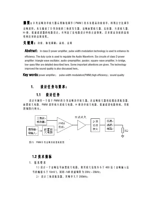
1 Performance and Reliability Improvements in High-Power Class D Audio Amplifier Design Class D Amplifiers Green energy standards, the continuing need to reduce costs and the demand for higher audio fidelity are driving the adoption of Class D amplifiers in high-power audio applications. Traditional analog implementations, such as Class AB topology, are more complex and less efficient, yet they have dominated the high-end audio market due to their high-fidelity performance. Class D systems are quickly narrowing this gap with simpler, more efficient designs offering fidelity that can surpass that of analog amplifiers. A typical Class D audio system converts audio signals at its input to a digital pulse-width modulated (PWM) signal, adds power amplification in the digital domain, then converts the digital signal back to analog at its output. As shown in Figure 1, the incoming audio signal is applied to a PWM modulator consisting of an operational amplifier and comparator. This modulator digitizes the audio input by varying the modulator duty cycle in direct proportion to the instantaneous value of the audio input signal. This PWM signal is then appropriately level-shifted and applied to a gate driver that switches a two-state power circuit consisting of MOSFETs (M1 and M2). The resulting amplified signal is then passed through an output filter, which removes the PWM carrier frequency, leaving only the amplified analog audio signal that ultimately drives the speakers. Audio output fidelity is further enhanced by the outer feedback loop from the filter input to the error amplifier input, thereby reducing distortion and noise. Figure 1: Class D Amplifier Basic Block Diagram Silicon Laboratories, Inc. Rev 0.1 2 Class D Amplifier Design Power Efficiency Historically, analog power amplifiers have relied on linear amplification circuits that are prone to high power losses. By comparison, Class D amplifier power efficiencies can be 90% or higher, depending on the design. This high efficiency benefit is intrinsic in Class D technology where binary switches (usually power MOSFETs) are the amplification mechanism. These switches are either fully on or fully off, and very little time is spent transitioning between those two states. This discrete switching action and low MOSFET on-resistance minimize I2R losses and increase efficiency. In practice, however, the switch transition time (dead time) must be long enough to avoid efficiency-killing shoot-through currents that result from both switches being on simultaneously. High Fidelity Audio fidelity can be defined as the accuracy with which sound is reproduced. For audio systems, fidelity is a proxy for the all-encompassing term “sound quality”. Various specifications are used to quantify fidelity, and while several measures are commonly used, we will focus on those that pose the greatest challenge for designers, namely Total Harmonic Distortion (THD) and Noise (N), collectively referred to as THD + N. THD is a measure of the accuracy of an audio system and is very much akin to high fidelity itself. Inaccuracies in signal reproduction create additional signal components at harmonic multiples of the input frequencies, which obviously distract from the purity of the output signal. THD is the ratio of unwanted energy from all harmonic frequencies to the energy of the fundamental frequencies of the input, typically measured at half of full power for a given system. While THD performance less than 0.1% is adequate for most non-audiophile audio applications, discerning listeners usually prefer THD levels of 0.05% or less. Output noise level is a measure of the noise floor level of the amplifier outputs with no signal input. For most speakers, a noise floor of 100-500 µV is inaudible from most normal listening distances, while a noise floor as high as 1 mV will prove to be quite annoying. Combined, THD+N is a very good measure of audio fidelity in a given amplifier. Class D Driver IC - Features and Benefits Programmable Dead-Time Class D amplifier dead- time (i.e. the period when both switches are off) directly impacts efficiency as well as THD. An overly short dead-time causes shoot-through currents that decrease efficiency; an overly long dead-time results in increased THD, which negatively affects audio fidelity. Therefore, the dead time period must be precisely set to hit the “sweet-spot” that optimizes both power efficiency and THD. The typical high-voltage audio drivers (HVICs) available today have coarse and overlapping dead time settings (i.e. 1 of n delay values); so, most designers choose to implement the dead-time period discretely, which can be expensive and time-consuming. A more elegant and cost-effective solution would be to integrate a gate driver with a highly-precise dead-time generator.