TLV3501高速比较器
- 格式:pdf
- 大小:762.10 KB
- 文档页数:21
延迟时间为4.5ns轨至轨,高速比较器Microsize软件包特点?高速:延迟时间为4.5ns?轨到轨I / O?电源电压:+2.7 V至+5.5 V?推挽式CMOS输出阶段?关闭(TLV3501只)?微套餐:采用SOT23 - 6(单人)SOT23 - 8(双)?低电源电流:3.2毫安应用?自动测试设备?无线基站?阈值检测器?过零检测器?窗口比较器TLV350x相关产品功能产品精密超高速,低功耗比较器TLC3016差分输出比较TL712高速运算放大器,16位精度,150MHz的OPA300高速运算放大器,38MHz,轨到轨OPA350OPA357 250MHz的高速运算放大器,带有关断描述推挽输出比较TLV350x家庭设有一个快速的延迟时间为4.5ns的传播延迟和操作+2.7 V至+5.5 V。
以后的护栏输入共模范围使得它为低电压应用的理想选择。
轨到轨输出,直接驱动的CMOS或TTL逻辑。
Microsize包提供了用于便携式选项空间受限的应用。
单(TLV3501)采用SOT23 - 6和SO - 8封装。
双(TLV3502)采用SOT23 - 8和SO - 8封装。
PAGE2绝对最大额定值(1)电源电压。
+5.5 V,信号输入端子,电压(2)。
(V)- 0.3V(V +)+ 0.3V信号输入端子,电流(2)。
10毫安输出短路(3)。
74毫安工作温度。
-40 °C至+125°C存储温度。
-65 °C至+150°C结温。
+150 °C铅温度(焊接,10S)。
300°C额定ESD(人体模型)。
3000V带电器件模型(CDM)。
500V(1)强调以上这些收视率可能会造成永久性损坏。
长时间暴露在绝对最大条件可能会降低设备的可靠性。
这些仅仅是极限参数,并设备的功能操作在这些或任何其他条件超出指定的那些不支持。
(2)输入端子二极管钳位的电源轨。
输入信号的摆幅可超过0.3V超出供应导轨应电流为10mA或更小有限。
tlv3502原理
TLV3502是一种低功耗、高精度的电压比较器,常用于电池供
电或低功耗应用中。
它具有双路独立比较器,可用于测量电压和电流,以及开关和电平检测等应用。
TLV3502的工作原理基于比较器
的输入电压与基准电压进行比较,从而产生高低电平输出。
其主要
特点包括低功耗、高精度、宽电压范围和快速响应等。
TLV3502采用微功耗技术,能够在低至1.8V的电压下工作,并
且具有微安级的静态电流消耗,适用于电池供电或低功耗应用。
同时,它还具有高精度的电压比较功能,能够在不同温度和电压条件
下提供稳定的输出。
其宽电压范围和快速响应特性,使得TLV3502
能够适用于各种工业控制、通信设备和便携式电子产品中。
TLV3502的工作原理是基于内部比较器对输入电压和基准电压
进行比较,并产生高低电平输出。
通过外部电路可以调节基准电压,从而实现对比较器的阈值设定。
当输入电压高于基准电压时,比较
器输出高电平;当输入电压低于基准电压时,比较器输出低电平。
这种工作原理使得TLV3502能够实现对输入信号的精确比较,并在
需要时产生相应的输出信号。
总之,TLV3502作为一种低功耗、高精度的电压比较器,具有广泛的应用前景。
其微功耗、高精度和快速响应特性,使得它能够在各种电子设备中发挥重要作用,为电压比较和开关检测提供可靠的解决方案。
TLV3501怎么做比较器,TLV3501比较器电路设计思路TLV3501 怎么做比较器,比较器电路如何设计?电压比较器(简称为比较器)是对输入信号进行鉴幅和比较的集成器件,它可将模拟信号转换成二值信号,即只有高电平和低电平两种状态的离散信号。
可用作模拟电路和数字电路的接口,也可用作波形产生和变换电路等。
比较器看起来像是开路结构中的运算放大器,但比较器和运算放大器在电气性能参数方面有许多不同之处。
运算放大器在不加负反馈时,从原理上讲可以用作比较器,但比较器的响应速度比运算放大器快,传输延迟时间比运算放大器小,而且不需外加限幅电路就可直接驱动TTL、CMOS 等数字集成电路。
但在要求不高情况下也可以考虑将某些运算放大器(例如:LM324、LM358、μA741、TL081、OP07、OP27 等)当作比较器使用。
常见的比较器电路有过零比较器、门限比较器、滞回比较器、窗口比较器和三态比较器等。
比较器的输出级主要有开路输出和推挽式输出两种输出电路结构。
(1) 集电极开路输出:集电极开路输出比较器的电路结构如集电极开路的比较器在使用时,需要外接上拉电阻R_PLL,上拉电阻与逻辑电源Vs+相连,逻辑电源的电压值,决定了比较器的可输出电压值。
采用集电极开路输出的比较器可与各种逻辑器件系列连接,并可实现线与逻辑。
(2) 集电极/发射极开路输出:集电极/发射极开路输出比较器的电路结构如集电极/发射极开路输出的比较器均需要外接上拉或下拉电阻R_PLL,采用上拉电阻与逻辑电源Vs+相连或采用下拉电阻与逻辑电源Vs-相连,逻辑电源的电压值,决定了比较器的可输出电压值。
采用集电极开路输出的比较器可与各种逻辑器件系列连接,并可实现线与逻辑。
(3) 漏极开路输出:漏极开路输出比较器的电路结构如漏极开路输出的比较器均需要外接上拉电阻R_PLL,采用上拉电阻与逻辑电源Vs+相连,逻辑电源的电压值,决定了比较器的可输出电压值。
高速电压比较器芯片一、高速电压比较器芯片的工作原理高速电压比较器芯片是一种用于比较两个输入电压大小的电子器件。
它通常由一个差分输入级、一个比较器和输出缓冲器组成。
差分输入级将两个输入电压进行差分放大,以便于比较器进行比较。
比较器根据两个输入电压的大小关系输出高低电平信号,而输出缓冲器则对比较器的输出信号进行适当的放大和缓冲,以便于驱动后级电路。
高速电压比较器芯片的工作原理主要基于比较器内部的电压传输特性。
当输入电压发生变化时,差分输入级会将其转换为差分信号,并传送到比较器的输入端。
如果输入电压达到某个阈值时,比较器将输出高电平或低电平信号。
这个阈值通常由比较器的内部电路和电源电压决定。
二、高速电压比较器芯片的性能特点高速电压比较器芯片具有以下性能特点:1.高速响应:高速电压比较器芯片通常具有快速的响应时间,可以在毫秒甚至纳秒级别内完成电压比较。
这使得它在高速模拟-数字转换器(ADC)、波形生成和采样电路等应用中具有广泛的应用。
2.精度和线性度:高速电压比较器芯片通常具有较高的精度和线性度,可以用于高精度的测量和控制系统。
此外,一些高速电压比较器芯片还具有温度补偿功能,可以减少温度对精度的影响。
3.低功耗:随着技术的发展,高速电压比较器芯片的功耗越来越低,使得它在电池供电的应用中具有更长的使用寿命。
此外,低功耗设计还可以降低散热要求,使系统更加紧凑和可靠。
4.兼容多种接口:为了满足不同的应用需求,高速电压比较器芯片可以与多种接口兼容,如SPI、I2C等。
这使得它可以与其他数字器件方便地连接和通信,从而简化了电路设计和系统集成。
5.可靠性高:高速电压比较器芯片通常具有较高的可靠性,可以在恶劣的环境条件下稳定工作。
此外,一些高速电压比较器芯片还具有过热保护、过流保护等功能,可以有效地保护系统免受过载、短路等故障的损害。
三、高速电压比较器芯片的应用场景高速电压比较器芯片在各种应用场景中都发挥着重要的作用。
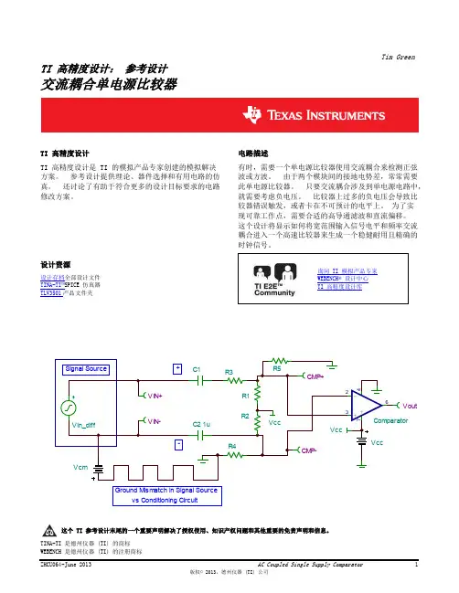
TLV3501比较器电路设计:交流耦合单电源比较器
本文为您简单介绍TLV3501 比较器-交流耦合单电源比较器设计方案,希望对您设计单电源比较器起到指导作用。
有时,需要一个单电源比较器使用交流耦合来检测正弦波或方波。
由于两个模块间的接地电势差,常常需要此单电源比较器。
只要交流耦合涉及到单电源电路中,就需要考虑负电压。
比较器上过多的负电压会导致比较器错误触发,或者卡在不可预计的电平上。
为了实现可靠工作点,需要合适的高导通滤波和直流偏移。
这个设计将显示如何将宽范围输入信号电平和频率交流耦合进入一个高速比较器来生成一个稳健耐用且精确的时钟信号。
交流耦合单电源比较器电路设计汇总
此设计需求如下:
无输入信号-比较器输出= 0V
启动时间小于1ms
电源电压:3.3V,+5%(3.135V 至3.465V)
输入信号源提供:
Vcc = 3.3V,+5%(3.135V 至3.465V)
Vcc = 5V,+5%,(4.75V 至5.25V)
输入信号电平:
VIL = GND+400mV @ Isink = 2mA
VIH = Vcc-400mV @ Isource = 2mA
共模范围:+100mV
传输延迟:5ns
占空比从输入到输出的变化10%。

TLV3501过零比较器电路设计
本文以TLV3501 过零比较器电路设计为示例,简单为您讲解过零比
较器电路设计的方法与思路,希望对您设计比较器电路有所帮助。
过零比较器电路
过零电压比较器是电压比较电路的基本结构,它可将交流信号转化为同频率的双极性矩形波。
常用于测量正弦波的频率相位等。
过零比较器电路
过零比较器电路设计方法与步骤:
下面自行设计过零电压比较器电路,反相输入端接地,同相输入端接1kHz、1V 正弦波信号,测量并绘制输出波形和电压传输特性曲线。
设计下
(1) OrCAD 仿真
扫描设置与结果如下:
为了测量上升时间,对
上升时间为0.66us
(2) 搭建电路
信号源设置如下:
观察输出波形如下:
用Measure 测量该信号的上升时间为2.4us。
TLV3501滞回比较器电路设计本文以TLV3501 滞回比较器电路设计为示例,简单为您讲解滞回比较器电路设计的方法与思路,希望对您设计比较器电路有所帮助。
什么是滞回比较器?滞回比较器:又称施密特触发器,其抗干扰能力强,如果输入电压受到干扰或噪声的影响,在门限电平上下波动,而输出电压不会在高、低两个电平间反复的跳动。
滞回比较器电路图:滞回比较器电路设计理论分析及计算:输入电压UI 经电阻R1 加在集成运放的反向输入端,参考电压UREF 经电阻R2 接在同向输入端,此外从输入端通过电阻RF 引回同向输入端。
电阻R 和背靠背稳压管VDZ 的作用是限幅,将输出电压的幅度限制在±UZ。
利用叠加原理可求得同向输入端的电位为:若原来U0=+UZ,当UI 逐渐增大时,使U0 从+UZ 跳变为-UZ 所需的门限电平用UT+表示,由上式知若原来的U0=-UZ,当UI 逐渐减小,使U0 从-UZ 跳变为+UZ 所需的门限电平用UT-表示,则由R=30kOhm,R2=20kOhm,UREF=6V,带入以上公式可以得到,UT+=5V,UT-=2V,即当UI 增大时,在UI=5V 时U0 发生跳变,而当UI 减小时,则在U0=2V 时发生跳变。
输出波形为矩形波。
滞回比较器设计仿真结果分析,如下所示:仿真分析:由RF=30kOhm,R2=20kOhm,UREF=6V,带入公式(1)(2)(3)可以得到,UT+ =5V,UT- =2V,即当UI 增大时,在UI=5V 时U0 发生跳变,而当UI 减小时,则在U0=2V 时发生跳变。
输出波形为矩形波得出结论:滞回比较器效果显著,所测得数值与理论计算数值误差在实验范围之内,是有效的实验。
tips:感谢大家的阅读,本文由我司收集整编。
仅供参阅!。

宽带前置放大电路宽带前置放大电路【摘要】:本系统设计的宽带前置放大电路由频率显示装置、输入阻抗匹配单元、无源衰减网络、有源放大电路四部分组成,带宽可达40MHz,具有良好的直流和交流特性。
频率显示部分使用TI公司的OPA842、TLV3501及MSP430F149单片机进行信号处理,使用12864液晶进行显示。
输入阻抗匹配单元有50Ω和1M Ω可选,由电阻电容组成的无源衰减网络与后级相匹配可实现不低于DC~35MHz的1倍和10倍衰减,有源放大单元选用TI公司的OPA690和OPA684可实现对信号1倍和10倍放大,电路输出电阻近似为0。
一、系统整体方案论证与比较题目要求有源放大电路采用正负5V供电,在正负5V电源及1M欧输入阻抗的条件下进行1倍、10倍衰减,以及1、10倍有源放大,可供选择方案如下:方案一:为了实现衰减和放大的功能,考虑直接选取可调增益的运放实现,如AD603。
其内部由R-2R梯形电阻网络和固定增益放大器构成,加在梯形网络输入端的信号经衰减后,由固定增益放大器输出,衰减量是由加在增益控制接口的电压决定的,优点是电路集成度高、结构简单。
缺点是此芯片的衰减量是由加在增益控制接口的参考电压决定的,要手动精准控制,难度大;梯形电阻网络的输入阻抗低,不能满足1MΩ的要求;且工作频带仅为50MHz,很难满足题目工作带宽要求。
方案二、根据题目对电路衰减和放大倍数的要求,特别是工作频带高的要求,采用宽带运放,如TI的OPA690、OPA684构成后级有源放大环节,其增益带宽积带宽均在500M以上,满足题目要求的DC~35M工作带宽的要求,1、10倍放大分开,10倍放大采用5倍与2倍相乘的形式可以降低对单级运放带宽的要求,无源衰减网络采用电阻分压构成,采用电阻分压不会限制输入信号的带宽,阻抗匹配部分采用电阻串并联形式。
综上所述:我们选择方案二作为本次比赛的总体方案。
二、系统整体框图系统整体框图如图2-1所示。
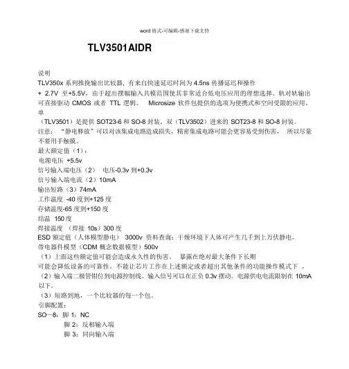
TLV3501AIDR说明TLV350x 系列推挽输出比较器, 有来自快速延迟时间为4.5ns 传播延迟和操作+ 2.7V 至+5.5V,由于超出摆幅输入共模范围使其非常适合低电压应用的理想选择。
轨对轨输出可直接驱动CMOS 或者TTL 逻辑。
Microsize 软件包提供的选项为便携式和空间受限的应用。
单(TLV3501)是提供SOT23-6 和SO-8 封装。
双(TLV3502)进来的SOT23-8 和SO-8 封装。
注意:“静电释放”可以对该集成电路造成损失,精密集成电路可能会更容易受到伤害,所以尽量不要用手触摸。
最大额定值(1):电源电压+5.5v信号输入端电压(2)电压-0.3v 到+0.3v信号输入端电流(2)10mA输出短路(3)74mA工作温度-40 度到+125 度存储温度-65 度到+150 度结温150 度焊接温度(焊接10s)300 度ESD 额定值(人体模型静电)3000v 资料查询:干燥环境下人体可产生几千到上万伏静电。
带电器件模型(CDM 概念数据模型)500v(1)上面这些额定值可能会造成永久性的伤害。
暴露在绝对最大条件下长期可能会降低设备的可靠性。
不能让芯片工作在上述额定或者超出其他条件的功能操作模式下。
(2)输入端二极管钳位到电源控制线。
输入信号可以在正负0.3v 摆动。
电源供电电流限制在10mA 以下。
(3)短路到地,一个比较器的每一个包。
引脚配置:SO—8:脚1:NC脚2:反相输入端脚3:同向输入端脚4:负电源输入端脚5:NC脚6:输出端脚7:正电源输入端脚8:关断信号控制端对于SOT23-6 封装由上图可以看出引脚1 是由定向的包装标记。
SO-8 比SOT23-6 封装多了两个NC 引脚,NC 引脚为空脚,没有内部的电路连接。
电气特性限额合用于在指定温度范围,TA = -40 °C 至+125 °C 。
普通情况下在TA=25 °C 和VS=+2.7V 至+5.5 V,除非另有说明。
高速比较器芯片型号选型表(实用版)目录1.高速比较器芯片概述2.高速比较器芯片的选型要求3.高速比较器芯片型号推荐4.总结正文一、高速比较器芯片概述高速比较器芯片是一种用于比较两个信号电压大小的电子元器件,具有响应速度快、输出波形陡峭等特点。
在高速信号处理系统中,比较器芯片起到关键作用,例如在数据通信、信号处理、振幅调制等领域。
根据不同的应用场景,高速比较器芯片有不同的性能要求,如响应速度、输入偏差、电源电压范围等。
二、高速比较器芯片的选型要求1.响应速度:高速比较器芯片的响应速度是评价其性能的重要指标。
通常情况下,响应速度越快,芯片的性能越好。
根据不同的应用场景,可选择不同响应速度的比较器芯片。
2.输入偏差:输入偏差是指比较器芯片在输入信号电压相等时,输出电压的差值。
输入偏差越小,表示比较器芯片的精度越高。
3.电源电压范围:高速比较器芯片的电源电压范围会影响其工作稳定性。
在选型时,需要根据系统电源电压范围选择合适电源电压范围的比较器芯片。
4.输出方式:高速比较器芯片的输出方式有模拟输出和数字输出两种。
模拟输出适合对信号波形要求较高的场景,数字输出则适用于需要明确信号状态的场景。
5.封装形式:高速比较器芯片的封装形式会影响其性能和稳定性。
常见的封装形式有 SOIC、TSSOP、LFCSP 等。
在选型时,需要根据实际应用场景选择合适的封装形式。
三、高速比较器芯片型号推荐根据上述选型要求,以下是几款高速比较器芯片型号推荐:1.TI 公司的 LM5017:该芯片具有快速响应速度(1ns),输入偏差低(500μV),电源电压范围宽(1.8V~5.5V),且封装形式为 LFCSP,适用于高速信号处理系统。
2.AD 公司的 ADC128S:该芯片响应速度为 2ns,输入偏差为 500μV,电源电压范围为 2.5V~5V,封装形式为 SOIC。
该芯片具有较高的性价比,适合数据通信等领域。
3.Maxim 公司的 MAX9997:该芯片具有快速响应速度(1ns),输入偏差低(500μV),电源电压范围宽(1.8V~5.5V),且封装形式为 TSSOP。
高速比较器芯片型号选型表摘要:一、高速比较器芯片概述二、高速比较器芯片型号选型表解析1.型号含义及分类2.参数解读3.应用场景及选择依据三、如何根据需求挑选合适的高速比较器芯片四、注意事项及芯片选型案例分析正文:一、高速比较器芯片概述高速比较器芯片是一种电子元器件,主要用于实现高速、高精度的信号比较功能。
在各种电子设备、仪器仪表和控制系统中有广泛的应用。
随着科技的不断发展,高速比较器芯片的性能也在不断提高,为满足各种应用场景的需求,市场上涌现出众多型号。
二、高速比较器芯片型号选型表解析1.型号含义及分类高速比较器芯片型号通常包括:制造商名称、产品系列、型号编号等。
例如,某品牌的高速比较器芯片型号为“ABC-XYZ”。
其中,制造商名称表示品牌,产品系列表示芯片的性能特点,型号编号则代表具体产品。
根据比较器芯片的工作电压、功耗、响应速度、输出信号等特点,可以将高速比较器芯片分为不同类别。
如低功耗型、高速型、高精度型等。
2.参数解读在选型表中,高速比较器芯片的参数主要包括:工作电压、输入电压范围、响应速度、输出电流、输出电压等。
这些参数决定了芯片的性能和适用范围。
例如,工作电压为3.3V的芯片适用于低电压系统,而工作电压为5V的芯片适用于较高电压系统。
3.应用场景及选择依据高速比较器芯片的应用场景包括:信号监测、频率控制、幅度调整、电平转换等。
在选择高速比较器芯片时,应根据实际应用需求,重点关注芯片的性能参数、功耗、封装尺寸等方面,确保芯片能满足系统性能要求。
三、如何根据需求挑选合适的高速比较器芯片1.确定应用场景:根据系统需求,明确比较器芯片的功能和性能要求。
2.对比参数:收集不同品牌和型号的高速比较器芯片参数,进行对比分析。
3.评估性能:针对满足需求的芯片,进一步评估其在系统中的性能表现。
4.考虑成本和封装:综合考虑芯片的成本、封装尺寸、可靠性等因素,选择性价比高的产品。
5.参考应用案例:可参考同类产品在实际应用中的表现,提高选型的准确性。
proper handling and installation procedures can cause damage. ESD damage can range from subtle performance degradation to complete device failure. Precision integrated circuits may be more susceptible to damage because very small parametric changes couldPACKAGING INFORMATIONOrderable Device Status(1)PackageType PackageDrawingPins PackageQtyEco Plan(2)Lead/Ball Finish MSL Peak Temp(3)TLV3501AID ACTIVE SOIC D875Green(RoHS&no Sb/Br)CU NIPDAU Level-2-260C-1YEARTLV3501AIDBVR ACTIVE SOT-23DBV63000Green(RoHS&no Sb/Br)CU NIPDAU Level-2-260C-1YEARTLV3501AIDBVRG4ACTIVE SOT-23DBV63000Green(RoHS&no Sb/Br)CU NIPDAU Level-2-260C-1YEARTLV3501AIDBVT ACTIVE SOT-23DBV6250Green(RoHS&no Sb/Br)CU NIPDAU Level-2-260C-1YEARTLV3501AIDBVTG4ACTIVE SOT-23DBV6250Green(RoHS&no Sb/Br)CU NIPDAU Level-2-260C-1YEARTLV3501AIDG4ACTIVE SOIC D875Green(RoHS&no Sb/Br)CU NIPDAU Level-2-260C-1YEARTLV3501AIDR ACTIVE SOIC D82500Green(RoHS&no Sb/Br)CU NIPDAU Level-2-260C-1YEARTLV3501AIDRG4ACTIVE SOIC D82500Green(RoHS&no Sb/Br)CU NIPDAU Level-2-260C-1YEARTLV3502AID ACTIVE SOIC D875Green(RoHS&no Sb/Br)CU NIPDAU Level-2-260C-1YEARTLV3502AIDCNR ACTIVE SOT-23DCN83000Green(RoHS&no Sb/Br)CU NIPDAU Level-2-260C-1YEARTLV3502AIDCNRG4ACTIVE SOT-23DCN83000Green(RoHS&no Sb/Br)CU NIPDAU Level-2-260C-1YEARTLV3502AIDCNT ACTIVE SOT-23DCN8250Green(RoHS&no Sb/Br)CU NIPDAU Level-2-260C-1YEARTLV3502AIDCNTG4ACTIVE SOT-23DCN8250Green(RoHS&no Sb/Br)CU NIPDAU Level-2-260C-1YEARTLV3502AIDG4ACTIVE SOIC D875Green(RoHS&no Sb/Br)CU NIPDAU Level-2-260C-1YEARTLV3502AIDR ACTIVE SOIC D82500Green(RoHS&no Sb/Br)CU NIPDAU Level-2-260C-1YEARTLV3502AIDRG4ACTIVE SOIC D82500Green(RoHS&no Sb/Br)CU NIPDAU Level-2-260C-1YEAR(1)The marketing status values are defined as follows:ACTIVE:Product device recommended for new designs.LIFEBUY:TI has announced that the device will be discontinued,and a lifetime-buy period is in effect.NRND:Not recommended for new designs.Device is in production to support existing customers,but TI does not recommend using this part in a new design.PREVIEW:Device has been announced but is not in production.Samples may or may not be available.OBSOLETE:TI has discontinued the production of the device.(2)Eco Plan-The planned eco-friendly classification:Pb-Free(RoHS),Pb-Free(RoHS Exempt),or Green(RoHS&no Sb/Br)-please check /productcontent for the latest availability information and additional product content details.TBD:The Pb-Free/Green conversion plan has not been defined.Pb-Free(RoHS):TI's terms"Lead-Free"or"Pb-Free"mean semiconductor products that are compatible with the current RoHS requirements for all6substances,including the requirement that lead not exceed0.1%by weight in homogeneous materials.Where designed to be soldered at high temperatures,TI Pb-Free products are suitable for use in specified lead-free processes.Pb-Free(RoHS Exempt):This component has a RoHS exemption for either1)lead-based flip-chip solder bumps used between the die and package,or2)lead-based die adhesive used between the die and leadframe.The component is otherwise considered Pb-Free(RoHS compatible)as defined above.Green(RoHS&no Sb/Br):TI defines"Green"to mean Pb-Free(RoHS compatible),and free of Bromine(Br)and Antimony(Sb)based flame retardants(Br or Sb do not exceed0.1%by weight in homogeneous material)(3)MSL,Peak Temp.--The Moisture Sensitivity Level rating according to the JEDEC industry standard classifications,and peak solder temperature.Important Information and Disclaimer:The information provided on this page represents TI's knowledge and belief as of the date that it is provided.TI bases its knowledge and belief on information provided by third parties,and makes no representation or warranty as to the accuracy of such information.Efforts are underway to better integrate information from third parties.TI has taken and continues to take reasonable steps to provide representative and accurate information but may not have conducted destructive testing or chemical analysis on incoming materials and chemicals.TI and TI suppliers consider certain information to be proprietary,and thus CAS numbers and other limited information may not be available for release.In no event shall TI's liability arising out of such information exceed the total purchase price of the TI part(s)at issue in this document sold by TI to Customer on an annual basis.OTHER QUALIFIED VERSIONS OF TLV3502:•Automotive:TLV3502-Q1NOTE:Qualified Version Definitions:•Automotive-Q100devices qualified for high-reliability automotive applications targeting zero defectsTAPE AND REEL INFORMATION*All dimensions are nominal Device Package Type Package DrawingPinsSPQ Reel Diameter (mm)Reel Width W1(mm)A0(mm)B0(mm)K0(mm)P1(mm)W (mm)Pin1Quadrant TLV3501AIDBVR SOT-23DBV 63000180.08.4 3.2 3.1 1.39 4.08.0Q3TLV3501AIDBVT SOT-23DBV 6250180.08.4 3.2 3.1 1.39 4.08.0Q3TLV3501AIDR SOICD 82500330.012.4 6.4 5.2 2.18.012.0Q1TLV3502AIDCNR SOT-23DCN 83000179.08.4 3.2 3.2 1.4 4.08.0Q3TLV3502AIDCNT SOT-23DCN 8250179.08.4 3.2 3.2 1.4 4.08.0Q3TLV3502AIDR SOIC D 82500330.012.4 6.4 5.2 2.18.012.0Q1*All dimensions are nominalDevice Package Type Package Drawing Pins SPQ Length(mm)Width(mm)Height(mm) TLV3501AIDBVR SOT-23DBV63000190.5212.731.8 TLV3501AIDBVT SOT-23DBV6250190.5212.731.8 TLV3501AIDR SOIC D8*******.0346.029.0 TLV3502AIDCNR SOT-23DCN83000195.0200.045.0 TLV3502AIDCNT SOT-23DCN8250195.0200.045.0 TLV3502AIDR SOIC D8*******.0346.029.0IMPORTANT NOTICETexas Instruments Incorporated and its subsidiaries(TI)reserve the right to make corrections,modifications,enhancements,improvements, and other changes to its products and services at any time and to discontinue any product or service without notice.Customers should obtain the latest relevant information before placing orders and should verify that such information is current and complete.All products are sold subject to TI’s terms and conditions of sale supplied at the time of order acknowledgment.TI warrants performance of its hardware products to the specifications applicable at the time of sale in accordance with TI’s standard warranty.Testing and other quality control techniques are used to the extent TI deems necessary to support this warranty.Except where mandated by government requirements,testing of all parameters of each product is not necessarily performed.TI assumes no liability for applications assistance or customer product design.Customers are responsible for their products and applications using TI components.To minimize the risks associated with customer products and applications,customers should provide adequate design and operating safeguards.TI does not warrant or represent that any license,either express or implied,is granted under any TI patent right,copyright,mask work right, or other TI intellectual property right relating to any combination,machine,or process in which TI products or services are rmation published by TI regarding third-party products or services does not constitute a license from TI to use such products or services or a warranty or endorsement e of such information may require a license from a third party under the patents or other intellectual property of the third party,or a license from TI under the patents or other intellectual property of TI.Reproduction of TI information in TI data books or data sheets is permissible only if reproduction is without alteration and is accompanied by all associated warranties,conditions,limitations,and notices.Reproduction of this information with alteration is an unfair and deceptive business practice.TI is not responsible or liable for such altered rmation of third parties may be subject to additional restrictions.Resale of TI products or services with statements different from or beyond the parameters stated by TI for that product or service voids all express and any implied warranties for the associated TI product or service and is an unfair and deceptive business practice.TI is not responsible or liable for any such statements.TI products are not authorized for use in safety-critical applications(such as life support)where a failure of the TI product would reasonably be expected to cause severe personal injury or death,unless officers of the parties have executed an agreement specifically governing such use.Buyers represent that they have all necessary expertise in the safety and regulatory ramifications of their applications,and acknowledge and agree that they are solely responsible for all legal,regulatory and safety-related requirements concerning their products and any use of TI products in such safety-critical applications,notwithstanding any applications-related information or support that may be provided by TI.Further,Buyers must fully indemnify TI and its representatives against any damages arising out of the use of TI products in such safety-critical applications.TI products are neither designed nor intended for use in military/aerospace applications or environments unless the TI products are specifically designated by TI as military-grade or"enhanced plastic."Only products designated by TI as military-grade meet military specifications.Buyers acknowledge and agree that any such use of TI products which TI has not designated as military-grade is solely at the Buyer's risk,and that they are solely responsible for compliance with all legal and regulatory requirements in connection with such use. TI products are neither designed nor intended for use in automotive applications or environments unless the specific TI products are designated by TI as compliant with ISO/TS16949requirements.Buyers acknowledge and agree that,if they use any non-designated products in automotive applications,TI will not be responsible for any failure to meet such requirements.Following are URLs where you can obtain information on other Texas Instruments products and application solutions:Products ApplicationsAudio /audio Communications and Telecom /communicationsAmplifiers Computers and Peripherals /computersData Converters Consumer Electronics /consumer-appsDLP®Products Energy and Lighting /energyDSP Industrial /industrialClocks and Timers /clocks Medical /medicalInterface Security /securityLogic Space,Avionics and Defense /space-avionics-defense Power Mgmt Transportation and /automotiveAutomotiveMicrocontrollers Video and Imaging /videoRFID Wireless /wireless-appsRF/IF and ZigBee®Solutions /lprfTI E2E Community Home Page Mailing Address:Texas Instruments,Post Office Box655303,Dallas,Texas75265Copyright©2011,Texas Instruments Incorporated。
数电课设报告姓名:郑中权学号:152210303127班级:电子1班江苏科技大学2017/10/12100MHz等精度频率计设计(基于Verilog HDL)一、设计要求:提供一个幅值为10mV ~ 1 V,频率为 1 ~ 100MHz的正弦信号,需测试以下指标:1.频率:测频范围 1Hz ~ 100MHz,测频精度为测频全域内相对误差恒为百万分之一。
2.占空比:测试精度 1% ~ 99%3.相位差:测试两个同频率的信号之间的相位差,测试范围 0 ~ 360二、设计分析使用FPGA数字信号处理方法,首先需要将正弦信号转换成可读取的数字方波信号,再经过FPGA设计计算得出所需测量值。
三、模电部分首先选择比较器,对于 100 MHz 信号,比较器灵敏度需要达到5ns内,TI公司的LTV3501灵敏度为4.5ns,符合要求由TLV3501数据手册得知:当频率低于 50MHz 的时候,正弦波的峰峰值需大于 20mV,频率高于50MHz 时,峰峰值需大于 1V。
然后需要选择放大器,当正弦波幅值为 10mV时,放大倍数需大于35。
方法通过二级放大,一级用OPA847放大20倍,二级用OPA675放大8倍,得到总放大倍数160的正弦波。
经转换后的输出电压符合TTL电平要求,可以被识别出0和1。
四、数电部分开发板:Cyclone IV E: EP4CE6E22C8板载时钟为 50MHz,带4个按键和一个复位键(按键按下为0,抬起为1),四个七段数码管(共阳),FPGA的引脚可由杜邦线引出。
设计思路:测量频率:输入一个100MHz的基准频率,由计数器CNT1来计算基准频率的上升沿个数,即周期数。
输入一个被测信号,它由计数器CNT2来测量周期数。
两个信号在同一个使能信号EN(使能信号时间为1~2s)下开始计数,计数完后,存储计数结果,由(CNT1 * 10)可以算出具体的计数时间(单位ns),再由((CNT1 * 10ns)/CNT2 )*10^9可算得被测信号频率,单位Hz。
proper handling and installation procedures can cause damage. ESD damage can range from subtle performance degradation to complete device failure. Precision integrated circuits may be more susceptible to damage because very small parametric changes couldPACKAGING INFORMATION(1)The marketing status values are defined as follows:ACTIVE:Product device recommended for new designs.LIFEBUY:TI has announced that the device will be discontinued,and a lifetime-buy period is in effect.NRND:Not recommended for new designs.Device is in production to support existing customers,but TI does not recommend using this part in a new design.PREVIEW:Device has been announced but is not in production.Samples may or may not be available.OBSOLETE:TI has discontinued the production of the device.(2)Eco Plan-The planned eco-friendly classification:Pb-Free(RoHS),Pb-Free(RoHS Exempt),or Green(RoHS&no Sb/Br)-please check /productcontent for the latest availability information and additional product content details.TBD:The Pb-Free/Green conversion plan has not been defined.Pb-Free(RoHS):TI's terms"Lead-Free"or"Pb-Free"mean semiconductor products that are compatible with the current RoHS requirements for all6substances,including the requirement that lead not exceed0.1%by weight in homogeneous materials.Where designed to be soldered at high temperatures,TI Pb-Free products are suitable for use in specified lead-free processes.Pb-Free(RoHS Exempt):This component has a RoHS exemption for either1)lead-based flip-chip solder bumps used between the die and package,or2)lead-based die adhesive used between the die and leadframe.The component is otherwise considered Pb-Free(RoHS compatible)as defined above.Green(RoHS&no Sb/Br):TI defines"Green"to mean Pb-Free(RoHS compatible),and free of Bromine(Br)and Antimony(Sb)based flame retardants(Br or Sb do not exceed0.1%by weight in homogeneous material)(3)MSL,Peak Temp.--The Moisture Sensitivity Level rating according to the JEDEC industry standard classifications,and peak solder temperature.Important Information and Disclaimer:The information provided on this page represents TI's knowledge and belief as of the date that it is provided.TI bases its knowledge and belief on information provided by third parties,and makes no representation or warranty as to the accuracy of such information.Efforts are underway to better integrate information from third parties.TI has taken and continues to take reasonable steps to provide representative and accurate information but may not have conducted destructive testing or chemical analysis on incoming materials and chemicals.TI and TI suppliers consider certain information to be proprietary,and thus CAS numbers and other limited information may not be available for release.In no event shall TI's liability arising out of such information exceed the total purchase price of the TI part(s)at issue in this document sold by TI to Customer on an annual basis.OTHER QUALIFIED VERSIONS OF TLV3502:•Automotive:TLV3502-Q1NOTE:Qualified Version Definitions:•Automotive-Q100devices qualified for high-reliability automotive applications targeting zero defectsTAPE AND REEL INFORMATION*All dimensions are nominal Device Package Type Package DrawingPinsSPQ Reel Diameter (mm)Reel Width W1(mm)A0(mm)B0(mm)K0(mm)P1(mm)W (mm)Pin1Quadrant TLV3501AIDBVR SOT-23DBV 63000180.08.4 3.2 3.1 1.39 4.08.0Q3TLV3501AIDBVT SOT-23DBV 6250180.08.4 3.2 3.1 1.39 4.08.0Q3TLV3501AIDR SOICD 82500330.012.4 6.4 5.2 2.18.012.0Q1TLV3502AIDCNR SOT-23DCN 83000179.08.4 3.2 3.2 1.4 4.08.0Q3TLV3502AIDCNT SOT-23DCN 8250179.08.4 3.2 3.2 1.4 4.08.0Q3TLV3502AIDR SOIC D 82500330.012.4 6.4 5.2 2.18.012.0Q1*All dimensions are nominalDevice Package Type Package Drawing Pins SPQ Length(mm)Width(mm)Height(mm) TLV3501AIDBVR SOT-23DBV63000190.5212.731.8 TLV3501AIDBVT SOT-23DBV6250190.5212.731.8 TLV3501AIDR SOIC D8*******.0346.029.0 TLV3502AIDCNR SOT-23DCN83000195.0200.045.0 TLV3502AIDCNT SOT-23DCN8250195.0200.045.0 TLV3502AIDR SOIC D8*******.0346.029.0IMPORTANT NOTICETexas Instruments Incorporated and its subsidiaries(TI)reserve the right to make corrections,modifications,enhancements,improvements, and other changes to its products and services at any time and to discontinue any product or service without notice.Customers should obtain the latest relevant information before placing orders and should verify that such information is current and complete.All products are sold subject to TI’s terms and conditions of sale supplied at the time of order acknowledgment.TI warrants performance of its hardware products to the specifications applicable at the time of sale in accordance with TI’s standard warranty.Testing and other quality control techniques are used to the extent TI deems necessary to support this warranty.Except where mandated by government requirements,testing of all parameters of each product is not necessarily performed.TI assumes no liability for applications assistance or customer product design.Customers are responsible for their products and applications using TI components.To minimize the risks associated with customer products and applications,customers should provide adequate design and operating safeguards.TI does not warrant or represent that any license,either express or implied,is granted under any TI patent right,copyright,mask work right, or other TI intellectual property right relating to any combination,machine,or process in which TI products or services are rmation published by TI regarding third-party products or services does not constitute a license from TI to use such products or services or a warranty or endorsement e of such information may require a license from a third party under the patents or other intellectual property of the third party,or a license from TI under the patents or other intellectual property of TI.Reproduction of TI information in TI data books or data sheets is permissible only if reproduction is without alteration and is accompanied by all associated warranties,conditions,limitations,and notices.Reproduction of this information with alteration is an unfair and deceptive business practice.TI is not responsible or liable for such altered rmation of third parties may be subject to additional restrictions.Resale of TI products or services with statements different from or beyond the parameters stated by TI for that product or service voids all express and any implied warranties for the associated TI product or service and is an unfair and deceptive business practice.TI is not responsible or liable for any such statements.TI products are not authorized for use in safety-critical applications(such as life support)where a failure of the TI product would reasonably be expected to cause severe personal injury or death,unless officers of the parties have executed an agreement specifically governing such use.Buyers represent that they have all necessary expertise in the safety and regulatory ramifications of their applications,and acknowledge and agree that they are solely responsible for all legal,regulatory and safety-related requirements concerning their products and any use of TI products in such safety-critical applications,notwithstanding any applications-related information or support that may be provided by TI.Further,Buyers must fully indemnify TI and its representatives against any damages arising out of the use of TI products in such safety-critical applications.TI products are neither designed nor intended for use in military/aerospace applications or environments unless the TI products are specifically designated by TI as military-grade or"enhanced plastic."Only products designated by TI as military-grade meet military specifications.Buyers acknowledge and agree that any such use of TI products which TI has not designated as military-grade is solely at the Buyer's risk,and that they are solely responsible for compliance with all legal and regulatory requirements in connection with such use. TI products are neither designed nor intended for use in automotive applications or environments unless the specific TI products are designated by TI as compliant with ISO/TS16949requirements.Buyers acknowledge and agree that,if they use any non-designated products in automotive applications,TI will not be responsible for any failure to meet such requirements.Following are URLs where you can obtain information on other Texas Instruments products and application solutions:Products ApplicationsAudio /audio Communications and Telecom /communicationsAmplifiers Computers and Peripherals /computersData Converters Consumer Electronics /consumer-appsDLP®Products Energy and Lighting /energyDSP Industrial /industrialClocks and Timers /clocks Medical /medicalInterface Security /securityLogic Space,Avionics and Defense /space-avionics-defense Power Mgmt Transportation and /automotiveAutomotiveMicrocontrollers Video and Imaging /videoRFID Wireless /wireless-appsRF/IF and ZigBee®Solutions /lprfTI E2E Community Home Page Mailing Address:Texas Instruments,Post Office Box655303,Dallas,Texas75265Copyright©2011,Texas Instruments Incorporated。