Comparative Study of DSP Techniques for the Effective Modeling and Design of Highly Complex
- 格式:pdf
- 大小:399.61 KB
- 文档页数:4

浅谈“亮考帮”与对分易平台相结合的作业模式的实践与应用发布时间:2021-09-07T09:57:24.273Z 来源:《中小学教育》2021年第5月第12期作者:史剑峰[导读] “亮考帮”是对分课堂教学下的作业模式,而“对分易”平台是一个普适性的教学平台,是对分课堂的官方教学平台。
史剑峰佛山市顺德胡锦超职业技术学校广东省佛山市 528300【摘要】 “亮考帮”是对分课堂教学下的作业模式,而“对分易”平台是一个普适性的教学平台,是对分课堂的官方教学平台。
在高职高考英语备考过程中,把“亮考帮”作业模式和对分易平台作业模式结合使用,以更好地提高学生的作业质量,效率与效果,对互联网+教学的模式进行实践应用。
【关键词】对分课堂;“亮考帮”;对分易平台;实践应用一、对分课堂与“亮考帮”2014年普林斯顿心理学博士,复旦心理系学科带头人张学新教授首次提出一种具有原创意义、本土化的新型教学模式——“对分课堂”。
“对分课堂”形式上把课堂时间一分为二,一半留给教师讲授,一半留给学生进行讨论,是一个输入(presentation)-内化(assimilation)-输出(discussion)的学习过程,简称PAD,实质上在讲授和讨论之间引入一个心理学的内化环节,让学生对讲授内容进行吸收之后,有备而来参与讨论,通过对讲授与讨论的有机整合,实现了教法与学法的对立统一。
对分课堂的一个作业特色是“亮考帮”,它是对分易教学中的一个主要作业形式。
“亮闪闪”中列出学生感受最深,受益最大的内容,是学生学习的心得;“考考你”中列出自己已经掌握,但觉得其他同学可能困惑的知识点;“帮帮我”中列出自己还不懂的知识点,在课堂讨论时寻求帮助。
“亮考帮”的设计,关注了学生不同的学习要求,是学生思考问题、提出问题、解决问题的过程。
亮考帮的作业模式不仅能体现学生是否全面参与课堂活动,也能体现同学在复习内化讨论环节的态度,以及对待学习的态度,在高职英语高考备考课堂教学实践中有重要的作用。
最新的继电保护外文精选英语参考文献最新的继电保护外文精选英语参考文献本文关键词:外文,英语,参考文献,继电保护,精选最新的继电保护外文精选英语参考文献本文简介:对于很多研究继电保护这一专业的学生们来说,参考文献的选择尤其重要,参考文献主要考察的就是同学们对这行业的研究水平以及掌握的知识范围,现为方便广大此专业的学生们,今学术堂统计整理了部分最新的继电保护的英语参考文献,希望可以帮助到大家。
继电保护英语参考文献一:[1]AbhishekKhanna.最新的继电保护外文精选英语参考文献本文内容:对于很多研究继电保护这一专业的学生们来说,参考文献的选择尤其重要,参考文献主要考察的就是同学们对这行业的研究水平以及掌握的知识范围,现为方便广大此专业的学生们,今学术堂统计整理了部分最新的继电保护的英语参考文献,希望可以帮助到大家。
继电保护英语参考文献一:[1]Abhishek Khanna. Analysis of High Impedance Protection Considering CT-Transients and Air Gapped CTs with Setting Recommendations and a New Fast Acting Algorithm for High Impedance Numerical Relays[J]. International Journal of Emerging Electric Power Systems,20xx,12(1):. [2]Mojtaba Khederzadeh. Mechanical Protection of Induction Motors by Off-the-Shelf Electrical Protective Relays[J]. International Journal of Emerging Electric Power Systems,20xx,12(2):.[3]El Sayed M. Tag Eldin. A Novel Approach for Classifying Transient Phenomena in Power Transformers[J]. International Journal of Emerging Electric Power Systems,20xx,1(2):. [4]J. Havelka,R. Malari?,K. Frlan. Staged-Fault Testing of Distance Protection Relay Settings[J]. Measurement Science Review,20xx,12(3):. [5]Xiong Haijun,Zhang Qi.A New Method for Setting Calculation Sequence of Directional Relay Protection in Multi-Loop Networks[J]. International Journal of Emerging Electric Power Systems,20xx,17(4):. [6]Si Tuyou,Wu Jiekang,Yuan Weideng,Du Anan. Power supply risk assessment method for relay protectionsystem faults[J]. Archives of Electrical Engineering,20xx,65(4):.[7]Elmer Sorrentino. Analysis of overtravel in induction disc overcurrent relays[J]. Electric Power Systems Research,20xx,:.[8]Stanislav Misak,Jindrich Stuchly,Jakub Vramba,Tomas Vantuch,David Seidl. A novel approach to adaptive active relay protection system in single phase AC coupling Off-Grid systems[J]. Electric Power Systems Research,20xx,131:.[9]Rahul Dubey,S.R. Samantaray,B.K. Panigrahi. Data-mining model based adaptive protection scheme to enhance distance relay performance during power swing[J]. International Journal of Electrical Power and Energy Systems,20xx,:. [10]Manoj Thakur,Anand Kumar. Optimal coordination of directional over current relays using a modified real coded genetic algorithm: A comparative study[J]. International Journal of Electrical Power and Energy Systems,20xx,:. [11]Miodrag Forcan,Zoran Stojanovi?. An algorithm for sensitive directional transverse differential protection with no voltage inputs[J]. Electric Power Systems Research,20xx,:.[12]Oleg Sivov,Hany Abdelsalam,Elham Makram. Adaptive setting of distance relay for MOV-protected series compensated line considering wind power[J]. Electric Power Systems Research,20xx,:.[13]S.A. Ahmadi,H. Karami,M.J. Sanjari,H. Tarimoradi,G.B. Gharehpetian. Application of Hyper-Spherical Search Algorithm for Optimal Coordination of Overcurrent Relays Considering Different Relays Characteristics[J]. International Journal of Electrical Power and Energy Systems,20xx,:.[14]Ahmed R. Adly,Ragab A. El Sehiemy,Almoataz Y. Abdelaziz. A negative sequence superimposed pilot protection technique during single pole tripping[J]. Electric Power Systems Research,20xx,:.[15]L.A. Trujillo Guajardo. Prony filter vs conventional filters for distance protection relays: An evaluation[J]. Electric Power Systems Research,20xx,:. [16]Zohaib Akhtar,Muhammad Asghar Saqib. Microgrids formed by renewable energy integration into power grids pose electricalprotection challenges[J]. Renewable Energy,20xx,:.[17]A.M. Ibrahim,W. Elkhatam,M. Mesallamy,H.A. Talaat. Adaptive Protection Coordination Scheme For Distribution Network with Distributed Generation using ABC[J]. Journal of Electrical Systems and Information Technology,20xx,:.[18]Ricardo C. Santos,Simon Le Blond,Denis V. Coury,Raj K. Aggarwal. A novel and comprehensive single terminal ANN based decision support for relaying of VSC based HVDC links[J]. Electric Power Systems Research,20xx,:.[19]Meng Yen Shih,Arturo Conde Enríquez,Tsun-Yu Hsiao,Luis Martín Torres Trevi?o. Enhanced differential evolution algorithm for coordination of directional overcurrent relays[J]. Electric Power Systems Research,20xx,:.[20]Fernando B. Bottura,Wellington M.S. Bernardes,Mário Olesko vicz,Eduardo N. Asada. Setting Directional Overcurrent Protection Parameters using Hybrid GA Optimizer[J]. Electric Power Systems Research,20xx,:.[21]Mazen Abdel-Salam,Rashad Kamel,Khairy Sayed,Mohsen Khalaf. Design and implementation of a multifunction DSP-based-numerical relay[J]. Electric Power Systems Research,20xx,143:. [22]Elmer Sorrentino. Behavior of induction disc overcurrent relays as a function of the frequency[J]. Electric Power Systems Research,20xx,:. [23]Emilio C. Piesciorovsky,Noel N. Schulz. Comparison of Non-Real-Time and Real-Time Simulators with Relays In-The-Loop for Adaptive Overcurrent Protection[J]. Electric Power Systems Research,20xx,:.[24]Akbar Sharafi,Majid Sanaye-Pasand,Farrokh Aminifar. Transmission System Wide-area Back-up Protection using Current Phasor Measurements[J]. International Journal of Electrical Power and Energy Systems,20xx,:. [25]Min Zhu,Wei Dong Liu,Wen Song Hu. Application of Fuzzy Neural Network in Relay Protection[J]. Advanced Materials Research,20xx,1100(181):. [26]Wei Kang,Xing Chen,Jian Ting Gui,He Zhang,Li Xia Zhang. Research onMicrocomputer Relay Protection Anti-Interference of 500kV Transmission Line in MATLAB[J]. Advanced Materials Research,20xx,1158(204):.[27]Wei Ming Guo,Gan Qing Zuo,Rui Lin. The Analysis of the Opto-Couplers Relay Malfunctions in HVDC Control and Protection and the Improvements of the Trip Circuits[J]. Advanced Materials Research,20xx,1478(354):.[28]Shi Qi Liu,Huan Wang,Xiao Ming Li,Dong Xu Zhou. The Research on High-Voltage Transmission Line Relay Protection Setting Related to OLTC Anti-Icing[J]. Advanced Materials Research,20xx,1518(383):.[29]Xiao Ming Li,Sha Li,Peng Lu,Shu Qiong Liu. The Study on Configuration and Setting of Relay Protection when Distributed Generation Accesses to Distribution Network[J]. Advanced Materials Research,20xx,1566(433):.[30]Shi En He,Xin Zhou Dong,Zhi Qian Bo,Jia Le Suo Nan. The Relay Protection Scheme for Distribution Network with Distributed Generations[J]. Advanced Materials Research,20xx,1566(433):.附件下载:123下一页。

ISSN 1002-4956 CN11-2034/T实验技术与管理Experimental Technology and Management第37卷第7期2020年7月Vol.37No.7Jul.2020DOI: 10.16791/ki.sjg.2020.07.039“新工科”背景下“D SP技术”课程教学改革与实践曹洪龙,胡剑凌,邵雷,李娟娟,姜敏(苏州大学电子信息学院,江苏苏州215006 )摘要:以“D SP技术”课程教学为例,从教学内容设计、教学方法改革和过程化考核三方面探索了“新工 科”背景下“D SP技术”课程教学改革的实践。
该教学改革包括以问题为导向、采用思维导图和案例教学方法、利用“面授+网络”混合教学模式和过程化考核方法等,大大提高了课程教学质量。
关键词:新工科;混合教学;过程化考核;DSP技术中图分类号:G420 文献标识码: A 文章编号:1002-4956(2020)07-0173-03Teaching reform and practice of “DSP technology”under background o f‘‘New engineering”C A O H o n g l o n g,H U Jianling,S H A O Lei,LI Juanjuan,J I A N G M i n(School of Electronic Information, Soochow University, Suzhou 215006, China)Abstract: By taking the teaching of “DSP technology” as an example, this paper explores upon the practice of teaching reform of “DSP technology” under the background of “New engineering” from three aspects of teaching content design, teaching method reform and process assessment. This teaching reform includes the problem- oriented, mind-mapping and case-teaching methods, face-to-face + network hybrid teaching model and process assessment method, which improves the teaching quality of the course.Key words: new engineering; hybrid teaching; process assessment; DSP technology随着大数据、人工智能(A I )等前沿科技的高速 发展,激发了新一轮科技革命和产业变革浪潮,也给 高等工程教育带来了新的机遇与挑战[1]。
基于DSP的歌曲伴奏(人声)提取随着互联网的普及和多媒体技术的飞速发展,网络上的音乐数量呈现了爆炸式的增长。
与此同时越来越多的用户开始使用网络音乐应用,带来了多样化的音乐信息需求。
因此,如何自动地对海量音乐数据进行有效的组织和管理,以及如何从音乐中提取各种不同的信息成为了亟待解决的问题。
声音处理是BJTU_DSP5502实验板的重要应用,也是音乐信息检索的重要内容。
基于时间或频率的声音分析带给人们许多便捷。
歌曲包含了真实人声和伴奏背景音乐,是一个复杂的音源。
由于歌曲是时域人体声带发声和演奏器具发声的混合叠加,音源之间相关性不大,因此使用软件和硬件结合的方法分离人声和伴奏音是可行的。
近年来,有很多针对演唱者识别的研究,但是效果有限,通过歌唱人声分离算法的辅助,能大幅度提高识别精度。
另外,分离出来的人声内容还可以应用在歌唱教学软件,它能对比流行歌曲中的人声演唱部分和用户录音,分析用户的表达精准度,自动给用户打分。
分离出的人声也可以用于后续的语音识别处理,伴奏音分离之后可用于娱乐,也可以作为乐队(伴奏系统)的评价和技术分析。
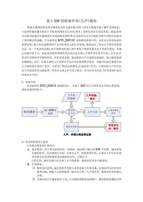
1、实验目的本实验利用BJTU_DSP550实验板设计一个基于DSP的人声和伴奏音乐的分离系统。
系统实现结构如下:人声、伴奏分离处理过程2、技术指标和设计要求分为基本要求和扩展部分:A.基本要求:对于事先录制好的一段歌曲,通过接口输入到DSP开发板,通过实现存储的程序,对音频进行分析,分离出人声,得到背景伴奏。
分离出人声后伴奏或者背景音乐必须保留原有的旋律和音色,不能有太大的失真。
最后存储已经分离了人声的歌曲,歌曲的长度亦不能缩短。
B.扩展要求:1)能够实时处理。
通过连接开发板与采集设备与存储设备。
实现短时间内的实时处理功能。
即输入为原始歌曲,输出为分离了人声的伴奏,能够实时监听输出音频。
2)分离出的人声能够保存下来。
并且能够消除附加的噪声,最终能够清楚地分辨出人声并且保持连贯。
通过分析,可以得到歌声基因的基本参数。


基于MLSE的新型分数间隔均衡研究周小林;毕伟祥;赵鑫【摘要】针对GMSK调制通信系统中,传统MLSE均衡技术存在的对定时偏差较为敏感的问题,给出一种新型的分数间隔均衡方案.该方案的算法结构并不是传统的匹配滤波加白化滤波器的结构,而是基于改进型Viterbi算法(MVA).该方案较好地解决了传统MLSE均衡对定时偏差敏感的问题.仿真分析表明,相比于传统的MLSE 均衡,所提出的分数间隔均衡方案可以有效地改善均衡效果,同时在同频干扰下性能优良.【期刊名称】《上海师范大学学报(自然科学版)》【年(卷),期】2015(044)005【总页数】5页(P528-532)【关键词】MLSE;分数间隔均衡;定时偏差;MVA【作者】周小林;毕伟祥;赵鑫【作者单位】复旦大学信息科学与工程学院,上海200433;复旦大学信息科学与工程学院,上海200433;复旦大学信息科学与工程学院,上海200433【正文语种】中文【中图分类】TN929.5在GGE通信系统中,使用最多的均衡方式是基于维特比译码的最大似然序列估计MLSE,以对抗信道带来的衰落[1].在加性白高斯噪声(AWGN)条件下,MLSE算法在使序列差错概率最小化的意义上是最优的.但是,传统的基于符号间隔的MLSE均衡器容易受定时偏差的影响[2],为了减小定时偏差带来的影响,本文作者将常规线性均衡器中采用分数间隔抽样来减少定时偏差影响的办法[3]应用于MLSE均衡器.对于传统的MLSE均衡器,Forney最早提出了采用Viterbi算法(VA)实现最大似然序列估计的接收机结构[4].该接收机由匹配滤波器、白化滤波器和VA检测器组成.高斯白噪声经过匹配滤波器之后变为了有色噪声,所以需要进行白化滤波,使采样点上的噪声分量统计独立.不过,由于白化滤波器在实现中比较复杂,Ungerboeck便提出了采用改进型Viterbi算法(MVA)的接收机结构[5],该结构中MVA算法考虑到了噪声样点的相关性,量度的递归计算直接在匹配滤波器输出的样值序列上进行,不需要白化滤波器[6-7],而且MVA的度量值运算中没有VA算法中的平方操作,复杂度显著降低.Hamied和Gordon于1995年提出基于分数间隔采样的MLSE均衡器[8],该均衡器性能上与符号间隔采样相同,同时对定时偏差不敏感.但该均衡器结构与Forney提出的均衡器结构相同,使用了白化滤波器,而白化滤波器在实际应用中并不容易实现.后续基于分数间隔采样的研究基本上也都没有脱离白化滤波器.本文作者提出的分数间隔均衡器则不同以往,其是以Ungerboeck均衡器结构为基础,在接收机结构和复杂度上都优于带有白化滤波器的分数间隔均衡器.文章结构为:第1章具体介绍所设计的新型分数间隔均衡器的算法模型,第2章给出该算法的仿真结果及其相关的分析.最后第3章给出总结.如图1所示,设计的接收机结构主要包括信道估计(Channel Estimation)、匹配滤波(Matched Filter)以及分数间隔MAV检测器(T/2-spaced MVA).实际应用中均衡算法处理的是数字信号,因此接收的模拟信号r(t)(已经下变频为基带的信号)在进入均衡之前需要进行分数间隔采样,采样之后的数据可以等效成两路符号间隔的信号[9]与,分别经过信道估计和匹配滤波处理,将滤波后的两路信号与送入分数间隔MVA检测器最后输出估计序列{}.信道估计模块可以使用传统的自适应估计器,本方案中采用LMS信道估计器.接下来分别对匹配滤波以及分数间隔MVA检测器的算法进行具体说明.1.1 匹配滤波设计匹配滤波器的冲激响应为h*(-n),该值为CIR(信道脉冲响应)的共轭反转函数.假设滤波器的输入数据为r(n),则滤波器的输出为:匹配滤波器的结果可以看作是输入GMSK调制信号和CIR自相关函数的卷积:1.2 分数间隔MVA算法发送信号可以表示为其中,In表示离散信息符号序列.g(t)是一个脉冲.假定在本讨论中具有带限的频率响应特性G(f),即当时G(f)=0.通过信道传输,信道的频率响应特性C(f)也限于范围.因此接收信号可以表示为其中,h(t)表示信道对输入信号脉冲g(t)的响应.由文献[10]提到的过采样理论可知,在时刻t=kT/2进行采样,得到可以等效成两路信号,即假设接收信号上叠加的噪声服从高斯分布,且不相关,设噪声方差为σ2.定义接收数据,发送序列Ip≡[I1,I2,…,Ip](P≤N).分数间隔MLSE均衡算法的核心思想是[10],发送序列Ip≡[I1,I2,…,Ip]的最优估计值要使得最大似然函数P[R(1)N|Ip]与P[R(2)N|Ip]的和达到最大值.其中由于最大似然函数的对数与J(i)({In})成正比[11],这里所以可等价地认为,{In}的估计值为使J(1)({In})+J(2)({In})最大化的序列.解卷积码的Viterbi算法可以高效地完成对最佳估计值{I~n}的搜索.可以将这一搜索过程看作是离散时间有限状态的状态估计问题[5].假设信道记忆长度为L,那么它在任意瞬间的状态由L个最新的输入符号所决定.具体在k时刻的状态矢量为:如果符号集维数为M,则系统共有ML个状态.因此该信道可以等效的用有ML个状态的网络图来描述.由于序列{In}和{Sn}是一一影射,最大似然序列估计也可以定义为搜索序列{Sn},使得J′({In})最大.可以证明分数间隔MVA算法可按下式递归实现:其中为常数,可不予考虑.常数因子2也可以不考虑,那么式(13)可以简化为为分支度量.采用Synopsys公司的系统设计工具CoCentric System Studio(简称CCSS)来执行算法链路的建模仿真.比较了GMSK静态信道以及TU50信道下,新型分数间隔MLSE与传统MLSE的均衡效果.仿真结果如图2所示:横坐标为信噪比(SNR),纵坐标为均衡器回溯输出的硬判决值的误比特率.图中红色曲线代表分数间隔MLSE均衡,可以看到,分数间隔MLSE不仅对定时偏差表现的不敏感,而且在相同的前提条件下(相同信道、相同定时偏差大小)其性能依然好于传统的均衡方式.比如在TU50信道下定时偏移为0时分数间隔MLSE的相比传统的均衡方式增益大概在1 dB左右,而0.5偏移下增益有2 dB左右.可见,此方案下的分数间隔MLSE算法表现的要比文献[10]中描述得更好.当然,不可忽视的是,分数间隔MLSE的复杂度相比传统的提高了1倍左右,在实际应用中需要综合考虑性能与复杂度的问题.不过,在现有的DSP 的处理能力下,MLSE的均衡复杂度翻倍还是可以接受的,因此该方案具有重要的实用价值.仿真结果如图3所示:为TU50信道下GMSK信号中加入一路CCI干扰之后,分数间隔MLSE均衡方法与传统MLSE均衡方法的性能比较.图中红色曲线表示分数间隔MLSE,蓝色曲线表示传统MLSE,SNR=25 dB.经过比较发现,无论是同步干扰下还是异步干扰下,当定时偏差不存在时,随着SIR的增大,分数间隔MLSE 的均衡性能越来越优于传统的.当定时偏差存在时,传统的均衡方式衰减明显,而本方案的MLSE几乎没有衰减或者非常小.仿真结果表现出本方案的MLSE均衡方式的优越性.本文作者给出了新型分数间隔MLSE均衡算法的具体模型和算法过程.通过仿真结果可以看到,在GMSK静态信道环境以及动态信道环境下,该算法都表现出了优于传统符号间隔MLSE算法的性能,对定时偏差带来的衰落进行了很好的补偿,提升了系统的性能.同时,在同频干扰条件下本文提出的分数间隔均衡算法表现出很好的性能.【相关文献】[1] LI J,LIANG Q,MANRY M T.Adaptive channel equalization for satellite communications with multipath based on unsupervised learning algorithm[C].14th IEEE Proceedings on Personal Indoor and Mobile Radio Communications,Beijing:Institute of Electrical and Electronics Engineers Inc,2003.[2] LUO L Y.Study on synchronization and equalization in high speed wireless digital signal receiving[D].Chengdu:University of Electronic Science and technology,2002. [3] PLOKOS.Digital communications[M].5th ed.Beijing:Electronics Industry Press,2011.[4] FORNEY G D.Maximum likelihood sequence estimation of digital sequence in the presence of intersymbo interference[J].IEEE Transaction on Information Theory,1972,IT-18(3):363-378.[5] UNGERBOECK G.Adaptive maximum likelihood receiver for carrier-modulated data transmission systems[J].IEEETransaction on Communication,1974,COM-22(5):624-636.[6] MHEIDATH,UYSALM,AL-DHAHIR parative analysis of equalization techniques for STBC with application to EDGE[C].2004 IEEE 59th Vehicular Technology Conference,Milan:Institute of Electrical and Electronics Engineers Inc,2009.[7] BOTTOMLEY G E,CHENNAKESHU S.Unification of MLSE Receivers and ExtensiontoTime-Varying Channels[J]. IEEE Transaction on Communications,1998,46(4):464-472.[8] HAMIED K,STUBER G L.A fractionally spaced MLSE receiver[C].1995 IEEE International Conference on communications,Seattle:IEEE,1995.[9] PAPADIASC B,SLOCK TM.Fractionally spaced equalization of linear polyphone channels and related blind techniquesbased on multi-channel linear prediction[J].IEEE Transactions on Signal Processing,1999,47(3):641-653.[10] WU TM.Fractionally-Spaceda-EM-MLSE receiver over frequency-selective fading channels[C].2006 IEEEGlobal Telecommunications Conference,San Francisco:Institute of Electrical and Electronics Engineers Inc,2007.[11] PROAKIS JG.Digital Communications[M].Beijing:Electronics Industry Press,2003.。
一种自动生成Wallace树形乘法器Verilog源代码方法邓建;徐洁【摘要】乘法器是计算机系统中央处理单元、数字信号处理器、浮点运算器等数字系统的基本部件,Wallace树型乘法器是一种广泛采用的高速乘法器设计方案.在使用Verlog语言设计乘法器的过程中,由于Wallace树型乘法器的中间项目多,在源代码的输入过程中容易产生输入错误.随着乘法器的输入位数增加,Verilog源代码的数量会急剧增加,因此采用手工输入Verilog源代码的方法效率不高.在一些具体的设计项目中,需要实现操作数数据位数不同的Wallace树型乘法器.针对Wallace树型乘法器的Verilog源代码设计提出改进,设计了一个自动生成Verilog 代码的应用程序,可自动生成8×8、24×24、24×26、24×28、26×24和26×26位Wallace树型乘法器,采用仿真软件对生成的Verilog代码进行了测试,解决了人工输入Verilog代码时容易出错的问题,提高了设计效率.【期刊名称】《实验室研究与探索》【年(卷),期】2018(037)007【总页数】4页(P122-125)【关键词】Wallace树型乘法器;Verilog;自动生成源代码;仿真【作者】邓建;徐洁【作者单位】电子科技大学计算机科学与工程学院,成都611731;电子科技大学计算机科学与工程学院,成都611731【正文语种】中文【中图分类】TP3190 引言Wallace树型乘法器[1]自上世纪60年代提出以来,由于具有并行性和低延迟的优点[2-3],一直是通用乘法器[4-7]、数字信号处理(Digital Signal Process,DSP)中的乘法运算[8-10] 、浮点运算[11]、模糊控制[12] 和近似计算[13]等研究领域的热点。
目前通常采用超高速集成电路,硬件描述语言(Very-High-Speed Integrated Circuit Hardware Description Language, VHDL)[14]或Verilog[15]来进行乘法器硬件的设计和仿真。
Implementation of Fast Fourier Transform (FFT) on FPGA usingVerilog HDLAn Advanced-VLSI-Design-Lab (AVDL) Term-Project,VLSI Engineering Course, Autumn 2004-05,Deptt. Of Electronics & Electrical Communication,Indian Institute of Technology KharagpurUnder the guidance ofProf. Swapna BanerjeeDeptt. Of Electronics & Electrical Communication Engg.Indian Institute of Technology Kharagpur.Submitted byAbhishek Kesh (02EC1014)Chintan S.Thakkar (02EC3010)Rachit Gupta (02EC3012)Siddharth S. Seth (02EC1032)T. Anish (02EC3014)ACKNOWLEDGEMENTSIt is with great reverence that we wish to express our deep gratitude towards our VLSI Engineering Professor and Faculty Advisor, Prof. Swapna Banerjee, Department of Electronics & Electrical Communication, Indian Institute of Technology Kharagpur, under whose supervision we completed our work. Her astute guidance, invaluable suggestions, enlightening comments and constructive criticism always kept our spirits up during our work.We would be accused of ingratitude if we failed to mention the consistent encouragement and help extended by Mr. Kailash Chandra Ray, Graduate Research Assistant, during our Term-Project work. The brainstorming sessions at AVDL spent discussing various possible architectures for the FFT were very educative for us novice VLSI students.Our experience in working together has been wonderful. We hope that the knowledge, practical and theoretical, that we have gained through this term project will help us in our future endeavours in the field of VLSI.Abhishek KeshChintan S.ThakkarRachit GuptaSiddharth S. SethT. Anish1.FAST FOURIER TRANSFORMSThe number of complex multiplication and addition operations required by the simple forms both the Discrete Fourier Transform (DFT) and Inverse Discrete Fourier Transform (IDFT) is of order N2 as there are N data points to calculate, each of which requires N complex arithmetic operations.For length n input vector x, the DFT is a length n vector X, with n elements:In computer science jargon, we may say they have algorithmic complexity O(N2) and hence is not a very efficient method. If we can't do any better than this then the DFT will not be very useful for the majority of practical DSP applications. However, there are a number of different 'Fast Fourier Transform' (FFT) algorithms that enable the calculation the Fourier transform of a signal much faster than a DFT.As the name suggests, FFTs are algorithms for quick calculation of discrete Fourier transform of a data vector. The FFT is a DFT algorithm which reduces the number of computations needed for N points from O(N 2) to O(N log N) where log is the base-2 logarithm. If the function to be transformed is not harmonically related to the sampling frequency, the response of an FFT looks like a ‘sinc’ function (sin x) / xThe 'Radix 2' algorithms are useful if N is a regular power of 2 (N=2p). If we assume that algorithmic complexity provides a direct measure of execution time and that the relevant logarithm base is 2 then as shown in Fig. 1.1, ratio of execution times for the (DFT) vs. (Radix 2 FFT) (denoted as ‘Speed Improvement Factor’) increases tremendously with increase in N.The term 'FFT' is actually slightly ambiguous, because there are several commonly used 'FFT' algorithms. There are two different Radix 2 algorithms, the so-called 'Decimation in Time' (DIT) and 'Decimation in Frequency' (DIF) algorithms. Both of these rely on the recursive decomposition of an N point transform into 2 (N/2) point transforms. This decomposition process can be applied to any composite (non prime) N. The method is particularly simple if N is divisible by 2 and if N is a regular power of 2, the decomposition can be applied repeatedly until the trivial '1 point' transform is reached.Fig. 1.1: Comparison of Execution Times, DFT & Radix – 2 FFT The radix-2 decimation-in-frequency FFT is an important algorithm obtained by the divide-and-conquer approach. The Fig. 1.2 below shows the first stage of the 8-point DIF algorithm.Fig. 1.2: First Stage of 8 point Decimation in Frequency Algorithm.The decimation, however, causes shuffling in data. The entire process involves v = log2 N stages of decimation, where each stage involves N/2 butterflies of the type shown in the Fig. 1.3.Fig. 1.3: Butterfly Scheme.Here W N = e –j 2Π/ N, is the Twiddle factor.Consequently, the computation of N-point DFT via this algorithm requires (N/2) log2 N complex multiplications. For illustrative purposes, the eight-point decimation-in frequency algorithm is shown in the Figure below. We observe, as previously stated, that the output sequence occurs in bit-reversed order with respect to the input. Furthermore, if we abandon the requirement that the computations occur in place, it is also possible to have both the input and output in normal order.Fig. 1.4: 8 point Decimation in Frequency Algorithm2. ARCHITECTURE2.1 Comparative StudyOur Verilog HDL code implements an 8 point decimation-in-frequency algorithm using the butterfly structure. The number of stages v in the structure shall be v = log2 N. In our case, N= 8 and hence, the number of stages is equal to 3. There are various ways to implement these three stages. Some of them are,A)Iterative Architecture - Using only one stage iteratively three times, once for everydecimationThis is a hardware efficient circuit as there is only one set of 12-bit adders and subtractors. The first stage requires only 2 CORDICs. The computation of each CORDIC takes 8 clock pulses. The second and third stages do not require any CORDIC, although in this structure they will require to rotate data by 0o or -90o using the CORDIC, which will take 16 (8 for the second and 8 for third stage) clock pulses. The entire process of rotation by 0o or -90o can rather be easily achieved by 2’s complement and BUS exchange which would require much less hardware. Besides, while one set of data is being computed, we have no option but to wait for it to get completely processed for 36 clock cycles before inputting the next set of data.Thus,Time Taken for computation = 24 clock cyclesNo. of 12 bit adders and subtractors = 16a)Pipeline Architecture - Using three separate stages, one each for every decimationThis is the other extreme which would require 3 sets of sixteen, 12-bit adders. The complexity of implementation would definitely be reduced and delay would drastically cut down as each stage would be separated from the other by a bank of registers, and one set of data could be serially streamed into the input registers 8 clock pulses after the previous set. The net effect is that at a time we can have 3 stages working simultaneously.However, this architecture is not taken into consideration as a valid option simply because of the immense hardware required. Besides, it would give improvement of merely 1 clock cycle over the architecture discussed below which we have used in terms of the total time taken.Thus,Time Taken for computation = 8 clock cyclesNo. of 12 bit adders and subtractions = 40b)Proposed Method - Using 2 stages to calculate the 3 decimationsOur architecture attempts to strike a balance between the iterative and pipeline architectures. We use two stages for the 3 decimations. The first stage is implemented in standard fashion. It is the second and third stages which are merged together to form one stage, as they do not require any CORDIC. The selection of data for computation is controlled by MUX which is in turn controlled by the COUNTER MUX. The first stage requires adders and subtractors only for the REAL data, while next stage requires adders and subtractors for both REAL and IMAGINARY data.Thus,Time Taken for computation = 10 clock cyclesNo. of 12 bit adders and subtractors = 24The above data clearly highlights the fact that the implemented architecture is a trade-off between the two extreme architectures.2.2 WorkingThe data is serially entered into the circuit. Depending upon the output of the counter, the data goes into the respective 12 bit register for parallel input. The first 8 clock pulses are used in this input process as shown in the Fig. 2.2.1. This data later automatically acts as input to the asynchronous adders and subtractors.Fig. 2.2.1: Input ArchitectureThe outputs are now ready to be inputted to the CORDIC block. Outputs 0 to 5 and 8 are ready for next stage, but the outputs to the CORDIC are available only after 8 more clock pulses. Hence, the output to the second stage is available only after 8+8 =16 clock pulses. This output is loaded into the input register, whose output is in turn fed to stage 2 of the circuit.The stage 2 in this circuit jointly implements both the second and third decimations in the architecture simply because there is no CORDIC required in these stages and rotation required is -90o or 0o.Thus, a+bj on rotation by -90o becomes b-aj, i.e. simply 2’s complement of ‘a‘Fig. 2.2.2: Butterfly Scheme.The Fig. 2.2.3 displays how by varying the input of data, both the stages can be implemented using only one stage and used iteratively. If the second and third inputs are flipped, we get the structure for the third stage. As both second and third stages are asynchronous, they require only one clock pulse each for computation.Fig. 2.2.3: Adjustments done to implement 2nd & 3rd Stage togetherAfter we get the output at the end of the 3rd stage, it is loaded into the VECTORING CORDIC. The VECTORING CORDIC gives the magnitude of the complex number entered as Real + Imag * j as the output, taking 8 clock cycles to compute.Fig. 2.2.4: Output ArchitectureWe then send these 8 outputs serially in the output port in the next 8 clock cycles. The above architecture illustrates how the output is channeled into a 12 bit port by the use of counter value and the bank of multiplexers.Thus, the entire operation of taking in the input vector, performing FFT and giving the result in the output port takes a total of 34 clock cycles. The distribution is summarized as follows.8values into reg_x[0:7]realthe8 cycles TakingRotationCORDIC8 cycles Performingcycles2nd and 3rd Stage of Butterfly Scheme2cycles Performing the Vectoring CORDIC to get the magnitude88 cycles Giving the 8 magnitude values into 'out' one after the other 3. Building blocksAs we saw in the last section, the FFT architecture uses certain blocks as Rotation CORDIC, Vectoring CORDIC, Twelve Bit Adder and Counters. The CORDIC blocks themselves require Shifters and registers. These blocks are now explained.3.1 Rotation CORDICCORDIC is an acronym for Co-Ordinate Rotation DIgital Computer, as a basic processing element. The rotational mode of CORDIC is used only in the first stage of the butterfly scheme where we wish to rotate the input vector which is real, i.e. only x component. As such we pass only a single real value x. The output is a complex vector with both real and imaginary components.There are two instantiations of this module. One is to compute the rotation by -45 degrees and the other by -135 degrees. Now, when the original vector is on the X axis, then we can rotate it by -45 degrees and then negate the x component to get the vector we would have got had we rotated by -135 degrees. Taking advantage of this fact, we do not pass on -45 degrees or -135 degrees to this module. The module always performs a -45 degrees rotation on the input real valued vector. The calling module then performs the required negation of the y component to get the rotation by -135 degrees.In Rotation CORDIC, pseudo rotation takes place as shown in Fig. 3.1.1.Fig. 3.1.1: Pseudo rotationBecause of this, the x and y components get multiplied by the CORDIC gain factor of 1.647. The exact gain depends on the number of iterations and obeys the relation:To remove this factor we need to do compensation.We have two instantiations of the rotate_cordic module running side by side. One cordic rotates the input x by angle_a= (-45 + beta) degrees and the other rotates the input x by angle_b = (-45 - beta) degrees.Now, the outputs of these two cordics at the end of 8 iterations are:Cordic 1: xa = An*x*cos(angle_a), ya = An*x*sin(angle_a)Cordic 2: xb = An*x*cos(angle_b), yb = An*x*sin(angle_b)where An = 1.647 = CORDIC gain factor (after 8 iterations.)At the end of this, we get the final x and y values by taking the mean of xa & xb and ya & yb. This compensates the CORDIC gain factor as follows:By taking cos(beta) = (1/An),x1 = (xa + xb)/2 = (An*x*cos(angle_a) + An*x*cos(angle_b))/2= An*x*(cos(-45 + beta) + cos(-45 - beta))/2 = An*x*cos(-45)*cos(beta) = x*cos(-45)y1 = (ya + yb)/2 = (An*x*sin(angle_a) + An*x*sin(angle_b))/2= An*x*(sin(-45 + beta) + sin(-45 - beta))/2 = An*x*sin(-45)*cos(beta) = x*sin(-45)3.1.2 Basic Rotation CORDIC BlockUses the standard CORDIC algorithm to rotate a vector x + jy by inp_angle degrees. Takes 8 iterations.When started, the x, y and the angle registers are initiated to the original values of x, y and inp_angle respectively. Then, depending on the sign of the angle accumulated in the angle register (this sign is the sign bit angleadderin[11]), the x and y registers either add or subtract the shifted values of y and x respectively at every iteration. The block diagram is as follows:Fig. 3.1.2.1: Block Diagram, Rotation CORDIC3.2 Vectoring CORDICThis module makes a vectoring cordic that computes the magnitude (mag) of a vector x + j*y. Please note that the CORDIC gain factor compensation is not done in this vectoring CORDIC. As such, the magitude values are actually multiplied by the CORDIC gain Factor of 1.647.The module uses the same concept as that explained in the rotation cordic. When started, the x and y registers are initiated with the original values of x & y respectively. Then, we try to iteratively rotate the vector so that it comes onto the x - axis and the magnitude then is equal to this x component. To attain this, the x and y registers iteratively add or subtract the shifted values of y and x respectively so that the y register dies down to zero.Fig 3.2.1: Block Diagram, Vectoring CORDICAt the start of the iterations, we need to bring the vector in the region +90 to -90 degrees. The original vector x + j*y, if in the 1st or the 2nd quadrant, is rotated by -90 degrees to get it in the region +90 degrees to -90 degrees. If the vector x + j*y is in the 3rd or the 4th quadrant, it is rotated by +90 degrees to get it in region +90 degrees to -90 degrees.3.3 Log – ShifterThe shifter used is a Log –Shifter that shifts a 12 bit number c_in arithmetically by k bits to the right. It uses the combination of 3 modules, namely single, double, triple that respectively shift the number by 2^0 = , 2^1 = 2, 2^2 = 4 bits to the right. For example, when k = 101, k[0] = 1 causes the 'single' module to shift c_in by 1 bit to the right. This is fed as input to the 'double' module. As the control input of this block, k[1] = 0, this module passes its input without any shifts to the 'triple' module. As the control input of this block, k[2] = 1, this module shifts it input by 4 bits to the right. So the input is cumulatively shifted to the right arithmetically by 4 + 1 bits= 5 bits to the right. (k = 3'b101 = 5)The block diagram is as shown in Fig. 3.3.1.Fig. 3.3.1: Log – ShifterFig. 3.3.2: The three components: Single, Double, Triple.3.4 Look-Up TableThe LUT is required by the angle accumulator register in the rotation cordic module to compute the angle values that need to be added or subtracted from the accumulated angle.The angle values stored are stored in the following format:->12 bit representation is used.->The MSB, bit[11], has a binary weight of -180 degrees.->The next bit, bit[10] has a binary weight of +90 degrees.->Then, the next successive bits, bit[9:0] have binary weights of +90/(2^n) where n varies from 1 for bit[9] to 10 for bit [0]. Thus the least count or the least angle that can be representedin this system is 90/(2^10) = 0.087890625 degrees.In our code, the LUT is made using a simple case statement as shown in the following code segment. (Fig. 3.4.1)Fig.3.4.1: LUT CodeFig. 3.4.2: LUT CircuitNow, the angles stored in the LUT describe the angle to be used at each of the 8 iterations. These angles are calculated as follows:Angle at iteration i (i = 0,....,7) = atan(K) where K = 2^(-i).Thus, at first iteration, i.e. when count_out = 3'b000, angle = 45 degrees. The representations we have used and the actual angles that are to be used are shown alongside in the code at the relevant place. Please note that we have used the best representation possible to minimize error. The angles differ by at max the least count of 0.087890625 degrees.3.5 12-bit Full AdderWe use the fulladder module to make a 'cascaded' 12 bit adder block. As explained for the fulladder, this adder works as carry bypass.This 12 bit adder is used as an adder/subtractor for two 12 bit numbers: a & bThe addition subtraction depends on the sign bit. sign = 0 means addition, sign = 1 means subtraction. For subtraction, using an EXOR inverter array, the 1's complement of b is passed to the cascade of 3 fulladder blocks along with making the input sign = 1. This is evident from the block diagram as shown in Fig. 3.5.1.Fig. 3.5.1: Block Diagram, 12 Bit Full Adder3.5.1 4 Bit Full AdderThe inputs are two 4 bit numbers, a and b and a single bit carry, c_in. The output is 4 bit c and single bit carry out c_out. The method used is that of carry propagate generate. When cascadedin ripple form with other similar blocks to make a 12 bit fulladder, carry bypass takes place as follows:The (p3 & p2 & p1 & p0 & c_in) minterm sees to it that when all of p3, p2, p1 & p0 are HIGH, c_out = c_in, thus bypassing all the internal carries generated.Fig.3.5.1.1: Block Diagram, 4 bit Full Adder4. Comparison of Results with MATLAB 6.5®The Verilog code was checked on the Cadence Verilog Simulator and the output values were computed for 5 different sets of input vectors. These results were then compared with the outputs obtained from Matlab.It is observed that in all cases, the average error in the computation is 1.2 %. Such an error percentage is good enough for ordinary image analysis. However in case of Biomedical Image Processing, a lower error percentage will be required to prevent errors in decision making.This error in computation can be attributed to the fact that we have used integer representation for the pixels. But while computing the error percentage we have considered fractional parts also. Also, we have used 8 bit representation of the numbers. This reduces the precision. The error percentage will come down if we use a higher bit representation and more number of iterations in CORDIC algorithm.The .m file and the output array is shown in the Fig. 4.1 below.Fig. 4.1: Computation of FFT using MatlabThe comparison results are then tabulated as follows:Sample # 1Input Vector 128 45 21 148 61 0 255 200 Verilog O/P 183 57 64 47 15 47 64 57 ÷ 1.647 111.11 34.6 38.86 28.54 9.11 28.54 38.86 34.6 MATLAB O/P 107.3 34.34239.40528.6329 28.632 39.405 34.342Sample # 2Input Vector 5 100 0 62 12 9 240 0 Verilog O/P 92 27 47 71 17 71 47 27 ÷ 1.647 55.86 16.39 28.54 43.11 10.32 43.11 28.54 16.39MATLAB O/P 53.5 16.56328.48743.65910.75 43.659 28.487 16.563Sample # 3 Input Vector255 255 255 255 255 255 255 255 Verilog O/P4039 (Range Overshoots – Erroneous Output) ÷ 1.647 (Not Applicable)MATLAB O/P 2550 0 0 0 0 0 0Sample # 4 Input Vector0 0 0 0 0 0 0 0 Verilog O/P0 0 0 0 0 0 0 0 ÷ 1.647 0 0 0 0 0 0 0 0 MATLAB O/P 0 0 0 0 0 0 0 0Sample # 5 Input Vector100 30 13 11 19 28 4 27 Verilog O/P48 19 21 15 8 15 21 19 ÷ 1.647 29.15 11.54 12.75 9.11 4.86 9.11 12.75 11.54MATLAB O/P 29 11.71712.9938.8555 8.855 12.993 11.7175. Future Work5.1 Further Improvement in Architecture.One way in which the present implementation can be improved is by changing the input output process. The input output block remains idle when processing is going on. We cannot enter new sets of data as long as the entered set has been completely computed. The new proposed architectural modification takes care of the fact that when computation of one is going on, input and output blocks are not staying idle. This will lead to kind of pipelined input output architecture for the whole block.Fig. 5.1.1: Suggested Improvement in Input – Output Architecture8 bits are entered serially into the 8 shift registers. After the 8 clock pulses only the 8 sets of numbers are entered to the block for actual processing. We know that the processing will require 12 clock pulses more. This time is utilized to enter new sets of data into the shift registers. Similarly, previously computed sets of data after the VECTORING CORDIC can be equivalently shifted out. This will give rise to additional hardware but there will be considerable improvement in the time complexity.5.2 Interfacing with DSP kit.With the availability of a DSP kit, the FPGA can be interfaced with a computer. An image stored on the computer can then be converted into a digital bit stream that can feed to our FFT block. The output can then be reconverted to the Fast Fourier Transformed Image.5.3 As a basic block in other Image Transformation Techniques.The present FFT block can be used as a major computational block in various other transforms like the Radon Transform.References:[1] J. G. Proakis and D.G. Manolakis, “Digital Signal Processing, Principles, Algorithms and Applications.” 3rd Edition, 1998, Prentice Hall India Publications.[2] B. Das and S. Banerjee, “Some Studies on VLSI Based Signal Processing for Biomedical Applications.” Ph.D. Thesis.[3] Ray Andraka, “A survey of CORDIC Algorithms for FPGA based computers”. Proceedings of the 1998 ACM/SIGDA sixth International Symposium on Field Programmable Gate Array.Web References:/info/faqs/cordic.htm21。
基于DSP技术的数字语音压缩技术研究华中科技大学硕士学位论文基于DSP技术的数字语音压缩技术研究姓名:展华益申请学位级别:硕士专业:物理电子学指导教师:曹丹华;吴裕斌2002.4.28华中科技大学硕士学位论文摘要、随着多媒体技术的飞速发展,语音压缩技术已经越来越受到了人们的重视。
近几十年来,各种各样的语音压缩方案被人们提出并已经应用于实践,高质量、低码率语音压缩算法是语音压缩领域目前研究的热点;数字信号处理器是专门用于完成各种实时数字信息处理、具有特殊的硬件软件结构的微处理器。
将两项技术结合起来,即用实时实现高质量、低码率的语音压缩算法具有广阔的应用前景。
..是国际电信联盟.于年推出的高质量低码率的语音压缩标准,通常. 都是在一些高性能和高成本的芯片,如公司的系列和公司的系列上实现的,而本设计首次在公司低成本的的平台上实现了..,这种语音压缩解决方案可以使得系统的硬件成本降到最低,。
在详细透彻地掌握了..语音压缩标准的原理和的软件硬件特点的基础上,成功地实现了的实时语音压缩解压。
研究过程中首先根据本课题要求的特殊性,对..标准进行了改进,并将浮点算法改成了定点算法;然后在机上利用标准语言对改进后的算法进行了仿真,并给出了仿真实验结果,为研究基于平台的压缩算法提供可行性依据;最后将算法移植到上,采用汇编语言实现了..全部算法模块。
对基于的..改进型语音压缩解压算法进行了严格的测试。
测试结果表明:本算法具有较好的重建语音质量,经过人耳的主观听觉测试分在.分以上,具有较高的保真度,达到了通信质量;本编码算法复杂度.,解码算法复杂度.,完全可以在速度为的上实时实现。
该语音压缩模块可以广泛地应用在数字语音记录、语音信箱、电话会议、数字广播等各个方面。
\,、,关键词:语音压缩,数字信号处理器、码本激励线性预测、定点. \/华中科技大学硕士学位论文.,.,:;.......,...,........;;, . ...:,. ..; ... ?..., ,,.: ,?华中科技大学硕士学位论文绪论.课题的意义及研究内容在当今信息化的社会,做为多媒体两大要素之一的数字语音技术,已经越来越受到了人们的重视。
Comparative Study of DSP Techniques for the Effective Modeling and Design of Highly ComplexRF-MEMS StructuresJong-Hoon Lee, Nathan Bushyager, and Manos M. TentzerisGeorgia Electronic Design Center, School of Electrical and Computer EngineeringGeorgia Institute of Technology, Atlanta GA 30332-0269 USAFax:(404) 894-0222, Email:jonglee@Abstract — Four DSP-based digital predictors (Prony’s, covariance, forward-backward, matrix pencil), that are commonly used to enhance the time-domain modeling and design of highly complex RF MEMS structures, are evaluated in terms of computational efficiency and accuracy as a function of the model order, the decimating factor, and the size of sample train. For a benchmarking case of an RF MEMS tuner, it is found that while covariance method has the best performance in terms of accuracy matrix pencil method confers robustness to computational economies (less numerical effort) and saves more CPU time with a smaller model order that can be selected by easy and efficient criteria.Index Terms — Digital signal processing (DSP), predictors, Prony, covariance, forward-backward, matrix pencil, FDTD, Time-Domain Modeling, RF-MEMS.I. I NTRODUCTIONThe finite-difference time-domain (FDTD) scheme is one of the most powerful and versatile techniques used for numerical simulations [1], since it provides accurate solutions of Maxwell’s equations for a wide frequency range with a single run while avoiding oversimplifying approximations. Nevertheless, the addition of complex metal and dielectric shapes (antennas, multilayer passives, MEMS membranes) and realistic material characteristics (metal finite conductivity and thickness) into simulation lead to very computationally intensive FDTD simulations [2]. Also, the time-step of the simulations is limited by the smallest feature of the device being modeled, something very important especially for resonant structures that require hundreds of thousands or even millions of time-steps. Most finely detailed RF-MEMS (membrane) structures are combined into circuits containing large connecting structures, thus requiring a very large number of time-steps. To alleviate this problem, there is a need for the hybridization of FDTD with digital signal processing (DSP) techniques that are robust against system dynamics and accurately predict the late time response and frequency behaviors of the system from a relatively short sample range, small decimating factor, and small model order. A number of alternative DSP predictors has been investigated by several authors to overcome the computational overhead for microwave circuits [3]-[7] with Prony’s [3]-[4], autoregressive (AR) models (covariance, forward-backward) [5]-[6], and matrix pencil method [7] being the most popular ones. However, each technique has different operational characteristics and tradeoffs, thus making it difficult to choose the best predictor for each specific application. In this letter, these four digital predictors are benchmarked for a representative geometry of an RF MEMS 2x2 bit tuner and their computational economies and accuracy are discussed in terms of simplicity, model order, decimating factor, and the size of sample train.II. D IGITAL S IGNAL P ROCESSING P REDICTORS Prony’s method models sampled data as a linear combination of complex exponentials [1] and consists of a multi-step procedure. The major problem of Prony’s method is the model order selection that determines the quality of the spectral resolution and the appearance of spurious modes [1]. The model order can be decided by the Minimum Description Length (MDL) choosing minimum error between the model and the data samples. On the other hand, the AR models (covariance, forward-backward) are based on the source-filter model that is constrained to be all-pole linear filter. This amounts to performing a linear prediction of the next sample as a weighted sum of past samples. Forward-backward method is less sensitive to model order than covariance since it uses only time-data, not covariance values that are approximated with inaccurate functions of the known time signal [1]. Since AR models are purely pole linear systems, they require a large number of poles to synthesize the dominant zero of systems, thus possibly leading to large-order AR models. MDL that is regarded as a consistent estimator of order compared to AIC that often overestimates the model order [3] is used to choose the model order. The Matrix pencil method also approximates the early FDTD response as a sum of damped complex exponentials and extrapolates the latetransient response by summing complex exponentials with complex coefficients obtained by singular-value decomposition (SVD) and least-squares algorithm [7]. The major difference with Prony’s method and AR models is the formulation of eigenvalue problems to determine the poles. In this way, the model order can be simply estimated to be the number of largest singular values from SVD of matrices composed of data vectors of noiseless signal.III. C OMPARATIVE E VALUATIONThe performance of the above four predictors was evaluated for the benchmarking 2x2 RF-MEMS tuner geometry shown in figure 1(a). This device is used to match numerous impedances over a wide frequency band by using MEMS capacitive switches built on membranes (Fig. 1 (b)) to connect or disconnect 4 shunt capacitive stubs providing 24=16 impedance matching combinations. The structure was excited with a Gaussian derivative pulse in time, with a maximum frequency of 25GHz in FDTD (size of variable FDTD grid {nx: 372, ny: 60, nz: 318}; range of cell sizes {dx: 24.35µm ~50µm, dy: 4µm ~30µm, dz: 22.2µm ~ 52 µm}). Without loss of generality, the results for 0001 (“1-OFF 2-OFF 3-OFF 4-ON”) were chosen as the example for the time-domain performance of the DSP predictors.(a) (b)Figure 1. (a)Diagram of simulated ‘2-bit x 2bit’ RF-MEMS tuner and (b) RF-MEMS capacitive stubFigure 2 shows the procedure of the separation of the predictor-“training” time-sequence and of the predicted late transient time-steps. The first 100,000 time steps dominated by excitation and early high-oscillating transient data should be discarded. The period between 100,000 to 130,000 was used for building the model that was tested in terms of approximation error in the time-interval between 130,000 to 160,000 steps, which was decided by finding out the minimum range of the period that behaves repeatedly over late transient response. Since the decay of late transient response is slow, good results could be produced from the prediction of a relatively large number of samples. In the simulated case, the predictors were used to extrapolate the time sequence from 130,000 up to 200,000 and the numerical error is evaluated with respect to results evaluated with direct application of FDTD.Figure 2. The FDTD time response of 0001 impedance matching of RF MEMS tuner.Figure 3 (a) displays the waveform of the direct FDTD computation and the extrapolated waveform by FDTD plus Prony’s method at the output port of RF-MEMS tuner. The signal was decimated by 100 and the 66th model order was used for prediction. The decimating factor was selected by the ratio of Nyquist frequency (f n =(2∆t)-1=220,781GHz) and maximum frequency (f max =25GHz) [4]. To avoid undesirable aliasing,decimating factor was set to 0.9(f n /f max ) first thenoptimized to 0.12(f n /f max ). It is observed that Prony’s method produces very poor results for predicting the large amount of time steps of transient waveforms for highly resonant structures.Both AR linear predictors were tested on the same data and displayed in figure 3 (b). Covariance method with the optimal decimating factor of 100 and the model order of 65 predicted the results of Fig. 3 (b). Very good corroboration between direct FDTD and FDTD plus Covariance is observed for voltage signatures. Also, covariance outperforms Prony’s with same decimating factor and almost same model order (65 vs. 63) in voltage signature. Then forward-backward (FB) method was applied with the optimized 80th model order and 50 decimating factor as presented in Fig. 3 (b). Although the performance of the forward-backward method is not better than the covariance method due to the higher order (80 vs. 65), less decimating factor (50 vs. 100) and more deviated matches, forward backward is much more stable than covariance with the change of parameters (decimating factor, model order). Finally, the matrix pencil (MP) technique was demonstrated (Fig. 3(d)) with 600 data obtained by 50 decimating factor and 46th model order. Although MP method takes less numerical effort than Prony’s and AR models, it provides a robust and accurate match in time domain with a lower model order than any other predictors. S21 spectrums of FDTD alone and FDTD plus covariance’s method, carried out by fast Fourier transform (FFT) algorithm, are shown in figure 4 that represents the prediction performance of all extrapolated models in frequency domain. Good agreement could be occurred because most important spectral content is included in first 10,000 time steps so that discrepancies of fourtechniques are extremely small in the frequency domain. Nevertheless, it is observed a little difference around dips of response. FFT is mutual to the product of total number of iterations and the time step size therefore predicted value having less number of iteration could miss some of zero series that could affect this difference. A computational acceleration by 50% is achieved to obtain S21 spectrums with very good correlation to the direct FDTD application. Table I summarizes the numerical results of four DSP predictors. The Mean-square error (MSE) at the last row of the table can be used to evaluate the performance of the four techniques.Figure 3. FDTD time sequences of RF-MEMS tuner FDTD alone (solid) (a) vs. FDTD + Prony’s (dash), (b) vs. FDTD + covariance (dash) and vs. FDTD + FB (dashdot), (c) vs. FDTD + MP (dash)Figure 4. Compared S21: FDTD (solid), FDTD + Covariance (dashed)T ABLE IS UMMARY OF N UMERICAL R ESULTSBased on the simulation results from the benchmarking geometry, the covariance method that has the lowest MSE out of the four evaluated techniques, as well as the MP technique which has the simplest and more computationally effective implementation, were used to determine the other fifteen impedances that the tuner can match and the bandwidth of these matches, showing similar results. A plot of the matched impedances, both simulation and measurement is presented in figure 5. The simulation results are within 10% of the 20GHzIV. C ONCLUSIONFour DSP-based digital predictors (Prony’s, covariance, forward-backward, matrix pencil) have been evaluated in terms of computational efficiency,Predictor Techniques Prony’s Method Covariance Method FB Method MP Method Sampling Range 100,000 – 130,000100,000 – 130,000100,000 – 130,000100,000 – 130,000Sampling Rate 100 100 50 50 Model Order63 65 80 46 MSE (Time Probe/ S-parameter)1.6751e-8 /2.6776e-45.4863e-10/ 2.6721e-42.0178e-9 / 2.6725e-41.3909e-9 /2.6724e-4implementation simplicity and accuracy for the time-domain modeling of a complex RF MEMS benchmarking geometry. It has been found that while covariance method performs as the best in terms of accuracy, the matrix pencil method confers robustness to computational economies(less numerical effort) and saves more CPU time with a smaller model order that can be selected by simple and efficient criteria. This technique could be effectively used for the accelerated design and optimization of RF MEMS structures with full-wave time-domain simulators such as FDTD and TLM.ACKNOWLEDGEMENTThe authors wish to acknowledge the support of the Georgia Tech., Packaging Research Center, the Georgia Electronic Design Center, the NSF CAREER Award #ECS-9984761 and the NSF Grant #ECS-0313951. They would also like to thank Prof. J.Papapolymerou for providing the measurements for the RF tuner and F.Coccetti and Prof. P.Russer for their useful discussions on the matrix pencil technique.R EFERENCES[1] A.Taflove and S.Hagness, Computational Electrodynamics: TheFinite Difference Time Domain Method, 2nd ed., Norwood,MA/U.S.A: Artech House, 2000.[2]N.Bushyager, nge, M. Tentzeris and J.Papapolymerou,“Modeling and Optimization of RF-MEMS Reconfigurable Tuners with Computational Efficient Time-Domain Techniques,”in 2002 IEEE MTT-S Int. Microwave Sym. Dig, Seattle. WA, June2002, pp. 883-886.[3]W.L.Ko and R.Mittra, “A Combination of FDTD and Prony’sMethods Analyzing Microwave Integrated Circuits,” IEEE trans.on Microwave Theory and Techniques, vol. 39, pp. 2176-2181,Dec. 1991.[4]K.Naishadham and X.Lin, “Application of Spectral DomainProny’s Method to the FDTD Analysis of Planar MicrostripCircuits,” IEEE trans. on Microwave Theory and Techniques, vol42, pp 2391-2398, Dec. 1994.[5]J.Chen, et al., “Using Linear and Nonlinear Predictors to Improvethe Computational Efficiency of the FDTD Algorithm,” IEEEtrans. on Microwave Theory and Techniques, vol. 42, pp. 1992-1997, Oct. 1994.[6]V.Jandhyala, E.Michielssen and R.Mittra, “FDTD SignalExtrapolation Using the Forward-Backward Autoregressive(AR)Model,” IEEE Microwave and Guided Wave letter, vol. 4, pp.163-165, June 1994.[7]Y.Hua and T.K.Sarkar, “Matrix Pencil Method for EstimatingParameters of Exponentially Dampled/Undamped Sinusoids inNoise,” IEEE trans. on Acoust., Speech, and Signal Processing,vol. 38, pp. 814-824, May 1990.。