全桥移相软开关(好)
- 格式:pdf
- 大小:164.59 KB
- 文档页数:6

ZVZCS移相全桥软开关工作原理整个系统由控制电路、功率电路和传感器等组成。
控制电路负责监测输入和输出电压,根据设定的电压值及输入电流来调整开关的工作状态。
功率电路则负责将输入的交流电源通过变换装置转换为需要的输出电压。
在正常工作状态下,当控制电路接收到输入电压的反馈信号,它会产生一个控制信号,用于控制开关器件的状态。
这些开关器件通常采用汽车电源模块(IGBTS)或金属氧化物半导体场效应管(MOSFETS)等。
在移相全桥逆变器中,开关器件通常以两种状态工作:导通和截止。
在导通状态下,开关器件允许交流电流通过,从而使逆变器的输出与输入电源同相。
在截止状态下,开关器件将输出与输入电源分离,并阻断电流流动。
在移相全桥软开关的工作过程中,通过调整控制信号的相位和幅值,使得逆变器的输出电压能够达到所需的目标。
在每个周期的不同时间点,开关器件都会在导通和截止状态之间进行切换,从而实现输入电压的调节和变换。
1.相位调整:通过改变控制信号的相位来控制开关器件的工作状态。
当输入和输出电压相位相同时,开关器件处于导通状态;当输入和输出电压相位相反时,开关器件处于截止状态。
通过相位调整,可以实现输入电压的调节和变换。
2.软开关控制:在开关器件的导通和截止状态转换过程中,通过合理设计控制信号的波形和幅值,使得开关器件在导通和截止状态之间平滑切换,从而减少开关过程中的损耗和干扰。
3.双向开关:移相全桥逆变器中的开关器件是双向的,既可以流通正向电流,也可以流通反向电流。
这种双向开关的特性使得逆变器可以实现输入电压的变换,同时也可以回馈电压到电源端。
总体而言,ZVZCS移相全桥软开关通过控制开关器件的导通和截止状态,以及调整开关器件的相位和幅值,实现输入电压的调节和变换。
它具有高效率、快速响应、可靠性高等优点,可广泛应用于交流电源的电压调节和变换等领域。

全桥移相开关电源原理一、引言全桥移相开关电源是一种常用的电源转换电路,广泛应用于各类电子设备中。
本文将深入探讨全桥移相开关电源的原理,包括其基本结构和工作原理,并对其优缺点进行分析。
二、全桥移相开关电源的基本结构全桥移相开关电源由四个开关管和一个变压器组成。
其中,变压器是核心部件,用于将输入电压转换为所需的输出电压。
四个开关管用来控制输入电压的导通和断开,实现对输出的调节。
三、全桥移相开关电源的工作原理1.工作原理概述全桥移相开关电源工作原理主要包括以下几个步骤: - 步骤1:输入电压通过变压器经过变压转换,得到所需的输出电压。
- 步骤2:四个开关管按照一定的规律进行开关动作,控制电压的导通和断开。
- 步骤3:通过控制开关管的开关时间,实现输出电压的调节。
2.步骤详解步骤1:输入电压转换输入电压经过变压器的变压转换,得到所需的输出电压。
变压器中的绕组通过磁场耦合,实现电压的传递和转换。
步骤2:开关管控制四个开关管按照一定的规律进行开关动作,实现对输入电压的导通和断开。
具体的开关管控制方式有多种,包括单稳态控制、正弦控制和方波控制等。
步骤3:输出电压调节通过控制开关管的开关时间,可以实现对输出电压的调节。
通常情况下,开关管的开关时间越短,输出电压越小;开关时间越长,输出电压越大。
四、全桥移相开关电源的优缺点1.优点•高效率:全桥移相开关电源具有较高的能量转换效率,能够充分利用输入电能,减少能量的损耗;•输出稳定:通过控制开关管的开关时间,可以实现对输出电压的精确调节,保持输出电压的稳定性;•体积小:全桥移相开关电源采用高频开关技术,可以大大减小变压器的体积,适用于体积要求较小的场合。
2.缺点•噪声干扰:由于开关管的开关动作产生的高频电磁干扰,可能对周围的其他电子设备产生干扰;•复杂控制:全桥移相开关电源的控制较为复杂,需要对开关管进行精确控制,对控制电路的设计和调试要求较高。
五、总结全桥移相开关电源是一种常用的电源转换电路,具有高效率、输出稳定和体积小的优点,但也存在噪声干扰和复杂控制的缺点。

电镀用移相全桥软开关的电路讲解
由于行业的特殊性,用于电镀的电源较普通电源有着明显不同,电镀电源需要较高的电流输出,而对输出电压则要求较低。
电镀电源的电流要求在几千瓦到几十千瓦不等,这种比较大功率的电镀电源大多采用晶闸管相控整流方式。
此篇文章将为大家介绍一种电镀用开关电源,其输出电压从0~12V、电流从0~5000A 连续可调,满载输出功率为60kW。
采用了ZVT软开关等技术,同时采用了较好的散热结构。
主电路拓扑结构
考虑到对大电流输出的需要,在主电路的高频逆变部分,本设计选用了IGBT作为功率开关器件的全桥拓扑结构。
整个主电路如图1 所示,包括:工频三相交流电输入、二极管整流桥、EMI 滤波器、滤波电感电容、高频全桥逆变器、高频变压器、输出整流环节、输出LC 滤波器等。
为了防止偏磁,电路中包含了隔直电容Cb,用它来对变压器的伏秒值进行平衡。
考虑到效率的问题,谐振电感LS 只利用了变压器本身的漏感。
因为如果该电感太大,将会导致过高的关断电压尖峰,这对开关管极为不利,同时也会增大关断损耗。
另一方面,还会造成严重的占空比丢失,引起开关器件的电流峰值增高,使得系统的性能降低。
图1 主电路原理图
零电压软开关
高频全桥逆变器的控制方式为移相FB2ZVS控制方式,控制芯片采用Unitrode 公司生产的UC3875N。
超前桥臂在全负载范围内实现了零电压软开。


第18卷第4期2008年7月黑龙江科技学院学报Journa l o fH e ilongjiang I nstitute o f Science&TechnologyV o.l18N o.4Ju l y2008文章编号:1671-0118(2008)04-0302-04Z VS全桥移相软开关电源李春华,胡红林,王艳超(黑龙江科技学院电气与信息工程学院,哈尔滨150027)摘要:为了克服硬开关电源尖峰干扰大、可靠性差、效率低的缺点,分析了全桥移相软开关电路超前臂和滞后臂的不同工作状态,讨论了全桥移相软开关电路的占空比丢失现象,对软开关谐振器超前臂、滞后臂的并联电容和串联电感参数进行选取。
通过试制4k W全桥移相ZVS软开关电源,获得了变压器前端电压和电流波形。
结果表明:开关管实现了零电压变换,验证了谐振电感和谐振电容参数选取的正确性。
关键词:全桥移相;软开关;谐振中图分类号:TM46文献标识码:AFul-l bri dge phase-shifting ZVS power sourceLI Chunhua,HU H ong lin,WANG Yanchao(Co llege of E l ectr i cal and Infor mati on Eng i neeri ng,He ilong ji ang Institute of Science&T echno l ogy,H arbi n150027,China)Abst ract:D irected a t overco m ing the hard-sw itch i n g po w er supply.s shortco m ings,such as grea t peak i n terference,poor re liability,and l o w efficiency,this paper analyses the different states about the leadi n g ar m and t h e lagg i n g ar m o f t h e fu l-l bri d ge phase-sh ifting sof-t s w itching c ircu it and d i s cusses the duty factor l o ss of f u l-l bri d ge phase-sh ifting so f-t s w itch i n g c ircu i.t The paper a lso g ives the choice of the para m eter of the parallel capacitance and series i n ductance in t h e sof-t sw itch i n g resonator.s lead i n g ar m and lagg i n g ar m.The developm ent o f4k W Z VS fu l-l bri d ge phase-sh ift so f-t sw itch i n g po w er supp li e s m akes possi b le the w ave for m s of t h e front voltage and curren t co m ing fro m the transfor m ers.The results sho w that the s w itch i n g tube g i v es the possibility of zero-vo ltage transfor m ati o n,wh ich proves the co rrect cho ice of t h e para m e ters o f the i n ductor and resonant capacito r in the resonator.K ey w ords:f u l-l bri d ge phase-sh ifting;so f-t s w itching;resonance收稿日期:2008-05-26作者简介:李春华(1959-),女,黑龙江省尚志人,教授,硕士,研究方向:自动控制及智能控制,E-m ai:l lch-ysx@f126.co m。
移相全桥为主电路的软开关电源设计详解2014-09-11 11:10 来源:电源网作者:铃铛移相全桥变换器可以大大减少功率管的开关电压、电流应力和尖刺干扰,降低损耗,提高开关频率。
如何以UC3875为核心,设计一款基于PWM软开关模式的开关电源?请见下文详解。
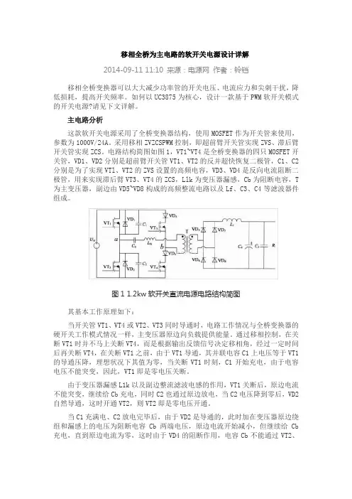
主电路分析这款软开关电源采用了全桥变换器结构,使用MOSFET作为开关管来使用,参数为1000V/24A。
采用移相ZVZCSPWM控制,即超前臂开关管实现ZVS、滞后臂开关管实现ZCS。
电路结构简图如图1,VT1~VT4是全桥变换器的四只MOSFET开关管,VD1、VD2分别是超前臂开关管VT1、VT2的反并超快恢复二极管,C1、C2分别是为了实现VTl、VT2的ZVS设置的高频电容,VD3、VD4是反向电流阻断二极管,用来实现滞后臂VT3、VT4的ZCS,Llk为变压器漏感,Cb为阻断电容,T 为主变压器,副边由VD5~VD8构成的高频整流电路以及Lf、C3、C4等滤波器件组成。
图1 1.2kw软开关直流电源电路结构简图其基本工作原理如下:当开关管VT1、VT4或VT2、VT3同时导通时,电路工作情况与全桥变换器的硬开关工作模式情况一样,主变压器原边向负载提供能量。
通过移相控制,在关断VT1时并不马上关断VT4,而是根据输出反馈信号决定移相角,经过一定时间后再关断VT4,在关断VT1之前,由于VT1导通,其并联电容C1上电压等于VT1的导通压降,理想状况下其值为零,当关断VT1时刻,C1开始充电,由于电容电压不能突变,因此,VT1即是零电压关断。
由于变压器漏感L1k以及副边整流滤波电感的作用,VT1关断后,原边电流不能突变,继续给Cb充电,同时C2也通过原边放电,当C2电压降到零后,VD2自然导通,这时开通VT2,则VT2即是零电压开通。
当C1充满电、C2放电完毕后,由于VD2是导通的,此时加在变压器原边绕组和漏感上的电压为阻断电容Cb两端电压,原边电流开始减小,但继续给Cb 充电,直到原边电流为零,这时由于VD4的阻断作用,电容Cb不能通过VT2、VT4、VD4进行放电,Cb两端电压维持不变,这时流过VT4电流为零,关断VT4即是零电流关断。
引言随着计算机与通信技术的飞速发展,作为配套设备的开关电源也获得了长足进步,并随着新器件、新理论、新电磁材料和变换技术以及各种辅助设计分析软件的不断问世,开关电源的性能不断提高。
本文介绍一种新型的高频DC/DC开关变换器,并成功地应用在军用充电机上。
DC/DC变换器主电路改进型移相全桥ZVS DC/DC变换器主电路结构和各点波形对照如图1、图2所示。
由于电路工作状态在一个周期内可以分为两个完全一样的过程,所以以下仅仅分析半个周期的情况,而这半个周期又可分为以下三种开关模态。
● 开关模态1,t0<t<t1,其中t1=DT s/2此时Q1和Q4同时导通,变压器副边电感L1和整流管D S2导通,原边能量向负载端传递。
此模态的等效电路见图3。
其中,a为变压器变比,V in是直流母线电压,I1和I2分别是电感L1和L2电流(L1=L2=LS),此时有等式(1)成立。
(1)(2)I p(t)=aI1(t)(3)当Q4关断时该模态过程结束。
● 开关模态2,t1<t<t2,其中t2≤T s/2在t1时刻关断Q4,此时副边电感L1中储存的能量给Q4电容(或并联电容)充电,同时将Q3两端电容电荷放掉。
为了实现软开关,Q4关断和Q3开通之间至少要存在一死区时间Δt1,使得在Q3开通前D3首先导通,且有下式成立。
I p1Δt1=2C eff V in(4)其中C eff是开关管漏源两端等效电容,I P1为t1时刻变压器原边流过电流。
当D3导通后,变压器副边两个二极管D S1和D S2同时导通,电路工作在续流状态。
此时等效电路如图4所示。
此时有如下电路方程成立。
(5)(6)(7)(8)r t=r mosfet+r xfmr (9)其中D为脉冲占空比,f S为电路工作频率,L’ik为主边变压器漏感(或与外接电感的串联值),rt是变压器原边等效电阻,τ是原边等效电流衰减时间常数,Vfp是反并联二极管导通压降。

移相谐振全桥软开关控制器UCC38951、引言UCC3895是美国德州仪器公司生产的移相谐振全桥软开关控制器,该系列控制器采用了先进的BCDMOS技术。
UCC3895在基本功能上与UC3875系列和UC3879系列控制器完全相同,同时增加了一些新的功能。
下面对其特点、引脚功能、电气参数、工作原理分别进行介绍。
2、特点和引脚说明2.1 特点(1)输出导通延迟时间编程可控;(2)自适应延迟时间设置功能;(3)双向振荡器同步功能;(4)电压模式控制或电流模式控制;(5)软启动/软关机和控制器片选功能编程可控,单引脚控制;(6)占空比控制范围0%~100%;(7)内置7MHz误差放大器;(8)最高工作频率达到1MHz;(9)工作电流低,500KHz下的工作电流仅为5mA;(10)欠压锁定状态下的电流仅为150μA。
2.2 引脚说明UCC3895和UCC2895移相谐振全桥软开关控制器采用SOIC-20、PDIP-20、TSSOP-20和PLCC-20四种封装形式,UCC1895采用CDIP-20和CLCC-20两种封装形式。
下面以PDIP-20为例进行介绍,其引脚排列如图1所示。
UCC3895系列移相谐振控制器采的引脚功能简介如下:•EAN(引脚1):误差放大器反相输入端。
•EAOUT(引脚2):误差放大器输出端。
在控制器内部,该端分别与PWM比较器和空载比较器的非反相输入端相连,并箝位于软启动电压。
当该端上的电压低于500mV时,控制器的输出级将被空载比较器关断。
当该端上的电压升至600mV时,输出级重新开通。
•RAMP(引脚3):PWM比较器的非反相输入端。
在电压模式或平均电流模式下,该端接CT(引脚7)上的锯齿波信号;而在峰值电流模式下,该端接电流信号。
RAMP内接放电晶体管,该晶体管在振荡器死区时间内触发。
•REF(引脚4):精密5V基准电压输出端。
控制器内部的基准电源一方面为控制器内部的电路供电,另一方面还能够向外接负载提供5mA的偏置电流。
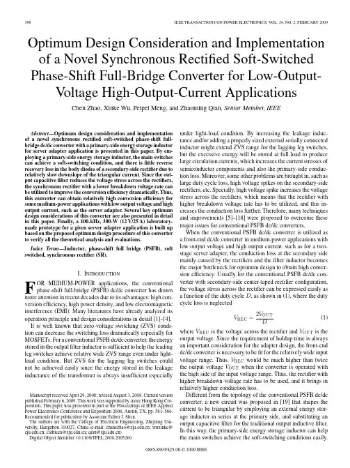
Optimum Design Consideration and Implementation of a Novel Synchronous Rectified Soft-Switched Phase-Shift Full-Bridge Converter for Low-Output-V oltage High-Output-Current Applications Chen Zhao,Xinke Wu,Peipei Meng,and Zhaoming Qian,Senior Member,IEEEAbstract—Optimum design consideration and implementation of a novel synchronous rectified soft-switched phase-shift full-bridge dc/dc converter with a primary-side energy storage inductor for server adapter application is presented in this paper.By em-ploying a primary-side energy storage inductor,the main switches can achieve a soft-switching condition,and there is little reverse recovery loss in the body diodes of a secondary-side rectifier due to relatively slow downslope of the triangular current.Since the out-put capacitivefilter reduces the voltage stress across the rectifiers, the synchronous rectifier with a lower breakdown voltage rate can be utilized to improve the conversion efficiency dramatically.Thus, this converter can obtain relatively high conversion efficiency for some medium-power applications with low output voltage and high output current,such as the server adapter.Several key optimum design considerations of this converter are also presented in detail in this paper.Finally,a100-kHz,300-W(12V/25A)laboratory-made prototype for a given server adapter application is built up based on the proposed optimum design procedure of this converter to verify all the theoretical analysis and evaluations.Index Terms—Inductor,phase-shift full bridge(PSFB),soft switched,synchronous rectifier(SR).I.I NTRODUCTIONF OR MEDIUM-POWER applications,the conventionalphase-shift full-bridge(PSFB)dc/dc converter has drawn more attention in recent decades due to its advantages:high con-version efficiency,high power density,and low electromagnetic interference(EMI).Many literatures have already analyzed its operation principle and design considerations in detail[1]–[4]. It is well known that zero-voltage switching(ZVS)condi-tion can decrease the switching loss dramatically especially for MOSFETs.For a conventional PSFB dc/dc converter,the energy stored in the outputfilter inductor is sufficient to help the leading leg switches achieve relative wide ZVS range even under light-load condition.But ZVS for the lagging leg switches could not be achieved easily since the energy stored in the leakage inductance of the transformer is always insufficient especiallyManuscript received April29,2008;revised August3,2008.Current version published February6,2009.This work was supported by Astec Hong Kong Cor-poration.This paper was presented in part at the Proceedings of IEEE Applied Power Electronics Conference and Exposition2008,Austin,TX,pp.581–586. Recommended for publication by Associate Editor J.Shen.The authors are with the College of Electrical Engineering,Zhejiang Uni-versity,Hangzhou310027,China(e-mail:chanezhao@;wuxinke@ ;cathleen@;qian@).Digital Object Identifier10.1109/TPEL.2008.2005269under light-load condition.By increasing the leakage induc-tance and/or adding a properly sized external serially connected inductor might extend ZVS range for the lagging leg switches, but the excessive energy will be stored at full load to produce large circulation currents,which increases the current stresses of semiconductor components and also the primary-side conduc-tion loss.Moreover,some other problems are brought in,such as large duty cycle loss,high voltage spikes on the secondary-side rectifiers,etc.Specially,high voltage spike increases the voltage stress across the rectifiers,which means that the rectifier with higher breakdown voltage rate has to be utilized,and this in-creases the conduction loss further.Therefore,many techniques and improvements[5]–[18]were proposed to overcome these major issues for conventional PSFB dc/dc converters.When the conventional PSFB dc/dc converter is utilized as a front-end dc/dc converter in medium-power applications with low output voltage and high output current,such as for a two-stage server adapter,the conduction loss at the secondary side mainly caused by the rectifiers and thefilter inductor becomes the major bottleneck for optimum design to obtain high conver-sion effiually for the conventional PSFB dc/dc con-verter with secondary-side center-taped rectifier configuration, the voltage stress across the rectifier can be expressed easily as a function of the duty cycle D,as shown in(1),where the duty cycle loss is neglectedV REC=2V OUTD(1) where V REC is the voltage across the rectifier and V OUT is the output voltage.Since the requirement of holdup time is always an important consideration for the adapter design,the front-end dc/dc converter is necessary to befit for the relatively wide input voltage range.Thus,V REC would be much higher than twice the output voltage V OUT when the converter is operated with the high side of the input voltage range.Thus,the rectifier with higher breakdown voltage rate has to be used,and it brings in relatively higher conduction loss.Different from the topology of the conventional PSFB dc/dc converter,a new circuit was proposed in[19]that shapes the current to be triangular by employing an external energy stor-age inductor in series at the primary side,and substituting an output capacitivefilter for the traditional output inductivefilter. In this way,the primary-side energy storage inductor can help the main switches achieve the soft-switching conditions easily.0885-8993/$25.00©2009IEEEThe reverse recovery loss in the diode rectifiers or the body diodes of the synchronous rectifier(SR)can be reduced a lot due to the relatively slow downslope of the triangular current.The voltage stress across the rectifiers can be reduced and clamped by the output voltage directly.Thus,the rectifier with a lower breakdown voltage rate can be used to reduce the secondary-side conduction loss.Unfortunately,sufficient design considerations for the engineers are provided in[19].Following the same idea presented in[19],another topology proposed in[20]employs the PS strategy to control the primary-side switches and the secondary-side switches.It can be designed to operate in step-down mode and step-up mode,respectively.The MOSFETs can achieve ZVS condition easily,and the diode rectifiers can turn off in zero-current switching(ZCS)condition.However,the control circuit is rather complex due to the additional isolating control design for the secondary-side switches.Besides,when in the step-down operation mode,this converter cannot be op-erated with null-load.It would be fatal problem if the front-end dc/dc converter is designed for the adapter applications.The en-ergy storage inductor is set before the rectifiers at the secondary side in[21]and[22].They have similar operation principles and characteristics as in[19]for high-power applications with high output voltage and low output current,but not suitable for medium-power server adapter applications.In order to obtain high conversion efficiency for medium-power applications with low output voltage and high output current,a new synchronous rectified soft-switched PSFB dc/dc converter with a primary-side energy storage inductor based on[19]–[22]is studied and implemented in this paper.Many current-mode-driven strategies for the SR are already proposed [25]–[28],whereas the strategy proposed in[27]and[28]is utilized to drive the SR in this converter.Section II presents the principle analysis of the selected appropriate operation modes when this converter is designed as a front-end dc/dc converter for medium-power server adapter applications.Section III fo-cuses on several key optimum design considerations of this converter.Successively,an optimum design procedure of this converter is proposed,and is supposed to be the design refer-ence for other engineers.Finally,a100-kHz,300-W(12V/25A) laboratory-made prototype is built up to verify all the theoret-ical analysis and evaluation.The highest full-load conversion efficiency of this converter reaches about95.9%.Compared with the traditional PSFB dc/dc converter,its advantage in high conversion efficiency shows good potential for medium-power server adapter applications.II.P RINCIPLE OF THE S ELECTEDA PPROPRIATE O PERATION M ODEFig.1shows the basic topology of this converter,where Q1–Q4are the primary-side main switches paralleled with D C1P–D C4as their body diodes.C OSS1–C OSS4are their par-asitic paralleled capacitances.L R is the added external energy storage inductor in series at the primary side.C B is the series dc block capacitor.T is a traditional center-taped transformer. To reduce the secondary-side conduction loss,the synchronous rectifiers SR1and SR2are utilized and paralleled with D SR1and Fig.1.Topology of the presented synchronous rectified PSFB converter with primary-side energy storage inductor[23],[28].D SR2as their body diodes.C SR1and C SR2are their parasiticparalleled capacitances.The SRs are driven by the strategy pro-posed in[27]and[28].CT1and CT2are the current detectors.C O is the outputfilter capacitor.R LOAD is the output load.This converter can be designed to operate in three differentmodes,which are defined according to the operation of theprimary-side currentflow I PRI.When there is an idle intervalof I PRI in one switching period,this operation mode is definedas the discontinuous conduction mode(DCM);if I PRI reacheszero exactly at the time when the lagging leg switches are turned OFF,this operation mode is defined as the boundary conduction mode(BCM);if I PRI does not reach zero at the time whenthe lagging leg switches are turned OFF,this operation mode isdefined as the continuous conduction mode(CCM).Therefore,thefirst and the most important step of the whole design processis to select the appropriate operation modes that arefit for themedium-power applications.A.Appropriate Operation Modes SelectionWhen the converter is designed to be operated in DCM mode,the primary-side energy storage inductor L R can easily help theleading leg switches achieve wide range ZVS and help the lag-ging leg switches achieve entire range ZCS without any otherauxiliary circuit.The detailed soft-switching analysis is pre-sented in Section III.There is little reverse recovery loss in theSRs’body diodes at the secondary side due to the relativelyslow downslope of the triangular current.Additionally,the volt-age stress across the rectifiers can be restrained by the outputvoltage clamping,which means that the feasibility of utilizingthe SRs with lower breakdown voltage rate will improve theconversion efficiency.The energy stored in the primary-sideleakage inductance of the transformer is accommodated by L R;thus,there is no more duty cycle loss and circulation loss.How-ever,with the same input voltage,output power,and the turnratio of transformer,the converter would have a relatively largerrms current in DCM mode than that in CCM mode or BCMmode.When operated in BCM mode,it not only preserves all advan-tages as when operated in DCM,but also with relatively lesserrms current,which means that the conduction loss is reduced.Unfortunately,controlled by the PS strategy,the BCM operationmode can be maintained only under a given operation conditionof this buck-derived converter.When operated in CCM mode,although the converter hasrelatively smallest rms current and ZVS conditions can simplybe achieved for both the leading leg switches and the lagging legswitches,the extremely narrow range of dc gain variation resultsin the extremely wide range of duty cycle variation in order tomeet the requirement of the input voltage range.It increases thedifficulty in optimum design for the transformer and definitelythe energy storage inductor.This issue will also be analyzed inSection III.Moreover,operation in CCM mode also leads to therelatively faster downslope of the current,which would causethe high voltage spikes on SRs and the large reverse recoveryloss in SRs’body diodes.Based on the aforementioned discussion,for medium-powerapplications with low output voltage and high output current,DCM mode is always suitable for this presented converter.Spe-cially,BCM mode can be designed for this converter under thefollowing operation conditions:low side of the input voltagerange and full-load output power.The detailed operation princi-ple of CCM mode can be obtained in a previous work[23]andare not presented in this paper.B.Principle Analysis of the Selected AppropriateOperation ModeTo be brief,this part mainly focuses on the operation prin-ciple of this converter when operated in DCM mode,and theBCM mode can simply be considered as the critical case of theDCM mode.Some reasonable assumptions are listed primarilyto simplify the operation analysis process:1)all the magneticcomponents are ideal:the magnetizing inductance of the trans-former is so large that the magnetizing current can be neglected.The leakage inductances of the transformer no matter at the pri-mary side or at the secondary side are both omitted;2)all thecapacitors are constant and linear;and3)the forward voltage ofdiodes and the R DSON of MOSFETs are not considered.Fig.2shows the theoretical waveforms and the equivalent circuits offive operation modes during a half switching period when thisconverter is operated in DCM mode.1)Mode1(t0–t1):During this active state,the primary-side main switches Q1and Q3are ON,the secondary-side syn-chronous rectifier SR2turns on at t0with the current-drivenstrategy[28],and the power is transferred from input side to out-put side.V AB equals the input voltage V IN.The voltage acrossthe transformer’s primary-side winding V Trans is clamped bythe output voltage at nV OUT.The voltage across SR1,V SR1,is also clamped by the output voltage at2V o.L R takes thepositive voltage stress(V IN−nV o).The secondary-side current increases with positive slope as shown in(2),which is n timesthe primary-side current.This mode ends at t1when Q1turnsoffdi SEC dt =ndi PRIdt=nV LRL R=nV IN−nV OUTL R(2)where n is the turns ratio of the transformer.2)Mode2(t1–t2):When the primary-side main switch Q1 turns off at t1,then the parasitic paralleled capacitances C OSS1 and C OSS2of the leading leg switches Q1and Q2are charged and discharged by the primary-side current,respectively.To simplify the analysis,the primary-side current i PRI can be con-sidered as a constant current source I PRI during this short inter-val because the energy stored in L R is large enough.Sincethe Fig.2.Theoretical waveforms and the equivalent circuits offive operation modes in DCM.primary-side leading leg switches are always of the same type, the parasitic paralleled capacitances C OSS1and C OSS2can also be supposed to be equal to a constant capacitance C OSS.Thus, the voltages stress across C OSS1and C OSS2can be expressed in(3)and(4),respectively.When the voltage across C OSS2 reaches zero,the body diode of main switches Q2,D C2,turns on for the primary-side circulation.Then,switch Q2can turn on with ZVS.Obviously,the dead time T DEAD between the driven signals of Q1and Q2should exactly befit for(5).This interval ends at t2when Q2turns onV CO S S1(t)=(V IN−nV OUT)(t1−t0)2L R C OSS(t−t1)(3)V CO S S2(t)=V IN−(V IN−nV OUT)(t1−t0)2L R C OSS(t−t1)(4) T DEAD≥2V IN L R C OSS(V IN−nV OUT)(t1−t0).(5)3)Mode3(t2−t3):When the main switch Q2turns on with ZVS at t2,V AB equals to zero.Since the primary-side current maintains itsflow direction,V Trans keeps its polarity and is still clamped at nV OUT,and SR2conducts continuously.Thus, L R takes the negative voltage stress(−nV OUT)to achieve the volt·seconds balance.The primary-side current i PRI expressed in(6)decreases with the negative slope(−nV OUT/L R).The secondary-side current i SEC also decreases with the negative slope,but n times the primary-side current.This mode ends at t3when the primary-side current i PRI reaches zeroi PRI(t)=(V IN−nV OUT)(t1−t0)L R−nV OUTL R(t−t2).(6)TABLE IB ASIC S PECIFICATIONS OF A T YPICAL M EDIUM -P OWER S ERVERA DAPTER APPLICATION4)Mode 4(t 3−t 4):At t 3,both the primary-side and the secondary-side currents fall to zero.Thus,the lagging leg switch Q 3as well as the synchronous rectifier SR 2can turn off with ZCS.However,for the MOSFETs,ZVS condition can be more beneficial than ZCS condition.Section III will analyze the ZVS condition of the primary-side switches in detail.During this interval,both V Trans and V LR are at 0V .The voltage stress across the SRs is clamped at V OUT if the parasitical resonance between the leakage inductance and parasitical capacitance is neglected.This interval ends at t 4when the lagging leg switch Q 3turns off with ZCS.5)Mode 5(t 4−t 5):Since the parasitic capacitance and leak-age inductance are neglected and the magnetizing inductance of transformer is large enough,before the lagging leg switch Q 4turning on,there would be no voltage balance current flow,nei-ther in C OSS3nor in C OSS4even if the lagging leg switch Q 3is already turned off.When the lagging leg switch Q 4turns on at t 5,the charging current of C OSS3and the discharging current of C OSS4flow through it together,and the obvious current spike results in the turn-on switching loss in the lagging leg switches.After mode 5,this converter begins to operate in another half switching pared with the DCM,the BCM does not have the idle interval mode 4,as shown in the shadow area of the theoretical waveforms.III.S EVERAL K EY O PTIMUM D ESIGN C ONSIDERATIONS To obtain relatively higher conversion efficiency for the medium-power applications especially as the server adapter,some key optimum design considerations are necessary to be taken into account for this converter.First,the steady-state analysis is proposed,which can help the engineers realize the dc gain variable range of this converter in different operation modes.Second,the maximum duty cycle and the parameters of the magnetic components,which affect the conversion efficiency directly,should be designed carefully.Then,the ZVS range analysis of the primary-side main switches shows the capability in the reduction of switching loss.More-over,the analysis of the voltage stress across the secondary-side SRs,when considering the impact of the secondary-side leakage inductances of the transformer,is necessary for the selection of the breakdown voltage rate for SRs.The current stress in the output capacitive filter is also presented.Table I shows the basic specifications of a typical medium-power server adapter appli-cation with low output voltage and high output current.A.Steady-State Analysis of This ConverterAs mentioned earlier,this converter can be designed to oper-ate in three different modes:DCM,BCM,or CCM.To simplify the steady-state analysis,the dead time between the drivensig-Fig.3.(a)DC gain characteristic of this converter.n =24;L R =120µH;V IN =350V .(b)Relationship between the duty cycle and the output load.n =24;L R =120µH.nals of one-bridge leg switches is omitted in this part.When operated in DCM mode,the dc gain characteristic of this con-verter can be derived from the volt ·seconds balance on L R and the basic principle of energy conservation.It is equivalent to the buck-derived converter operated in DCM mode.Based on (7)and (8),it is easy to obtain the dc gain characteristic in DCM of this converter as shown in (9)V IN −nV OUTL R (t 2−t 0)=nV OUT L R (t 3−t 2)(7)2(V IN −nV OUT )(t 2−t 0)(t 3−t 0)T S L R =V OUTnR LOAD (8)Gain DCM=V OUT V IN =nD 2T S R LOAD 8L R × 1+16L RD T S R LOAD n −1(9)where T S is the switching period and D is the duty cycle defined as D =2(t 2−t 0)/T S .When operated in BCM mode,the dc gain characteristic can be derived directly via the volt ·seconds balance on L R asGain BCM =V OUT V IN =Dn.(10)When operated in CCM mode,the theoretical waveformscan be seen from [23].Then,the dc gain characteristic can be derived in the same way as well as operated in DCM.Based on the integral equation (11),the dc gain of CCM is obtained as shown in (12)2 T S /20i PRI dt T S =V OUTnR LOAD(11)Gain CCM =V OUT V IN =16L 2Rn 6T 2S R 2LOAD−D 2n 2+2D n 2−4L Rn 3T S R LOAD.(12)Fig.3(a)shows the dc gain characteristic of this converter with the given parameters.It can be seen that the curve slope in CCMrange is extremely slow,which indicates the extremely narrow variable range of the dc gain.The extremely narrow variable dc gain range always needs wide duty cycle variable range and small turn ratio of the transformer to meet the requirement of the input voltage range.Thus,operation in CCM mode would bring in more difficulty in the optimum design for the magnetic components(both the added energy storage inductor L R and the transformer)and more conduction loss at the primary side. Moreover,the relatively fast downslope of the current in CCM mode also causes the voltage spikes and increases the voltage stress across the secondary-side SRs.Therefore,this converter is not suitable to operate in CCM mode especially for the medium-power server adapter applications.Furthermore,for the buck-derived converter controlled by the PS strategy,the BCM mode has only one point on the dc gain curve.Considering the advantages that BCM have,it is optimum to make this converter operate in BCM mode exactly with the low side of the input voltage,V IN LOW,and the full-load output power,as mentioned in Section II.Fig.3(b)shows the relationship between the duty cycle D and the output load R LOAD.B.Optimum Design for the Maximum Duty Cycle and the Magnetic ComponentsBased on the aforementioned steady-state analysis,this con-verter prefers to operate in BCM with350-V input voltage and full-load output power.This case requires the maximum duty cycle operation,which means that D BCM should be equal to D MAX.Hence,the optimum design for D MAX would be nec-essary for obtaining the high conversion efficiency in BCM operation.The rms value of the triangular current in BCM at the primary side can be expressed as a function of D MAX in(13). But the current at the secondary side is determined only by the output power,as shown in(14).Thus,D MAX would obviously affect the primary-side conduction lossI rms P(D MAX)=2√3I OUT V OUT3D MAX V IN(13)I rms S=2√3P OUT3V OUT.(14)Generally,(10)can determine the turn ratio of the transformer directly.For the server adapter applications,the secondary-side winding turns are usually as small as possible in order to reduce the conduction loss effectively.But it results in larger core loss of the transformer due to the fewer turns of the primary-side winding.Equation(15)shows the acflux density of the trans-former as a function of D MAX.Thus,the conduction loss and the core loss of the transformer can also be a function of D MAX, and the tradeoff between them should be taken into account carefully∆B T(D MAX)=D MAX T S V IN4N P A CT(15)where N P is the turns of the primary-side winding of the trans-former and A CT is the effective cross-sectional area of trans-former core’s magneticcircuit.Fig.4.Loss tradeoff results of the optimum design for the D B C M and the magnetic components.For the series energy storage inductor L R,it is necessary to tradeoff the conduction loss and core loss as well as the transformer.Equations(16)and(17)show the inductance and the winding turns of L R as a function of D MAX separately L R(D MAX)=D2MAX T S R OUT(1−D MAX)4G2BCM(16)N LR(D MAX)=V IN T S D MAX(1−D MAX)4∆B LRA CLR(17)where∆B LRis the acflux density of L R and A CLR is the effective cross-sectional area of L R core’s magnetic circuit. Although∆B LRis an unknown quantity as well as the wind-ing turns of L R,it can usually be given before one cycle of the design procedure to simplify the optimum design process. Then,the relatively optimum value of∆B LRcan be obtained through several cycles of the design procedure.Thus,during one cycle of the design procedure with the given value of∆B LR, the tradeoff between conduction loss and core loss of L R can also be derived by the equations of D MAX.Therefore,the optimum design for D MAX can be obtained based on the loss tradeoff among three main parts,such as the primary-side conduction loss in semiconductor components,the transformer loss,and the added series energy storage inductor loss.Fig.4shows the tradeoff results of four different design cases separately.All of them have the same tendency,i.e.,the loss clearly decreases with increase of D BCM.However,larger D BCM results in the faster downslope of the triangular current in BCM mode,which would increase the reverse recovery loss in SRs’body diodes and the design difficulty and complexity in turn-off control circuit of SRs.Luckily,it can also be seen that when D MAX is larger than0.6approximately,little benefit in loss reduction can be gained by increasing D MAX.It means that the duty cycle range shown in the shadow area should be the relatively optimum range of D MAX.Then,the optimum design for the transformer and L R can be derived by the comparison of several tradeoff result curves,which can be done easily by the program in the computer.Fig.5.ZVS range of the leading leg switches.(a)n =24;C O S S =120pF;T D E A D =200ns;V O U T =12V;V IN =350V .(b)L R =120µH;n =24;C O S S =120pF;T D E A D =200ns;V O U T =12V.Fig.6.Theoretic waveforms of the primary-side current i P R I and the mag-netizing current i M .C.Soft-Switching Analysis for the Primary-Side Main Switches As mentioned earlier,the primary-side series energy storage inductor L R and the output capacitive filter are employed for this converter to have a triangular shape of the current flow.Thus,for the primary-side leading leg switches,the wide load-range zero-voltage turn-on can be achieved easily by the sufficient energy stored in L R without any other auxiliary circuit.To simplify the analysis process,ZVS range of the leading leg switches can be defined as (18).When (18)is greater than unity,the leading leg switches can achieve ZVS;when (18)is lesser than unity,ZVS will be lost.Fig.5shows ZVS range of the leading leg switches,where Fig.5(a)shows the relationship between ZVS range and two variable factors,the inductance of L R and the output load R LOAD .As R LOAD becomes lighter,L R needs to decrease to maintain ZVS for the leading leg switches.Fig.5(b)indicates that with the relatively optimum design for L R ,the leading leg switches can achieve ZVS approximately from 5%load to full-load.Sometimes,the transformer’s magnetic cur-rent is designed to help the primary-side lagging leg switches achieve ZVS.Fig.6shows the theoretic waveforms of i PRI and the transformer magnetizing current i M ,when this converter is operated in DCM mode.It can be seen that if ∆T 1is lesser than ∆T 2,the magnetizing current i M would help further widen ZVS range for the leading leg switches.On the contrary,when ∆T 1is larger than ∆T 2,the magnetizing current i M would deterio-rate ZVS range of the leading leg switches.Thus,(20)should be valid to guarantee ZVS range for the leading leg switches,which means that the input voltage range should also be a designconsideration for ZVS range of the leading leg switchesZVS LEAD (R LOAD )=T DEAD T C O S S(18)where T C O S S is the charge or discharge time of the parasitic paralleled capacitances of the leading leg switches,and can be expressed asT C O S S (R LOAD )=2C OSS V OUT /V IN1−n V O U T VI NT S /(R LOAD L R )(19)V IN HIGH V INLOW≤2D MAX=2D BCM.(20)If the magnetizing current of the transformer is small enough,the lagging leg switches can definitely achieve the entire range zero-current turn-off when this converter is operated in BCM mode or DCM mode.But MOSFETs always obtain more bene-fit in the reduction of switching loss from zero-voltage turn-on than that from zero-current turn-off.The current spike at the hard-switching turn-on mentioned in Section II would cause the considerable switching loss in the lagging leg switches.ZVS for the lagging leg switches can be achieved by several ways.First one is to increase the magnetizing current of the trans-former without any other auxiliary circuit.However,sufficient magnetizing current also increases the conduction loss both in the primary-side semiconductor components and the mag-netic components.ZVS condition is load-dependent as well.The second way is to utilize a simple LC auxiliary resonant circuit proposed in [12]–[14].It can easily achieve the load-independent ZVS for the lagging leg switches and increases the additional conduction loss only in the lagging leg switches and the auxiliary circuit,which is less than that of the first way.Fig.10(a)shows the presented converter with this auxiliary res-onant circuit,and the auxiliary inductance L AUX should be fit for (21)to ensure the load-independent ZVS for the lagging leg switches.The third way is to employ the other LC auxiliary resonant circuit proposed in [15].It can self-adaptively achieve ZVS for all the main switches over the entire conversion range with small conduction loss penalty.But the design and imple-mentation of it are little more difficult than that of the second approach.L AUX ≤T DEAD T S16C OSS.(21)D.Voltage Stress Across the Secondary-Side SRsTheoretically,the voltage stress across the secondary-side SRs should be clamped at twice of the output voltage (2V OUT )exactly.However,when the impact of the secondary-side leak-age inductances of the transformer is taken into account,the practical voltage stress across the SRs would be higher than 2V OUT .For the traditional center-taped rectifier configuration with inductive output filter,there is always little current ripple flow-ing though the secondary-side leakage inductances L KS of the。

基于移相全桥软开关技术的应用引言随着科技的发展,电力电子设备不断更新,电源称为了现代工业、国防和科学研究中不可缺少的电气设备。
为了触发、驱动开关变换器的功率开关管,研制适应越来越高性能要求的开关电源,近年来出现了PWM(脉宽调制)型变换器。
PWM技术应用广泛,构成的变换器结构简单,它对常用的线性调节电源提出挑战,在减小体积的同时获取更大的功率密度和更高的系统效率[1,2]。
为了拓展开关电源的应用场合,电源工作频率逐渐提高,高频化成为其重要发展方向,同时也是减小开关电源尺寸的最有效手段。
然而高频PWM变换器在传统硬开关方式工作下,功率管损耗较为严重,系统效率不高,随着开关频率的逐步提高,损耗相继增大[3,4]。
为此,必须采取措施以提高高频开关变换器的效率,人们研究了软开关技术,除了减小开关损耗外,软开关技术应用还大大降低了开关噪声、减小了电磁干扰。
软开关技术概况及发展目前广泛应用的DC-DC PWM功率变换技术是一种硬开关技术。
所谓“硬开关”是指功率开关管的开通或者关断是在器件上的电压或者电流不等于零的状态下进行的,即强迫器件在其电压不为零时开通,或电流不为零时关断。
调高开关频率是开关变换技术的重要的发展方向之一。
其原因是高频化可以使开关变换器的体积、重量大为减小,从而提高变换器的功率密度。
为了使开关电源能够在高频下高效率的运行,高频软开关技术不断的发展,所谓“软开关”指的零电压开关(Zero Voltage Switching, ZVS)或零电流开关(Zero Current Switching, ZCS)[5]。
它是应用谐振原理,使开关变换器的开关器件中电流(或电压)按正弦或准正弦规律变化,当电流自然过零时,使器件关断;或者电压为零时,使器件开通,实现开关损耗为零。
再加入一些说明移相全桥DC-DC技术传统的全桥(full-bridge简称FB)PWM变换器适用于输出低电压、大功率的情况,以及电源电压和负载变流变换大的场合。
ZVZCS移相全桥软开关工作原理(1) 主电路拓扑本设计采用ZVZCS PWM移相全桥变换器,采用增加辅助电路得方法复位变压器原边电流,实现了超前桥臂得零电压开关(ZVS)与滞后桥臂得零电流开关(ZCS)。
电路拓扑如图3、6所示。
图3、6 全桥ZVZCS电路拓扑当、导通时,电源对变压器初级绕组正向充电,将能量提供给负载,同时,输出端钳位电容充电。
当关断时,电源对充电,通过变压器初级绕组放电。
由于得存在,为零电压关断,此时变压器漏感与输出滤波电感串联,共同提供能量,由于得存在使得变压器副边电压下降速度比原边慢,导致电位差并产生感应电动势作用于,加速了得放电,为得零电压开通提供条件。
当放电完全后,整流二极管全部导通续流,在续流期间原边电流已复位,此时关段,开通,由于漏感两边电流不能突变,所以为零电流关断,为零电流开通。
(2)主电路工作过程分析[7]半个周期内将全桥变换器得工作状态分为8种模式。
①模式1、导通,电源对变压器初级绕组正向充电,将能量提供给负载,同时,输出端箝位电容充电。
输出滤波电感与漏感相比较大,视为恒流源,主电路简化图及等效电路图如图3、7所示。
图3、7模式1主电路简化图及等效电路图由上图可以得到如下方程:(3-3)(3-4)(3-5)由(3-3)式得:(3-6)将(3-6)式代入(3-5)式得:(3-7)将(3-7)式代入(3-4)式得:(3-8)解微分方程:(3-9)其初始条件为:; (3-10)代入方程解得:(3-11)(3-12)(3-13)(其中)②模式2当时,达到最大值,此时,,;二极管关断,输出侧电流流经、、、、与次级绕组,简化电路如图3、8所示。
此时满足:,,。
图3、8模式2简化电路图③模式3S1关断,原边电流从S1转移至C1与C2,C1充电,C2放电,简化电路如图3、9所示。
由于C1得存在,S1就是零电压关断。
变压器原边漏感与输出滤波电感串联,共同提供能量,变压器原边电压与整流桥输出电压以相同得斜率线性下降,满足:。
2005年12月重庆大学学报(自然科学版)D ec.2005第28卷第12期Jour nal of Chongqi n g U niversity(Nõt u rõl Sc ience Ed ition)V o.l28No.12文章编号:1000-582X(2005)12-0027-05移相全桥软开关变换器拓扑分析*陈柬,陆治国(重庆大学电气工程学院,重庆400030)摘要:移相全桥软开关变换器从基本的移相全桥(FB)零电压(Z VS)脉宽调制(P WM)变换器,发展到移相全桥零电压零电流(ZVZCS)P WM变换器,及移相全桥零电流(ZCS)P WM变换器,进而又产生一系列其它新型的移相全桥电路,构成了这一类很具有发展和应用前景的变换器.比较分析了上述3类主要的移相全桥软开关变换器的拓扑结构、工作特点和各自的优缺点.改进的FB-Z VS-P WM变换器扩大了滞后臂Z VS负载范围.FB-ZVZCS-P WM变换器解决了滞后臂软开关负载范围问题,滞后臂较适合用绝缘栅极双极型晶体管(I G B T).FB-ZCS-P WM变换器可以实现各个功率管的ZCS,更适合大功率场合.关键词:移相;零电压开关;零电流开关;零电压零电流开关;变换器中图分类号:TM910.1文献标识码:A移相P WM控制方式是近年来在全桥变换电路中广泛应用的一种软开关控制方式.这种控制方式实际上是谐振变换技术与常规P WM变换技术的结合.移相全桥软开关电路有效降低了电路的开关损耗和开关噪声,减少了器件开关过程中产生的电磁干扰,为变换器装置提高开关频率和效率降低尺寸及重量提供了良好的条件.同时,还保持了常规的全桥P WM电路中拓扑结构简洁,控制方式简单,开关频率恒定,元器件的电压和电流应力小等一系列优点.1移相FB-Z VS-P WM变换器1.1基本的移相FB-ZVS-P WM变换器移相全桥零电压P WM软开关的实际电路如图1所示[1-3].图1基本的移相FB-ZVS-P WM变换器图2是Q1~Q4的开关控制波形.与常规的全桥P WM相比,移相式FB-Z VS-P WM变换器具有明显的优势.利用变压器漏感和开关管的结电容谐振,在不增加额外元器件的情况下,通过移相控制方式,实现了功率开关管的零电压导通与关断,减小了开关损耗,降低了开关噪声,提高了效率,减小整机的体积与重量.其主要缺点为:滞后臂开关管在轻载下将失去零电压开关功能;原边有较大环流,增加了系统的通态损耗;存在占空比丢失现象[3-8].图2开关控制波形1.2串联饱和电感的改进拓扑在变压器初级串联饱和电感L r的方案中[9],利用L r的临界饱和电流特性及储能,来扩大Z VS的负载范围,提高轻载时的输出效率.与图1所示变换器相比,它具有明显的优势:有效扩大了零电压开关负载范围,*收稿日期:2005-08-10作者简介:陈柬(1981-),女,河南南阳人,重庆大学硕士,主要从事电力电子与电力传动方向的研究.保持了最小的环流能量,减小了导通损耗;减小占空比丢失;改善了输出电压调节特性;减小了副边整流二极管结电容的寄生振荡.1.3输出滤波电感参与谐振的改进拓扑这种电路在滞后臂开关管进行状态转换的短暂期间,使副边整流二极管不能同时导通,则输出滤波电感可被用来参与谐振.与基本的移相式FB-ZVS-P WM 变换器相比[9],它具有如下特点:输出滤波电感具有很大的数值,可以存储很大的磁场能量,从而大大扩展滞后臂开关管零电压开关负载范围;减小占空比丢失;输出电压可以通过变压器副边调节,原边保持恒定的占空比,从而可以加快系统的动态响应,简化了控制电路,无需考虑原副边的隔离;饱和电感使副边整流二极管结电容的寄生振荡可忽略不计,副边可以不考虑缓冲器的设计.1.4有源钳位型改进拓扑针对高压大功率场合整流管的寄生电容与变压器漏感相互作用会导致整流管输出电压产生过冲及振荡现象的问题,常用的抑制方法有整流管两端并联阻容吸收回路,采用无源钳位吸收电路,或使用低漏感变压器及谐振电感等,存在的问题是吸收电路损耗大、影响效率,或者能抑制电压过冲但无法完全消除振荡现象.文献[9]提出一种在整流管输出端并联有源钳位吸收电路的方法,不仅能有效抑制整流管电压过冲和振荡现象,而且钳位回路本身损耗很小,变换器具有较高效率.1.5增加辅助电路的改进拓扑这种电路的基本方法是,给滞后臂并联一个辅助谐振电路,利用辅助电路中的电感帮助漏感实现滞后臂开关管的ZVS.此种方法在三相电压型逆变器设计中是最常用的软开关手段之一.1.6其它改进拓扑将一个续流二极管增加到输出端,并且在原边增加由电阻、电容组成的吸收电路[10],如图3所示.在变换器的钳位续流期,大部分电流经过外加续流二极管,降低了输出滤波电感电流对原边的影响.但是,外加续流二极管并不影响移相臂的/线性0切换,这是因为在外加续流二极管导通之前,移相臂的线性切换已经完成.外加二极管的作用就是消除移相臂切换行为发生后的输出滤波电感对原边的反射,降低了钳位续流期间原边电流的短路效应,减少了环流期间的导通损耗,提高了能量的传输效率.在变压器原边增加由电阻、电容组成的压吸收电路使电流尖峰得到了明显的抑制.图3增加吸收电路和续流二级管的变换器另外,文献[11]介绍了利用能量恢复缓冲器的软开关变换器.2移相FB-Z VZCS-P WM变换器近年来I G BT得到了迅速的发展及广泛的应用,由于它具有较高的耐压值,较低的通态损耗,较大的功率密度和较低的成本,更适用于大功率场合[12-15]. FB-ZVZCS-P WM变换器就比较适合I GBT.2.1饱和电感型FB-ZVZCS-P WM变换器如图4所示,这种在变压器初级串联隔直电容及饱和电感作为反向阻断电压源,来复位初级电流的方案[13,16-17],拓扑结构简单,实现了有效的软开关特性,电路中的占空比丢失几乎可以忽略.但由于实际运行中饱和电感上有很大损耗,饱和电感磁芯的散热问题是一个很需要解决的问题.图4全桥ZV ZCS-P WM变换器2.2有源钳位型FB-ZVZCS-P WM变换器在整流管输出端并联有源钳位电路,作为反向阻断电压源来复位初级电流.钳位电路不仅对整流电压起钳位作用,同时也为滞后桥臂功率管创造了ZCS条件[18].不足之处是需使用额外的有源开关,降低了输出效率.2.3辅助电路型FB-ZVZCS-P WM变换器采用变压器辅助绕组和辅助电路来使初级电流复位,优点是辅助电路中没有耗能元件,整流管电压应力和初级环流均较小,不足之处是辅助绕组的参数设计比较复杂[19].2.4复合型FB-ZVZCS-P WM变换器文献[20]提出在变压器次级采用耦合输出电感及辅助电路使初级电流复位的方案,没有耗能元件或有源开关,环流可以保持在最小值,辅助电路中的整流28重庆大学学报(自然科学版)2005年管通过谐振可以实现/软换流0[20].比较分析上述几种变换器拓扑,文献[20]提出的方案较易于工程实现,有较大的实用价值.2.5 其它FB -Z VZCS-P WM 变换器图5是一个带能量恢复缓冲器的FB -ZVZCS-P WM 变换器.利用一个能量恢复缓冲器,来代替附加抽头式电感和饱和电抗器,以减小电流应力.变换器可以减少惯性间隙的环路电流.使用简化的能量缓冲器可以使环路电流和次级暂态过电压最小化.图5 其它FB-ZV ZCS-PWM 变换器能量恢复缓冲器和输出电感L f 一起减小了环路电流.缓冲二极管D s 4和输出电容C f 连在一起用于对从次级电压V T 2到输出电压V 0的缓冲电容电压V cs 2钳位[21].因此,简化的FB -Z VZCS-P WM 变换器可以减小次级的暂态过电压和环路电流.这个简化的缓冲器也把开关损耗恢复到负载.3 移相FB-ZCS-P WM 变换器图6是一种电流源型FB -ZCS -P WM 变换器[22],其外特性与升压电路(Boost)一样,L b 是升压电感,C r 是谐振电容.变换器采用移相控制,Q 3和Q 4的驱动信号分别超前于Q 1和Q 2.同一桥臂的上下两管之间有一个重叠的开关时间,用来创造零电流开关条件.它的特点是:1)输出整流管自动实现ZVS 和ZCS 换流;2)采用固定频率控制和移相P WM 控制技术;3)在实现ZCS 的同时,变换器能保证较宽的负载调节范围;4)如果将升压电感移到交流电压输入侧,则可以实现单级功率因数校正(PFC).但是对电路参数的要求很严格,如果保护措施不当,很容易产生过压而损坏开关管.图6 电流源型FB -ZCS-P WM 变换器图7介绍了一种电压源型的FB -ZCS -P WM 变换器,存在的问题是:所选用的辅助管额定功率必须与初级开关管相当,增加了成本.图7 电压源型FB -ZCS-P WM 变换器4 其它新型移相全桥电路4.1 半桥和全桥组合的电路拓扑主电路如图8所示,该电路是由一个半桥部分和一个全桥部分组合而成.开关管Q 1、Q 2以及变压器T 1构成半桥部分;开关管Q 1、Q 2、Q 3、Q 4和变压器T 2构成全桥部分.Q 1、Q 2是共用的开关管.2个变压器的副边电压经叠加、整流后输出给负载.整流输出端并有二极管D 9用于输出电流的续流;还有由C Z 、D Z 1、L Z 、D Z 2构成的钳位电路用于减小占空比的丢失.电路采用移相控制策略,可以实现输出电压控制.图8 主电路原理图这种电路克服了传统的移相全桥的缺点,大幅度的扩大了负载的适用范围,即使在轻载的工作环境下也能实现4个主开关管的软开关,实现了真正意义上的全程ZVS .同时副边钳位电路的存在,也减小了占空比的损失[23].4.2 带抽头电感的软开关FB-P WM 变换器在变换器拓扑里利用一个抽头电感滤波器,扩大了软开关负载范围.而没有使用附加的谐振电路和(或)辅助开关器件,就可以大大减小电路中的环流量[24].如图9所示,抽头电感滤波器用在变换器输出端,在很宽的负载变化范围下实现软开关.它的作用相当29第28卷第12期 陈 柬,等: 移相全桥软开关变换器拓扑分析于无源钳位元件整流电压当悬空时钳位在正极.因此,整流二极管(二者之一)就反向偏置,输出电感电流流过悬空端的悬空二极管D 7.于是通过变压器和初级电路的环路电流就得到了抑制.开关Q 3开通时工作在ZVS 和ZCS 状态,关断时工作在ZVS 状态;Q 4开通和关断时都工作在ZCS 状态.图9 带抽头电感的软开关PS-P WM 变换器4.3 隔离交错的移相ZVS-P WM 变换器为了实现高容量的功率密度,低的电磁干扰(E M I)和低成本,介绍一种新型隔离交错的移相ZVS-P WM 变换器.它由2个半桥组成,不用辅助电路即可实现ZVS[25].如图10所示,有并联型和串联型2种.变压器T 1和T 2具有相同的变比,并考虑励磁电感和漏感.通过变换器2个支路之间的电压移相而控制功率传输,每个支路工作半个周期.在这种方式下,就可以保证高频变压器的退磁.通过分析移相控制的一个周期的工作状态,以看出开关控制是交错式的.除此之外,所有的开关管都可以工作在ZVS.图10 移相ZVS-P WM 变换器5 结 论移相FB -ZVS-P WM 变换器适合于高频、大功率、开关器件采用MOSFET 的应用场合.但副边存在占空比丢失,具有大的导通损耗,归根结底是因为电路拓扑,开关管选型,电路参数匹配,控制方式等方面存在不足,这是以后深入研究的方向.移相FB -Z VZCS -P WM 变换器更适用于大功率场合,比较适合I GBT .移相FB-ZCS-P WM 变换器比前二者具有更好的应用前景,但目前尚处于研究阶段.其它新型电路都有其各自突出的特点,具有很大的实际用途.参考文献:[1] 杨旭,赵志伟,王兆安.全桥型零电压软开关电路谐振过程的研究[J].电力电子技术,1998,35(3):36-39.[2] 刘宁庄,伟力.移相控制全桥变换技术的理论分析与计算机仿真[J].现代电子技术,2002,(10):100-101.[3] AYDE M I R M T,BENDRE A.A Cr itical Eva l uati on of H i ghPo w er H ard and Soft S w itched Iso l ated DC -DC Converters[J].IEEE T rans P E ,2002,17(7):1138-1345.[4] FUENTES R C,H E Y H L .A F a m ily o f So ft -s w itch i ng DC -DC P o w er Conve rters to H i gh Pow er A ppli cations[J].I EEE T rans P E,1996,5(4):268-264.[5] S M I TH K M,S M EDLEY K M.A Co mparis on o fV o ltage -m odeSoft -s w i tch i ng [J ].IEEE T rans P E ,1997,12(2):376-264.[6] K I M E S ,J OE K Y,KYE M H,e t a.l An I m proved So ftSw itchi ng P WM FB DC /DC Converter for R educi ng Conduc -ti on L osses[J].I EEE T rans P E ,1996,5(7):651-656.[7] K I M E S ,J OE K Y,C HO I H Y,et a.l A n I m proved So ftSw itchi ng B-i d i recti ona lPS PWM FB DC /DC Converter[J].IEEE T rans P E ,1998,10(7):740-743.[8] BENDRE A,NORR IS S ,D I VAN D,et a.l N e w H i gh Pow erDC -DC Converter w it h L oss L i m ited Sw itch i ng and Lo ssless Seconda ry C la mp [J].IEEE T rans P E ,2003,18(4):1020-1027.[9] 王聪.软开关功率变换器及其应用[M ].北京:科学出版社,2000.[10] 赵靖辉,刘兆.常规FB -ZVS -P WM 变换器的改进[J].三门峡职业技术学报,2002,2(1):63-66.[11] AYYANAR R ,MOHAN N.N ovel So f-t s w i tch i ng DC -DC Con -verter w it h Fu llZVS -range and R educed F il ter R equire ment[J].IEEE T rans P E ,2001,16(2):184-192.[12] STE I GERW ALD R.A R ev ie w o f So ft -s w itch i ng T echn i quesi n H i gh Perfo r m ance DC P ower Supplies[J].IEEE T rans P E ,1995,4(9):1-7.[13] 阮新波.零电压零电流开关P WM DC /DC 全桥变换器的分析[J].电工技术学报,2000,15(2):73-77.30重庆大学学报(自然科学版) 2005年[14] 吕照瑞,张俊洪,赵镜红.全桥P WM ZV ZCS 变换器电路的分析设计[J].电力电子技术,2003,37(5):36-38.[15] 王聪.一种简单的ZV ZCS 全桥P WM 变换器的分析与设计[J].电工技术学报,2000,15(6):35-39.[16] C HO J G,SABATE J A,HUA G,et a.l Z ero -vo ltage andZ ero -current Sw itchi ng Fu l-l bridge P WM Conv erter for H i gh P o w er Appli cations[J].IEEE T rans P E ,1994,11(4):622-628.[17] 盛专成.一种新颖的PS-ZVZCS P WM 全桥变换器[J].电力电子技术,2001,35(5):22-24.[18] C HO J G,J EONG C Y .Zero -vo ltage and Zero -current S w itc -h i ng Fu l-l bridge P WM Conve rter U si ng Secondary A cti ve C la m p[J].I EEE T rans P E ,1998,13(4):601-607.[19] C HO J G,BAEK J W.N ovel Z ero -vo ltage and Zero -cur -rent -s w itchi ng Ful-l br i dg e P WM Converte r U si ng T rans -for m er A ux iliary W i nd i ng [J].IEEE T rans P E ,2000,15(2):250-257.[20] C HO I H S .N ove l Zero -vo ltage and Zero -curren t -s w itch i ng(ZVZCS)Fu l-l bridge P WM Converter U si ng Coupled O u-tput Inductor [J ].IEEE T rans P E ,2002,17(5):641-648.[21] K I M E S ,J OE K Y,P ark S G,e t a.l An I m proved ZVZCSP WM FB DC -DC Converte r U sing t he M odified Energy R e -cove ry Snubber [J].IEEE T rans P E,2000,11(2):119-124.[22] 许峰,徐殿国,王健强,等.软开关大功率全桥P WM 变换器拓扑结构的对比分析[J].电力电子技术,2002,36(6):51-53.[23] 蒋强,张代润.轻载或空载时软开关DC-DC 变换器的实现及仿真研究[J].四川大学学报,2003,35(1):93-96.[24] M O ISSEEV S ,HAM ADA S ,NAKAOKA M,e t a.l Ful-lb ri dge Soft -s w itch i ng P hase -shifted P WM DC -DC Pow er Conve rter U si ng T apped Inducto r F ilte r [J].E l ectron i csL ette rs ,2003,39(12):924-925.[25] P I NHE I RO J R,BAGG I O J E .Iso l a ted Interleaved Phase -shift PWM DC -DC ZVS Converte rs[J].IEEE T rans P E ,2000,10(5):2383-2388.Topology Anal ysis of Phase -s hifted Ful-l bridge Soft -s witchi ng ConverterC HEN J i a n,LU Zh i -g uo(Co llege of E lectrica lEng ineeri n g ,Chongqi n g University ,Chongq i n g 400030,Ch i n a)Abst ract :Phase -sh ifted f u l-l bri d ge (FB )sof-t s w itch i n g converters are develop i n g for m t h e basi c phase -shifted FB -ZVS -P WM converter to phase -shifted FB -Z VZCS-P WM converter and phase -shifted FB -ZCS -P WM converter ,to a seri e s o f the other ne w phase -shifted f u l-l bri d ge circuits ,wh ich m ake up o f the converters w ith deve lopm enta l and usefu l foreground .The topo logy structures ,operati o n characteristics ,as w ell as their m er its and de m erits are co m pared and analyzed .The i m pr oved phase -shifted FB -Z VS-P WM converter en lar ge the l o ad range o f Z VS i n lag -ar m .Phase -shifted FB -ZVZCS -P WM converter so lves the prob le m m entioned above ,and i n su lated gate bipo lar transistor (I GBT)is fit for the lag -ar m .Phase -sh ifted FB -ZCS -P WM converter cou l d ach ieve ZCS i n every po w er tube ,and is used i n h i g h -po w er occasion .W hat .s m ore ,the deve l o p m enta l trend of sof-t s w itch i n g converti n g technic w ithou t resonance net w o r k i s po i n ted ou.t K ey words :phase -shifted ;zero -vo lta ge -s w itc h i n g ;zero -curren-t s w itchi n g ;zero -voltage and zero -current s w itc h i n g ;converter(编辑 李胜春)31第28卷第12期 陈 柬,等: 移相全桥软开关变换器拓扑分析。
全桥软开关原理说起全桥软开关原理,我有一些心得想分享。
咱们先从一个生活中的现象说起吧。
就好比我们家里控制灯的开关,普通开关就是直接硬生生地断开或者接通电路,电流一下子就被截断或者突然就通了,这就类似硬开关。
但是想象一下,如果这个开关能够更“温柔”一些,不是突然地开和关,那会怎么样呢?这其实就有点接近软开关的概念了。
全桥电路呢,就像是一个复杂的“电路协作团队”。
里面有四个开关,按照一定的方式排列在桥形结构里,就像十字路口四个方向的交通管制员一样相互配合。
全桥软开关工作的关键在于要让这些开关在一种相对理想的状态下导通和关断。
这要说到零电压开关(ZVS)或者零电流开关(ZCS)这样的概念了,这两个就是实现软开关的重要手段。
在实际的全桥电路中,往往会有电感、电容这些元件来帮忙。
比如电感就像是电流的“缓冲器”。
当开关要关断的时候,电感里储存的能量能够让电流慢慢变化,就不至于突然断流就像汽车在行驶中要刹车,如果有一个缓冲的过程是不是就不会那么剧烈颠簸?这就避免了开关过程中电压或者电流的突变带来的不良影响,就像避免车子急刹车产生的磨损或者零部件的突然冲击。
老实说,我一开始也不明白为什么要这么精心设计开关的状态呢?后来发现,这种软开关状态好处可多了。
在实际应用中,像是那些需要高效能电源转换的设备,比如说手机充电器、电脑电源适配器。
全桥软开关模式可以大大降低开关损耗,提高能量转换的效率。
而且在高频工作的时候,这个优势就更明显了,就像一个熟练的工人在高速作业的同时还能干得又快又好。
说到这里,你可能会问,这个原理听起来很不错,是不是很容易实现呢?其实不然。
这里面还涉及到很多精确的电路参数设计,如果电容或者电感的值不对,就像乐队里的乐器没调好音一样,整个软开关过程就不能完美地进行。
还有对开关晶体管的要求也很高,毕竟它们要在精确的时序下完成复杂的动作。
延伸思考一下,随着技术的发展,我们是否能进一步简化全桥软开关的设计,并且提高它的性价比呢?我们目前对全桥软开关原理的理解还在不断深入拓展,我也希望有更多的朋友能一起探讨这些有趣的电路现象。
移相全桥零电压软开关电路的研究及仿真姓名:薛进良 学号:TSZ130401012Q1 移相全桥软开关电路软开关实现方式可分为零电流开关(ZCS )、零电压开关(ZVS )和零电压零电流开关(ZVZCS )。
该类电路利用变压器漏感和功率管的结电容谐振以实现软开关, 避开了功率器件电流与电压同时处于较高值的硬开关状态,减小了开关损耗以及辐射与干扰。
软开关电路的开关损耗低、电路效率高,因降低了开通时的du/dt ,消除了寄生振荡,从而降低了电源的输出纹波,但当负载较小时,因谐振能量不足而不能实现ZVS ,效率明显下降,同时存在占空比丢失现象,在重载时更为严重。
为了能达到所要求的最大输出功率,必须适当降低变比,而这又将增大初级电流并加重开关器件的负担。
2 移相全桥零电压软开关的原理图1示出全桥电路。
在一个开关周期中,移相控制ZVSDC/DC 全桥变换器有12 种开关状态。
为便于分析,首先假设:所有开关管、二极管、电感、电容均为理想器件。
f C LR fL r v T 5D 6D ab in V 1Q 2Q 3Q 4Q 2D 1D 3D 4D 1C 2C 3C 4C lk L图1 移相全桥零电压软开关电路首先Q1、Q4导通,变换器传输功率。
变压器次级侧D5导通。
关断Q1,电容C1,C2与L lk产生谐振,Q1零电压关断。
此时,谐振电感L lk与滤波电感L f串联。
因其能量大,故可认为初级电流近似于一个恒流源。
电容C1的电压Uc1从零开始线性上升,电容C2的电压Uc2从Vin开始线性下降。
C1充电到Vin时,C2放电结束,随后电感电压反向,D2导通续流,此后开通Q2可实现Q2的零电压开通。
由于变压器初级电压反向,在Lf和变压器次级电压的作用下D5、D6同时导通。
关断Q4,在C4作用下,Q4实现零电压关断。
为了减小占空比丢失,L lk不宜太大,因此Q3,Q4的死区时间不能取得太大。
C4两端电压U C4开始上升,直到上升为Vin,此后开通Q3,则Q3实现零电压开通。
全桥移相软开关变换器结构分析
作者:周志敏 上传时间:2004-12-9 8:45:13
摘要摘要:: 文中分析了全桥移相控制ZVS 和ZVZCS 变换器存在的不足,针对全桥ZVZCS 软开关方案存在的问题,介绍了PS -FB -ZVZCS-PWM 电路。
Abstract : In this paper analyze PS -FB -ZVS-PWM and PS -FB -ZVZCS-PWM convertor exist issue ,be dead against issue ,introduce no-symmetry PS -FB -ZVZCS-PWM circuit 。
1 引言
在DC/DC 变换器中,则以全桥移相控制软开关PWM 变换器的研究十分活跃,它是直流电源实现高频化的理想拓扑之一,尤其是在中、大功率的应用场合。
移相控制方式是全桥变换器特有的一种控制方式,它是指保持每个开关管的导通时间不变,同一桥臂两只管子相位相差1800。
对全桥变换器来说,只有对角线上两只开关管同时导通时变换器才输出功率,所以可通过调节对角线上的两只开关管导通重合角的宽度来实现稳压控制。
如果我们定义此导通重合角的脉宽为输出脉宽的话,实际上就成为PWM控制方式。
因此,人们也称此类变换器为移相全桥PWM (PS -FB -PWM )变换器。
通常定义首先开通的两只开关管为超前桥臂,后开通的两只开关管为滞后桥臂。
2 移相调宽零压变换器
1.移相调宽变换器的基本工作原理
移相调宽桥式变换器的主电路如图1所示。
图中S1、S2、S3、S4表示器件内部的开关管,VDs1、VDs2、VDs3、VDs4表示器件内部的反并联二极管,Cs1、Cs2、Cs3、Cs 4表示器件的输出电容与外接电容的总和,CP 表示变压器T 的各种杂散电容之和。
Lr 是为改善换流条件而接入的,称为换流电感。
与传统的PWM 桥式电路相比,除增加了Lr 及V D1、VD2之外,电路拓扑并无太大差别。
其区别在于控制方式不同。
传统的PWM 控制方式是对角线上的两个开关管同时通/断,其驱动及输出波形如图2(a )所示,图中Ug1、U g2、Ug3、Ug4分别表示4只开关管的驱动信号。
当桥路开通(S1、S4或S2、S3同时开通)时,能量由电源传向负载;当桥路关断(所有器件均不开通)时,变压器T 原边电流为零,负载电流由变压器T 副边整流二极管续流,副边两绕组内电流大小相等而方向相反,使主变压器保持磁平衡。
一个开关周期可分为四个区间,即两个能量传输期,两个间歇期。
如果把Ug1、Ug2的前沿向前展宽,使其宽度接近Ts/2,把Ug3、Ug4的后沿向后展宽,使其宽度接近Ts/2,就得到如图2(b)所示的驱动信号。
由图3可知,左边桥臂的驱动信号比右边桥臂的驱动信号超前,即Ug1比Ug4超前,Ug2比Ug3超前,故称左桥臂为超前桥臂,右桥臂为滞后桥臂。
这样安排的驱动信号也把一个开关周期划分为四个区间,对角线上的两个开关管同时开通的两个区间,即S1、S4(或S2、S3)同时开通,在这两个区间内,能量由电源传向负载,我们称之为有源期。
与电源的同一条母线相联结的两个器件同时开通的两个区间,即VDs1、S3(或VDs2、S4)同时开通,在这两个区间内,变压器原边电流经Lr而形成惯性环流,无外界能量输入,称之为无源期。
就桥臂中点C、B之间的电压而言,传统PWM与移相PWM方式并无明显差异。
也就是说,两种控制方式下,能量传输期的工作状况并无明显差异。
而移相PWM方式下的无
移相全桥软开关变换器具有全桥变换器的优点,即功率开关器件电压、电流额定值小,功率变压器利用率高;而且,它充分利用电路中的寄生参数(漏感、寄生电容等),实现了功率管的软开关;开关损耗小,可实现高频化;控制方法简单(脉宽恒定,只控制移相)。
但是,为这些优点付出的代价是:PS-FB-PWM软开关变换器存在着占空比的丢失现象。
为了实现滞后桥臂的软开关,变压器原边回路中必须存在一定的电感量(变压器漏感或串联电感),此电感串联在功率传输回路中,势必造成一定的损耗,其上的压降即为占空比的丢失。
同时,滞后桥臂实现软开关的范围也因此受到限制。
PS-FB-ZVZCS-PWM变换器中为实现滞后桥臂ZCS而在原边串联了饱和电感而非线性电感的原因就是为了减小占空比的丢失。
4不对称全桥相移式零压零流变换器
但是经过仔细分析这几种方案,还是有如下不足之处:这几种方案都是在变压器的原边采取措施实现ZVZCS软开关,为了使原边电流复位,它们都付出了使原边损耗加大的代价。
饱和电感是有损耗器件,且在开关频率较高时,损耗会加大,对饱和电感磁芯材料的要求也很高,不易产品化。
滞后臂的开关管串联二极管会增加功率传输时的损耗,二极管的发热量不小,需要散热器固定。
利用IGBT的反向雪崩击穿电压使原边电流复位则是使变压器原边漏感能量消耗在IGBT上,且受IGBT反向雪崩击穿能量的限制,影响IGBT的可靠运用。
这几种方案由于在副边都没有采取措施,则为了防止在副边整流管换流时,变压器漏感与整流管寄生电容的强烈振荡和由于二极管反向恢复电流引起的整流管电压应力过高,势必要在整流管上加RC吸收,以降低反向尖峰电压,此时RC吸收电路会带来损耗,且反向尖峰电压的抑制作用达不到最佳效果,同时易引起较大的开关噪音。
在选择整流管的耐压定额时,要考虑此反向尖峰电压的影响。
针对全桥ZVZCS软开关方案的问题,提出的不对称全桥相移式零压零流(PS-ZVZCS -PWM)软开关电路,与前述几种方案相比有如下优势:
(1)主变压器原边电路无有损器件,原边损耗降至最低,整个电路也无外加有损吸收器件,大大提高整机的变换效率。
(2)由于在变压器副边采取了有源钳位的措施,RC吸收电路可以取消,降低损耗,且二极管反向尖峰电压的抑制效果最佳,在选择整流管的耐压定额时,可以取低一级耐压的二极管,利于进一步提高效率和可靠性,同时由整流管寄生参数引起的振荡也大大减弱。
(3)在使原边电流复位的时间上,此方案与前述几种方案相比,时间是最短的,而且此方案基本不存在副边占空度的丢失问题,在最大占空度的利用率上,此方案最佳。
在防止全桥主变压器的直流磁偏的问题上,采用最简单可靠的方法,在原边串联隔直电容,同时提出不对称全桥的概念,成功地阻止了原边电流复位以后,由于隔直电容的加入而使原边电流继续反向流动的趋势,使原边电流回零以后能保持住。
不对称全桥相移式零压零流软开关电路方案主电路原理简图如图4,
从主电路的拓扑形式上,可以看出是不对称的。
四只主功率管的基本控制方式是移相控制,超前臂为S1,S3,反并二极管和外接吸收电容,滞后臂为S2,S4,无反并二极管和吸收电容。
辅管SC的控制时序是以超前臂S1,S3控制脉冲的上升沿触发一单稳高电平信号,控制辅管的开通时间。
因而辅管的开关频率是原边主管的两倍。
本电路的目的是实现超前臂S1,S3零电压开关,滞后臂S2,S4零电流开关,降低主管的开关损耗,为提高整机的工作频率,同时实现全负载范围内的高变换效率准备条件。
工作过程简述如下。
当S1,S4开通时,原边能量向副边传输。
S1关断后,原边电流转向C1,C2,C1充电,C2放电,此时S1上的关断电压是缓慢上升的,属零电压关断。
直至下管S3的反并二极管导通。
此时开通下管S3,属零点压开通。
S3开通脉冲的上升沿同时触发一高电平开通辅管SC,此时,副边钳位电容的电压加在副边上成为激励,原边会感应出较高的电压,此电压的作用是使原边电流迅速复位,为滞后臂S2,S4零电流开关准备条件。
原边电流回零以后,辅管SC才关断。
辅管一旦关闭,副边相当于短路,原边电压相应也为零,此时隔直电容C3上的电压会反加在滞后臂S4管上,设计时,只要遵循限制隔直电容上脉动电压幅值的原则,合理地运用IGBT的倒置特性,就能成功地防止变压器原边电流的逆向流动,并且保证IGBT不发生反向雪崩击穿。
此后,滞后臂S4零电流关断。
由于原边漏感的存在,滞后臂S2的开通也为零电流开通。
原边电流反向,进入下半个周期的循环,此时副边整流管也正在完成换向,由于钳位电容CC的存在,整流管的反向尖峰电压能够很好地抑制。
本电路方案的副边整流方式不仅适于全波整流,同样也适于全桥整流方式,基本工作原理保持不变。