A New Soft Switching Technique for Bi-directional power flow full bridge dc dc converter
- 格式:pdf
- 大小:427.60 KB
- 文档页数:6

外文资料译文Power Electronics Electromagnetic CompatibilityThe electromagnetic compatibility issues in power electronic systems are essentially the high levels of conducted electromagnetic interference (EMI) noise because of the fast switching actions of the power semiconductor devices. The advent of high-frequency, high-power switching devices resulted in the widespread application of power electronic converters for human productions and livings. The high-power rating and the high-switching frequency of the actions might result in severe conducted EMI. Particularly, with the international and national EMC regulations have become more strictly, modeling and prediction of EMI issues has been an important research topic.By evaluating different methodologies of conducted EMI modeling and prediction for power converter systems includes the following two primary limitations: 1) Due to different applications, some of the existing EMI modeling methods are only valid for specific applications, which results in inadequate generality. 2) Since most EMI studies are based on the qualitative and simplified quantitative models, modeling accuracy of both magnitude and frequency cannot meet the requirement of the full-span EMI quantification studies, which results in worse accuracy. Supported by National Natural Science Foundation of China under Grant 50421703, this dissertation aims to achieve an accurate prediction and a general methodology. Several works including the EMI mechanisms and the EMI quantification computations are developed for power electronic systems. The main contents and originalities in this research can be summarized as follows.I. Investigations on General Circuit Models and EMI Coupling ModesIn order to efficiently analyze and design EMI filter, the conducted EMI noise is traditional decoupled to common-mode (CM) and differential-mode (DM) components. This decoupling is based on the assumption that EMI propagation paths have perfectly balanced and time-invariant circuit structures. In a practical case, power converters usually present inevitable unsymmetrical or time-variant characteristics due to the existence of semiconductor switches. So DM and CM components can not be totally decoupled and they can transform to each other. Therefore, the mode transformation led to another new mode of EMI: mixed-mode EMI. In order to understand fundamental mechanisms by which the mixed-mode EMI noise is excited and coupled, this dissertation proposes the general concept of lumped circuit model for representing the EMI noise mechanism for power electronic converters. The effects of unbalanced noise source impedances on EMI mode transformation are analyzed. The mode transformations between CM and DM components are modeled. The fundamental mechanism of the on-intrinsic EMI is first investigated for a switched mode power supply converter. In discontinuous conduction mode, the DM noise is highly dependent on CM noise because of the unbalanced diode-bridge conduction. It is shown that with the suitable and justifiedmodel, many practical filters pertinent to mixed-mode EMI are investigated, and the noise attenuation can also be derived theoretically. These investigations can provide a guideline for full understanding of the EMI mechanism and accuracy modeling in power electronic converters. (Publications: A new technique for modeling and analysis of mixed-mode conducted EMI noise, IEEE Transactions on Power Electronics, 2004; Study of differential-mode EMI of switching power supplies with rectifier front-end, Transactions of China Electro technical Society, 2006)II. Identification of Essential Coupling Path Models for Conducted EMI Prediction Conducted EMI prediction problem is essentially the problem of EMI noise source modeling and EMI noise propagation path modeling. These modeling methods can be classified into two approaches, mathematics-based method and measurement-based method. The mathematics method is very time-consuming because the circuit models are very complicated. The measurement method is only valid for specific circuit that is conveniently to be measured, and is lack of generality and impracticability. This dissertation proposes a novel modeling concept, called essential coupling path models, derived from a circuit theoretical viewpoint, means that the simplest models contain the dominant noise sources and the dominant noise coupling paths, which can provide a full feature of the EMI generations. Applying the new idea, this work investigates the conducted EMI coupling in an AC/DC half-bridge converter. Three modes of conducted EMI noise are identified by time domain measurements. The lumped circuit models are derived to describe the essential coupling paths based on the identification of the EMI coupling modes. Meanwhile, this study illustrates the extraction of the parameters in the afore-described models by measurements, and demonstrates the significance of each coupling path in producing conducted EMI. It is shown that the proposed method is very effective and accurate in identifying and capturing EMI features. The equivalent models of EMI noise are sorted out by just a few simple measurements. Under these approaches, EMI performance can be predicted together with the filtering strategies. (Publications: Identification of essential coupling path models for conducted EMI prediction in switching power converters, IEEE Transactions on Power Electronics, 2006; Noise source lumped circuit modeling and identification for power converters, IEEE Transactions on Industrial Electronics, 2006)III. High Frequency Conducted EMI Source ModelingThe conventional method of EMI prediction is to model the current or voltage source as a periodic trapezoidal pulse train. However, the single slope approximation for rise and fall transitions can not characterize the real switching transitions involved in high frequency resonances. In most common noise source models simple trapezoidal waveforms are used where the high frequency information of the EMI spectrum is lost. Those models made several important assumptions which greatly impair accuracy in the high frequency range of conducted noise. To achieve reasonable accuracy for EMI modeling at higher frequencies, the relationship between the switching transitions modeling and the EMI spectrum is studied. An important criterion is deduced to give the reasonable modeling frequency range for the traditional simple approximation method. For the first time, an improved and simplified EMI source modeling methodbased on multiple slope approximation of device switching transitions is presented. To confirm the proposed method, a buck circuit prototype using an IGBT module is implemented. Compared with the superimposed envelops of the measured spectra, it can be seen that the effective modeling frequency is extended to more than 10 MHz, which verifies that the proposed multiple slopes switching waveform approximation method can be applied for full-span EMI noise quantification studies. (Publications: Multiple slope switching waveform approximation to improve conducted EMI spectral analysis of power converters, IEEE Transactions on Electromagnetic Compatibility, 2006; Power converter EMI analysis including IGBT nonlinear switching transient model, IEEE Transactions on Industrial Electronics, 2006)IV. Loop Coupling EMI Modeling in Power Electronic SystemsPractical examples of power electronic systems that have various electrical, electromechanical and electronics apparatus emit electromagnetic energy in the course of their normal operations. In order to predict the EMI noise in a system level, it is significant to model the EMI propagation characteristics through electromagnetic coupling between two apparatus circuit within a power electronic system. The PEEC modeling technique which was first introduced in 1970s has recently becomes a popular choice in relation to the electromagnetic analysis and EMI coupling. In previous studies, the integral equation based method was mostly applied in the electrical modeling and analysis of the interconnect structure in very large scale integration systems, only at the electronic chip and package level. By introducing the partial inductance theory of PEEC modeling technique, this work investigates the EMI loop coupling issues in power electronic circuits. The work models the magnetic flux coupling due to EMI current on one conductor and another by mutual inductance. To model the EMI coupling between the grounding circuits, this study divides the ground impedance into two parts: one is the internal impedance and the other is the external inductance. The external inductance due to the fields external to the rectangular grounding loop and flat conductor is modeled. To verify the mathematical models, the steel plane grounding test configurations are constructed and the DM and CM EMI coupling generation and modeling technique are experimentally studied. The comparison between the measured and calculated EMI noise voltage validates the proposed analysis and models. These investigations and results can provide a powerful engineering application of analyzing and solving the coupling EMI issues in power electronic circuits and systems. (This part of work is one of the main contributions of the awarded project of Military Science and Technology Award in 2006, where the author is No. 4 position. Publication: Loop coupled EMI analysis based on partial inductance models, Proceedings of the Chinese Society of Electrical Engineering, 2007)V. Conducted EMI Prediction for PWM Conversion UnitsPWM-based power conversion units are the main EMI noise sources in power systems. Due to the various PWM strategies and the large number of switches, a common analytical approach for the PWM-based switched converter systems has not been dated. Determination of the frequency spectrum of a PWM converter is quite complex and is often done by using an FFT analysis of a simulated time-varyingswitched waveform. This approach requires considerable computing capacity and always leaves the uncertainty as to whether a subtle simulation round-off or error may have slightly tarnished the results obtained. By introducing the principle of the double Fourier integral, this work presents a general method for modeling the conduced EMI sources of PWM conversion units by identifying double integral Fourier form to suit each PWM modulation. Appling the proposed method, three PWM strategies have been discussed. The effects of different modulation schemes on EMI spectrum are evaluated. The EMI modeling and prediction efforts from an industrial application system are studied comprehensively. Comparison between the measured and the predicted spectrum confirms the validity of the EMI modeling and prediction method. This method breaks through the limitations of time-consuming and considerable accumulated error by traditional time-domain simulations. A standard without relying on simulation but a common analytical approach has been obtained. Clearly, it can be regarded as a common analytical approach that would be useful to be able to model and predict the exact EMI performance of the PWM-based power electronic systems. (Publications: DM and CM EMI Sources Modeling for Inverters Considering the PWM Strategies, Transactions of China Electro technical Society, 2007. High Frequency Model of Conducted EMI for PWM Variable-speed Drive Systems, Proceedings of the Chinese Society of Electrical Engineering, 2008)电力电子系统的电磁兼容问题电力电子系统的电磁兼容问题,集中体现为半导体器件的开关工作方式产生的传导性电磁干扰(EMI)。
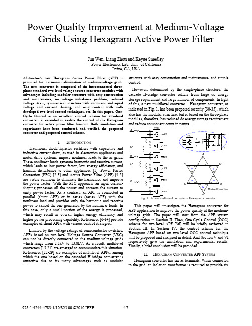
Power Quality Improvement at Medium-Voltage Grids Using Hexagram Active Power FilterJun Wen, Liang Zhou and Keyue SmedleyPower Electronics Lab, Univ. of CaliforniaIrvine, CA, USAAbstract—A new Hexagram Active Power Filter (APF) is proposed for harmonics elimination at medium-voltage grids. The new converter is composed of six interconnected three-phase standard two-level voltage source converter modules with advantages including modular structure with easy construction and maintenance, no voltage unbalance problem, reduced voltage stress, symmetrical structure with automatic and equal voltage and current sharing, and easy control with well-developed two-level control techniques, etc. In this paper, One-Cycle Control – an excellent control scheme for two-level converters is extended to realize the control of the Hexagram converter for active power filter function. Both simulation and experiment have been conducted and verified the proposed converter and proposed control scheme.I.I NTRODUCTIONTraditional diode/thyristor rectifiers with capacitive and inductive current draw, as used in electronics appliances and motor drive systems, impose nonlinear loads to the ac grids. These nonlinear loads generate harmonic and reactive current, which leads to low power factor, low energy efficiency, and harmful disturbance to other appliances [1]. Power Factor Correction (PFC) [2-3] and Active Power Filter (APF) [4-5] are viable solutions to eliminate the harmonics and improve the power factor. With the PFC approach, an input current-shaping processes all the power and corrects the current to unity power factor. As a contrast, an APF is connected in parallel (shunt APF) or in series (series APF) with the nonlinear load and provides only the harmonic and reactive power to cancel the one generated by the nonlinear loads. In this case, only a small portion of the energy is processed, which may result in overall higher energy efficiency and higher power processing capability. References [6-14] provide examples of shunt APFs with various control strategies.Limited by the voltage ratings of semiconductor switches, APFs based on two-level Voltage Source Converter (VSC) can not be directly connected to the medium-voltage grids which range from 2.3kV to 13.8kV. As a result, multilevel converters [15-21] are emerged to accommodate this situation. References [22-29] are examples of multilevel APFs, among which the one based on the cascaded H-bridge converter is attractive due to its many advantages such as modular structure with easy construction and maintenance, and simple control.However, determined by the single-phase structure, the cascade H-bridge converter suffers from large dc energy storage requirement and large number of components. In light of this, a new multilevel converter – Hexagram converter, as indicated in Fig. 1, has been proposed recently [30-35], which also has the modular structure, but is based on the three-phase modules, therefore, has reduced dc energy storage requirementand reduce component count in nature.Fig. 1. A new multilevel converter – Hexagram converter.This paper will investigate the Hexagram converter for APF application to improve the power quality at the medium-voltage grids. The paper will start from the APF system configuration in Section II. Then, One-Cycle Control (OCC) scheme for two-level APF [36] will be briefly reviewed in Section III. In Section IV, the control scheme for the Hexagram APF based on two-level OCC control technique will be proposed and analyzed in detail. And Section V and VI respectively give the simulation and experimental results. Finally, a brief conclusion will be provided.II.H EXAGRAM C ONVERTER APF S YSTEM Hexagram converter has six ac terminals. When connected to the grid, an isolation transformer is required to provide sixterminal three-phase source (neutral floating) or star-connected six-phase source, as indicated by Fig. 2(a) and (b). The primary of the transformer can be either Y-connected or Δ-connected.(a) (b) Fig. 2. Input isolation transformer configurations.(a) Three-phase configuration (neutral floating). (b) Six-phase configuration. This paper will highlight the Hexagram converterconnected to the three-phase transformer as given in Fig. 2(a).In this case, only three phase currents need to be controlled,while at least five phase currents need to be controlled ifconnected to the transformer in Fig. 2(b).Fig. 3. A complete Hexagram converter APF system.A complete system with the Hexagram converter as shunt APF is depicted in Fig. 3. With suitable control, the Hexagram converter will provide the harmonics and reactive currents to the grid so that the source currents are always sinusoidal and at unity power factor regardless of the load condition. III. R EVIEW OF OCCB IPOLARC ONTROL FOR TWO -LEVELAPFThis section will briefly review the OCC control technique for the two-level voltage source converter for the APF applications. Fig. 4 shows the three-phase VSC and its switchingaverage model [36].(a) (b) Fig. 4. Three-phase VSC and its switching average model.(a) Three-phase VSC (b) Switching average model.According to the converter switching average model, the input and output of the converter has the following relationship:2113331211333112333an a bn b cn c dv d v E d v −−⋅=⋅−⎡⎤⎢⎥⎡⎤⎡⎤⎢⎥⎢⎥⎢⎥⎢⎥⎢⎥⎢⎥⎢⎥⎢⎥⎢⎥⎢⎥⎣⎦⎣⎦⎢⎥⎣⎦ (1) where dan, dbn and dcn are respectively the duty ratio signals of the bottom switches San, Sbn and Scn, va, vb andvc are respectively the input voltages of the converter, and E is the output voltage of the converter.One possible solution for (1) is as follows,10.5an a bn bcn c d v d v E d v =−⋅⎡⎤⎡⎤⎢⎥⎢⎥⎢⎥⎢⎥⎢⎥⎢⎥⎣⎦⎣⎦(2)The control goal is to realize the following relationship between the input voltages and source currents,a ab e bc c v i v R i v i =⋅⎡⎤⎡⎤⎢⎥⎢⎥⎢⎥⎢⎥⎢⎥⎢⎥⎣⎦⎣⎦ (3) where Re is the emulated resistance, and ia, ib and ic are the input source currents.Combining (2) and (3) results in the control equation, 121212a an s b m bn c cn i d R i V d i d −⋅=⋅−−⎡⎤⎡⎤⎢⎥⎢⎥⎢⎥⎢⎥⎢⎥⎢⎥⎣⎦⎣⎦ (4) 0.5sm eE R V R ⋅=(5)where Rs is the equivalent current sensing resistance, and Vm is the output of the feedback error compensator.Above control equation can be implemented by OCCcontrol. Fig. 5 depicts the OCC bipolar controller of the two-level VSC for APF application [36]. The source currents are sensed and compared with carrier signals to generate properdriving signals. With OCC control, the harmonics in the three-phase input source currents will be eliminated and unity powerfactor can be achieved.Fig. 5. OCC bipolar controller for two-level APF.Fig. 6 gives a variation of the controller implementation,which senses the load currents and the compensation currentsfrom the APF to duplicate the information of the input sourcecurrents. The result is the same as that can be achieved by thecontroller in Fig. 5.Fig. 6. A variation of OCC bipolar controller for two-level APF.IV.P ROPOSED C ONTROL OF H EXAGRAM APFA.Proposed Control SchemeSimilar as the control of two-level APF, the control goal ofthe Hexagram APF is to compensate the harmonics or reactivecurrents in the source currents caused by the nonlinear loadsand achieve unity power factor at the source side. In addition,the control of Hexagram APF should also ensure that the sixmodules will operate symmetrically and equally share theinput voltage and current. Fig. 7 depicts the proposed controlscheme of the Hexagram APF, which is composed of threetwo-level OCC controllers as indicated by Fig. 6. The firstcontroller senses the phase currents of Module I ia1, ib1, ic1and controls Module I and IV, the second one senses the phasecurrents of Module III ia3, ib3, ic3 and controls Module IIIand VI, and the third one senses the phase currents of ModuleV ia5, ib5, ic5 and controls Module V and II. The threecontrollers share the common load currents informationiA_load, iB_load and iC_load.Refone-cyclecontrol core Error Compensator)A_loadi s RC_loadi s RB_loadi s RA_loadi s RC_loadi s RB_loadi s RA_loadi s RC_loadi s RB_loadi s RFig. 7. Proposed control scheme of Hexagram APF.Take the first controller for illustration, the duty ratiosdan1, dbn1 and dcn1 are respectively generated by comparingthe carrier signals with the summation of the reflected sensedphase currents of Module I ia1/n, ib1/n and ic1/n and thecorresponding load currents iA_load, iB_load and iC_load,and used to drive the bottom switches of Module I San1,Sbn1, Scn1, and the corresponding top switches of Module IVSap4, Sbp4, Scp4. The variable n is the turns ratio of theisolation transformer as indicated in Fig. 3. Thecomplementary signals of the duty ratios dan1, dbn1 and dcn1are respectively used to drive the top switches of Module ISap1, Sbp1, Scp1 and the corresponding bottom switches ofModule IV San4, Sbn4, Scn4. Similarly, the duty ratiosgenerated from the second and third controllers arerespectively used to control the switches of Module III and VIand the switches of Module V and II.The closed-loop dc bus voltage control is realized with theaveraged feedback dc bus voltages of Module I~VI.The control equations in Fig. 7 are as follows, where n isthe turns ratio of the input isolation transformer, R s is theequivalent current sensing resistance, and V m is the output ofthe feedback error compensator.Introducing auxiliary variables to represent the summationof the reflected converter currents from Module I, III and Vand the corresponding load currents,1_11_111_3_33_333_1121121211121121211a A load an s b B load m bn cn c C load a A load an s b B load m bn cn c C load a s i i n d R i i V d n d i i n i i n d R i i V d n d i i n i n R ⋅+−⋅⋅+=⋅−−⋅+⋅+−⋅⋅+=⋅−−⋅+⋅⋅⎡⎤⎢⎥⎡⎤⎢⎥⎢⎥⎢⎥⎢⎥⎢⎥⎢⎥⎢⎥⎣⎦⎢⎥⎣⎦⎡⎤⎢⎥⎡⎤⎢⎥⎢⎥⎢⎥⎢⎥⎢⎥⎢⎥⎢⎥⎣⎦⎢⎥⎣⎦5_55_555_12112121A load an b B load m bn cn c C load i d i i V d n d i i n +−⋅+=⋅−−⋅+⎡⎤⎢⎥⎡⎤⎢⎥⎢⎥⎢⎥⎢⎥⎢⎥⎢⎥⎢⎥⎣⎦⎢⎥⎣⎦(6)1_111_11_3_333_33_5_5551'1''11'1''11'1''a A load a b b B load c c C load a A load a b b B load c c C load a A load a b c i i n i i i i n i i i n i i n i i i i n i i i n i i n i i i ⋅+=⋅+⋅+⋅+=⋅+⋅+⋅+=⎡⎤⎢⎥⎡⎤⎢⎥⎢⎥⎢⎥⎢⎥⎢⎥⎢⎥⎢⎥⎣⎦⎢⎥⎣⎦⎡⎤⎢⎥⎡⎤⎢⎥⎢⎥⎢⎥⎢⎥⎢⎥⎢⎥⎢⎥⎣⎦⎢⎥⎣⎦⎡⎤⎢⎥⎢⎥⎢⎥⎣⎦5_5_1b B loadc C load i i n i i n ⋅+⋅+⎡⎤⎢⎥⎢⎥⎢⎥⎢⎥⎢⎥⎢⎥⎣⎦(7) Then the control equation (6) can be simplified asfollowing:111111333333555555'12'12'12'12'12'12'12'12'12a an s b m bn c cn a an s b m bn c cn a an s b m bn c cn i d R i V d i d i d R i V d i d i d R i V d i d −⋅=⋅−−−⋅=⋅−−−⋅=⋅−−⎡⎤⎡⎤⎢⎥⎢⎥⎢⎥⎢⎥⎢⎥⎢⎥⎣⎦⎣⎦⎡⎤⎡⎤⎢⎥⎢⎥⎢⎥⎢⎥⎢⎥⎢⎥⎣⎦⎣⎦⎡⎤⎡⎤⎢⎥⎢⎥⎢⎥⎢⎥⎢⎥⎢⎥⎣⎦⎣⎦(8)B. Analysis of the Controlled Hexagram APF a) Equivalent module resistor networkTake Module I first for analysis. According to the converter switching average model, by introducing the auxiliary voltage sources va1, vb1 and vc1, the input and output of converter Module I has the following relationship,11111112113331211333112333an a bn b cn c d v d v E d v −−⋅=⋅−⎡⎤⎢⎥⎡⎤⎡⎤⎢⎥⎢⎥⎢⎥⎢⎥⎢⎥⎢⎥⎢⎥⎢⎥⎢⎥⎢⎥⎣⎦⎣⎦⎢⎥⎣⎦(9) where E1 is the dc bus voltage of Module I. From the control equation (8),111111'0.51''an a s bn b m cn c d i R d i V d i =−⋅⎡⎤⎡⎤⎢⎥⎢⎥⎢⎥⎢⎥⎢⎥⎢⎥⎣⎦⎣⎦ (10) Substituting (10) into (9) and using the fact that i a1+i b1+i c1=0 and i A_load +i B_load +i C_load =0 yields, 1111111'0.5''a a s b b m c c v i R E v i V v i ⋅=⋅⎡⎤⎡⎤⎢⎥⎢⎥⎢⎥⎢⎥⎢⎥⎢⎥⎣⎦⎣⎦(11)According to (11), the auxiliary voltages and the auxiliary currents of Module I have a linear relationship; therefore, Module I can be modeled as a resistor network, as indicated by Fig. 8, and the equivalent resistor Re1 satisfies the following equation.110.5se mE R R V ⋅=(12)Fig. 8. Equivalent resistor network representing the relationship betweenthe auxiliary voltage and current of Module I.Module IV has the same control signals as Module I. Due to the symmetrical circuit structure, Module IV can be modeled as the same resistor network as Module I.Similarly, Module III and VI, Module V and II can be respectively modeled as resistor networks as well. 330.5s e mE R R V ⋅=(13) 550.5se mE R R V ⋅= (14) b) Converter current analysisAssume that the three-phase input currents of the Hexagram converter are as follows,135a a b b c c I I I I I I ⎡⎤⎡⎤⎢⎥⎢⎥=⎢⎥⎢⎥⎢⎥⎢⎥⎣⎦⎣⎦(15) Due to the interconnection, the currents inside the Hexagram converter satisfy the following relationships:416325a a b b c c I I I I I I ⎡⎤⎡⎤⎢⎥⎢⎥=−⎢⎥⎢⎥⎢⎥⎢⎥⎣⎦⎣⎦ (16) 122334455661b b a a c c b b a a c c I I I I I I I I I I I I ⎡⎤⎡⎤⎢⎥⎢⎥⎢⎥⎢⎥⎢⎥⎢⎥=−⎢⎥⎢⎥⎢⎥⎢⎥⎢⎥⎢⎥⎢⎥⎢⎥⎢⎥⎢⎥⎣⎦⎣⎦(17)The three-phase currents inside any one module satisfy the following equation:1112223334445556660a b c a b c a b c a b c a b c a b c I I I I I I I I I I I I I I I I I I ++⎡⎤⎢⎥++⎢⎥⎢⎥++=⎢⎥++⎢⎥⎢⎥++⎢⎥++⎢⎥⎣⎦ (18) Limited by the inductors, the circulating current inside the Hexagram converter is low and can be neglected,1234560b a c b a c I I I I I I +++++= (19)Combining the above equations, the phase currents of all the six modules can be derived.14141436363652525221212212a a a b b a b c c c a b c a a a b c b b b c c a b c a a a b b b c c I I I I I I I I I I I I I I I I I I I I I I I I I I I I I I I I I I I ⎡⎤⎡⎤⎡⎤⎢⎥⎢⎥⎢⎥=−=⋅−+−⎢⎥⎢⎥⎢⎥⎢⎥⎢⎥⎢⎥−−+⎣⎦⎣⎦⎣⎦−−⎡⎤⎡⎤⎡⎤⎢⎥⎢⎥⎢⎥=−=⋅⎢⎥⎢⎥⎢⎥⎢⎥⎢⎥⎢⎥−−+⎣⎦⎣⎦⎣⎦−−⎡⎤⎡⎤⎢⎥⎢⎥=−=⋅⎢⎥⎢⎥⎢⎥⎢⎥⎣⎦⎣⎦2c a b c c I I I I ⎡⎤⎢⎥−+−⎢⎥⎢⎥⎣⎦ (20)Similar as (7), introducing auxiliary variables as given below,2_222_22_4_444_44_6_6661'1''11'1''11'''a A load a b b B load c c C load a A load a b b B load c c C load a A l a b c i i n i i i i n i i i n i i n i i i i n i i i n i i n i i i ⎡⎤⋅−⎢⎥⎡⎤⎢⎥⎢⎥⎢⎥=⋅−⎢⎥⎢⎥⎢⎥⎢⎥⎣⎦⎢⎥⋅−⎢⎥⎣⎦⎡⎤⋅−⎢⎥⎡⎤⎢⎥⎢⎥⎢⎥=⋅−⎢⎥⎢⎥⎢⎥⎢⎥⎣⎦⎢⎥⋅−⎢⎥⎣⎦⋅−⎡⎤⎢⎥=⎢⎥⎢⎥⎣⎦6_6____111'1''1oad b B load c C load a A load a b b B load c c C load i i n i i n i i n i i i i n i i i n ⎡⎤⎢⎥⎢⎥⎢⎥⋅−⎢⎥⎢⎥⎢⎥⋅−⎢⎥⎣⎦⎡⎤⋅+⎢⎥⎡⎤⎢⎥⎢⎥⎢⎥=⋅+⎢⎥⎢⎥⎢⎥⎢⎥⎣⎦⎢⎥⋅+⎢⎥⎣⎦(21) Although (7) and (21) describe the instantaneous currents, the corresponding current vectors also satisfy the two equations. Combining (7), (20) and (21) yields,141414363636555''2'1'''''2''''''''''1''2'2''''''''a a a b b a b c c c a b c a a a b c b b b c c a b c a b c I I I I I I I I I I I I I I I I I I I I I I I I I I I I I I ⎡⎤⎡⎤⎡⎤⎢⎥⎢⎥⎢⎥=−=⋅−+−⎢⎥⎢⎥⎢⎥⎢⎥⎢⎥⎢⎥−−+⎣⎦⎣⎦⎣⎦−−⎡⎤⎡⎤⎡⎤⎢⎥⎢⎥⎢⎥=−=⋅⎢⎥⎢⎥⎢⎥⎢⎥⎢⎥⎢⎥−−+⎣⎦⎣⎦⎣⎦⎡⎤⎢⎥=−⎢⎥⎢⎥⎣⎦222''''1''''2'2'a a b c b a b c c c I I I I I I I I I −−⎡⎤⎡⎤⎢⎥⎢⎥=⋅−+−⎢⎥⎢⎥⎢⎥⎢⎥⎣⎦⎣⎦ (22) c) Equivalent converter resistor networkNeglecting the voltages across the inductors, according to the module interconnection, the voltage relationship inside the Hexagram converter is as following:'1122334411665544'3344556633221166'5566112255443322a A A a b b a a c c a a c c a a b b a b B B b c c b b a a b b a a b b c c b c C C c a a c c b b c c b b c c a a cv v v v v v v v v v v v v v v v v v v v v v v v v v v v v v −−−==+++=+++==+++=+++==+++=+++ (23) Above equation can also be used to describe the corresponding voltage vectors.Combining the equivalent resistor networks of Module I~VI as described by (12) ~ (14), the relationship of the auxiliary currents as described by (22) and the relationship of the auxiliary voltages as described by (23), the Hexagram converter can be modeled as a resistor network, as shown in Fig. 9 (a). And Fig. 9 (b) is the simplified circuit.(a) Equivalent resistor network(b) Simplified resistor networkFig. 9. Equivalent resistor network of the Hexagram converter.d) Analysis of the converter resistor network According to Fig. 9 (b), the relationship between the input voltages and the emulated resistors and input currents can be derived as follows, 5513355131531133'3'3'a a e e e e e e e e e e b b c c e e e e e V R R R R R I V R R R R R I V R R R R R I ++−−⎡⎤⎡⎤⎡⎤⎢⎥⎢⎥⎢⎥=−++−⋅⎢⎥⎢⎥⎢⎥⎢⎥⎢⎥⎢⎥−−++⎣⎦⎣⎦⎣⎦ (24)Neglecting the power loss of each converter module, the input power of each converter module is equal to its output power, which yields,***221111111112***223333333332***22555555555('''''')/('''''')/('''''')/a a c c e e b b ma a c c e eb b s a ac c e e b b I I I I I I R E R R V I I I I I I R E R R R R I I I I I I R E R R ⎡⎤⎡⎤⎡⎤++⋅⎢⎥⎢⎥⎢⎥++⋅==⋅⎢⎥⎢⎥⎢⎥⋅⎢⎥⎢⎥⎢⎥++⋅⎣⎦⎣⎦⎣⎦ (25)Simplifying (25) yields,*****12*****32*****53''''''''''''3''''''''2''''3''''''e a a b b c c b c c b s e a ab bc c a c c a m e a a b b c c a b b a R I I I I I I I I I I R R R I I I I I I I I I I V R I I I I I I I I I I ⎡⎤++−−⎡⎤⋅⎢⎥⎢⎥=⋅++−−⎢⎥⎢⎥⎢⎥⎢⎥++−−⎣⎦⎣⎦(26)From (24),1353'3'3'a b c e a e b e c V V V R I R I R I ++=⋅+⋅+⋅(27)Substituting (26) into (27) yields,2***2*3[3('''''')(''')22('''''')(''')]a b cs a ab bc c a b c m a b b c c a a b c V V V R R I I I I I I I I I V I I I I I I I I I ++⋅=⋅++++−++++ (28)In three-phase symmetrical system which contains only positive and negative sequence components,0a b c V V V ++=(29)Combining (28) and (29) yields,****3('''''')(''')2('''''')(''')0a ab bc c a b c a b b c c a a b c I I I I I I I I I I I I I I I I I I ++⋅++−++⋅++=(30)Reorganize (30) gives,*222****'''[3('''''')(''')(''')](''')()(''')0a a c c a c a c a cb b b b b ac a c b b I I I I I I I I I I I I I I I I I I I I I ++−++⋅++⋅+++++⋅++=(31)To satisfy (31), the following relationship must be true.'''0a b c I I I ++=(32)This result indicates that in the three-phase symmetrical system that contains only positive and negative sequencecomponents, the sum of the input currents of the Hexagram converter is zero.e) Hexagram APF control resultsAccording to (32), when the input of the Hexagramconverter is a three-phase symmetrical system, the three input currents of the converter add up to zero.Substituting (32) back to (26) yields, 135e e e e R R R R === (33) And substituting (33) to (24) yields, '6''a a b e b c c V I V R I V I ⎡⎤⎡⎤⎢⎥⎢⎥=⋅⎢⎥⎢⎥⎢⎥⎢⎥⎣⎦⎣⎦(34)Based on (34), the relationship between the input source voltages and currents can be derived.___11661a A load a SA SA e e SB SB b b B load c SC SC c C load I I n V V I V n V nR I I nR I n V V I I I n ⎡⎤⋅+⎢⎥⎡⎤⎡⎤⎡⎤⎢⎥⎢⎥⎢⎥⎢⎥⎢⎥=⋅=⋅⋅+=⋅⎢⎥⎢⎥⎢⎥⎢⎥⎢⎥⎢⎥⎢⎥⎢⎥⎣⎦⎣⎦⎣⎦⎢⎥⋅+⎢⎥⎣⎦(35) This result indicates that the input source currents will be in phase with the corresponding source voltages under the proposed control scheme.Substituting (32) to (22) yields, 513246135246513246'''''''''''''''''''''a a a a a a a b b b b b b b c c c c c c c I I I I I I I I I I I I I I I I I I I I I ⎡⎤⎡⎤⎡⎤⎡⎤⎡⎤⎡⎤⎡⎤⎢⎥⎢⎥⎢⎥⎢⎥⎢⎥⎢⎥⎢⎥===−=−=−=⎢⎥⎢⎥⎢⎥⎢⎥⎢⎥⎢⎥⎢⎥⎢⎥⎢⎥⎢⎥⎢⎥⎢⎥⎢⎥⎢⎥⎣⎦⎣⎦⎣⎦⎣⎦⎣⎦⎣⎦⎣⎦ (36) Combining (7), (21), (35) and (36) yields,_513246135246_513246_SA A load a a a a a a a SB b b b b b b b B load c c c c c c c SC C load I I I I I I I I I I I I I I I I n I I I I I I I I I I I ⎡⎤−⎡⎤⎡⎤⎡⎤⎡⎤⎡⎤⎡⎤⎡⎤⎢⎥⎢⎥⎢⎥⎢⎥⎢⎥⎢⎥⎢⎥⎢⎥⎢⎥===−=−=−==⋅−⎢⎥⎢⎥⎢⎥⎢⎥⎢⎥⎢⎥⎢⎥⎢⎥⎢⎥⎢⎥⎢⎥⎢⎥⎢⎥⎢⎥⎢⎥−⎣⎦⎣⎦⎣⎦⎣⎦⎣⎦⎣⎦⎣⎦⎢⎥⎣⎦(37)This result indicates that the input currents of the Hexagram converter are the compensation currents equal to the subtraction of the sinusoidal source currents and the non-linear load currents. Besides, Module I, III and V of theHexagram converter have the same phase currents as the inputcurrents of the converter, while Module II, IV and VI have the reversed ones.Based on (11) ~ (14), (33) ~ (34) and (36), 513246135246513246'11'66'a a a a a a a a SA e SB b b b b b b b b c c c c c c c c SC V V V V V V I V V V V V V V V R I V V n V V V V V V I V V ⎡⎤⎡⎤⎡⎤⎡⎤⎡⎤⎡⎤⎡⎤⎡⎤⎡⎤⎢⎥⎢⎥⎢⎥⎢⎥⎢⎥⎢⎥⎢⎥⎢⎥⎢⎥===−=−=−=⋅=⋅=⋅⎢⎥⎢⎥⎢⎥⎢⎥⎢⎥⎢⎥⎢⎥⎢⎥⎢⎥⎢⎥⎢⎥⎢⎥⎢⎥⎢⎥⎢⎥⎢⎥⎢⎥⎢⎥⎣⎦⎣⎦⎣⎦⎣⎦⎣⎦⎣⎦⎣⎦⎣⎦⎣⎦ (38) This result indicates that the six modules inside the Hexagram converter equally share the input voltages of the converter.From (12) ~ (14) and (33), 123456E E E E E E ===== (39)This indicates that the six dc bus voltages of the Hexagram converter are the same.Equations (35) and (37) ~ (39) give the results of the Hexagram APF with the proposed control scheme in Fig. 7when the input of the Hexagram converter is the three-phase symmetrical system containing no zero sequence componentsas described by (29). This condition is the most likelyoperation condition of the Hexagram converter, since thevoltages supplied by a symmetrical three-phase transformer do not contain any zero sequence components but positive andnegative sequence components no matter how the grid isunbalanced. With the proposed control scheme, the Hexagramconverter will compensate the non-linear load currents so that the input source currents will be sinusoidal and in phase withthe corresponding source voltages. Besides, the six modules of the converter have the same phase currents, the same averageinput voltages, the same dc bus voltages and thus the same power as well. The input voltage of each module is one sixthof that of the converter so that the voltage stress of the semiconductor switches is reduced to one sixth. The instantaneous power through each module is constant. When the transformer has some asymmetry, the equivalent source voltages of the Hexagram converter will contain some zero-sequence components. Under this condition, theconverter behavior will still follow the rules described by the voltage equation in (24) and the energy equation in (25).When the zero-sequence components are small, the results areclose to the derived equations (35) and (37) ~ (39) under thesymmetrical systems.V. S IMULATION V ERIFICATIONA 1MW 4.16kV Hexagram APF system has been built inPSIM7.0. The non-linear load is composed of a three-phase diode rectifier with load at 40Ω. The Hexagram converter has eighteen inductors at 1mH each (three inductors per module). The dc bus capacitor for each module is 820μF each. The turns ratio of the isolation transformer for the Hexagram converter is 1:1, and the secondary windings of the transformer is configured as a six-terminal three-phase voltage source with neutral floating. The switching frequency of the Hexagram converter is 10 kHz.Fig. 10 shows the simulation results. Fig. 10 (a) shows the input source voltages VSA, VSB, VSC, input source currentsISA, ISB, ISC, load currents IA_load, IB_load, IC_load, and the currents from the Hexagram converter IA_APF, IB_APF,IC_APF. With the compensation currents from the Hexagramconverter, the source currents are sinusoidal and in phase withthe corresponding source voltages. Fig. 10 (b) shows the currents of the Hexagram converter IA_APF, IB_APF, IC_APF, currents of Module I Ia1, Ib1, Ic1 and currents of Module IV Ia4, Ib4, Ic4. The currents of Module I are the same as the currents of the Hexagram converter, while the currents of Module IV are reversed. The other four moduleshave the similar results. Fig. 10 (c) shows the six dc bus voltages, which are identical and are at 1300V. Fig. 10 (d)shows the input line voltages VA-VB and the line voltages ofModule I Va1-Vb1. The input line voltage is six times the line voltages of Module I, and other modules have similar result. Since the voltage of one module is only one sixth of the input voltage, the voltage stress of the converter is reduced to one sixth compared to a single two-level VSC at the same input voltage. The simulation results have well verified the proposed Hexagram APF and proposed control scheme.(a) Source voltages, source currents, load currents and currents fromHexagram converter(b) Currents of Hexagram converter, Module I and Module IV(c) Six dc bus voltages(d) Line voltages of Hexagram converter and line voltages of Module IFig. 10. Simulation results of 1MW Hexagram APF system.VI.E XPERIMENTAL VERIFICATIONA 1kW Hexagram converter prototype has been built for verification. The prototype has eighteen inductors at 1.5mH each and six dc bus capacitors at 470μH each. The nonlinear load is composed of a three-phase diode rectifier and a 40Ωresistor. The isolation transformer of the Hexagram converter is 3:1. The switching frequency of the converter is 16 kHz.Fig. 11 shows the experimental results. Fig. 11 (a) shows the input source voltage VSA and three-phase input source currents ISA, ISB, ISC. The input source voltage is 80V line-to-neutral RMS, and the input source currents are 4A RMS. The input source currents are in phase with the corresponding source voltages. Fig. 11 (b) shows the input source voltage VSA, input source currents ISA, load current IA_load and the current from the Hexagram converter IA_APF. With the compensation currents from the Hexagram converter, the input source currents are sinusoidal and in phase with the corresponding source voltages. Fig. 11 (c) shows the input phase voltage VAA' and the three-phase input currents Ia, Ib and Ic of the Hexagram converter. Since the turns ratio of the isolation transformer is 3:1, the input phase voltage of the Hexagram converter is 240V RMS. Fig. 11 (d) and (e) respectively shows the input phase voltage VAA' of the Hexagram converter with the currents of Module I Ia1, Ib1, Ic1 and the currents of Module IV Ia4, Ib4, Ic4. The currents of Module I are the same as the input currents of the Hexagram converter, while the currents of Module IV are in the reversed direction. The currents of the other four modules have similar results. Fig. 11 (f) shows the input line voltage VAA'-VBB' of the converter and the corresponding line voltage of Module I Va1b1. The input line voltage is around 420V RMS, and the line voltage of Module I is around 70V. Correspondingly, the input phase voltage is 240V and the phase voltage of Module I is 40V. The voltage of one module is one sixth of the input voltage, so that the voltage stress of the semiconductor switches is reduced to one sixth. Fig. 11 (g) shows the six dc bus voltages, which are identical and are controlled at 170V each.The experimental results have fully verified the Hexagram APF and the proposed control scheme. With the proposed control scheme, the currents from the Hexagram converter compensate the non-linear load currents, and the input source currents are in phase with the corresponding input sourcevoltages. The voltage stress of the converter is reduced to onesixth and the six modules equally share the output power.(a) Source voltage and currents(b) Source voltage, source current, load current and current fromHexagram converter(c) Input voltage and currents of Hexagram converter(d) Input voltage of Hexagram converter and currents of Module I(e) Input voltage of Hexagram converter and currents of Module IV(f) Input line voltage of Hexagram converter and line voltage of Module I(g) Six dc bus voltagesFig. 11. Experimental results of 1kW Hexagram APF system.。

高三英语学术研究方法创新不断练习题40题答案解析版1. When conducting academic research, if you want to find the most relevant literature in a specific field, which of the following is the most important step in using a literature database?A. Entering random keywordsB. Using broad and general keywordsC. Selecting accurate and specific keywordsD. Ignoring the keyword search function and browsing randomly答案:C。
解析:在学术研究中,当使用文献数据库时,选择准确和具体的关键词是最重要的步骤。
如果输入随机关键词(A选项),可能会得到大量不相关的文献。
使用宽泛和笼统的关键词((B选项)会导致结果过于繁杂且相关性不强。
而完全忽略关键词搜索功能随机浏览((D 选项)效率极低,难以找到特定领域最相关的文献。
2. In academic research, which type of literature database is more likely to provide in - depth and specialized research articles?A. General - purpose databasesB. Social media platformsC. Specialized databases in the research fieldD. Public libraries' general collections答案:C。
解析:在学术研究中,专门针对研究领域的专业数据库更有可能提供深入和专业的研究文章。

用一种好方法的英文In today's fast-paced and technology-driven world, finding effective ways to accomplish tasks is crucial. We are constantly seeking efficient methods to make our lives easier and more productive. This desire extends to every aspect of our lives, from work to personal endeavors. In this article, we will explore a variety of good methods that can help us achieve our goals effectively and efficiently.Time Management T echniquesOne of the most valuable skills we can develop is effective time management. With so much to do and limited time, utilizing good time management techniques can make a significant difference in our productivity.Pomodoro T echniqueThe Pomodoro Technique, developed by Francesco Cirillo in the late 1980s, is a time management method that divides work into intervals, typically 25 minutes in length, separated by short breaks. After four consecutive work intervals, a longer break is taken. This technique helps maintain focus and avoid burnout by balancing work and rest periods. Eisenhower MatrixThe Eisenhower Matrix, also known as the Urgent-Important Matrix, is a decision-making tool that helps prioritize tasks based on their urgency and importance. By dividing tasks into four categories: urgent/important,important/not urgent, urgent/not important, and not urgent/not important, we can focus on high-priority tasks and eliminate or delegate less critical ones.Learning TechniquesLearning is a lifelong process, and finding effective ways to acquire new knowledge and skills is essential for personal and professional growth. Spaced RepetitionSpaced repetition is a learning technique that involves reviewing information with increasing intervals of time in between. This method is based on the psychological spacing effect, which suggests that learning is more effective when there are gaps between review sessions. By spacing out reviews, we strengthen our long-term memory and retain information for a longer period.Active LearningActive learning is a teaching method that engages learners in the learning process through activities, discussions, and problem-solving. This approach encourages deeper understanding, critical thinking, and knowledge retention. By actively participating in the learning process, learners become more involved and motivated, resulting in better outcomes.Productivity TechniquesIncreasing productivity is a common goal for individuals andorganizations. Implementing good productivity techniques can help us accomplish more in less time.The 80/20 Rule (Pareto Principle)The 80/20 Rule, also known as the Pareto Principle, suggests that 80% of the results come from 20% of the efforts. By identifying and focusing on the most important tasks that yield the greatest results, we can maximize our productivity. This technique involves prioritizing tasks based on their impact and allocating resources accordingly.Task BatchingTask batching involves grouping similar tasks or activities together to streamline workflow and optimize productivity. By focusing on one type of task at a time, we reduce time wasted on context switching and increase efficiency. For example, responding to emails and making phone calls within a designated time frame rather than sporadically throughout the day.ConclusionUsing good methods and techniques is vital to achieving our goals effectively and efficiently. Whether it's managing time, learning new skills, or increasing productivity, there are numerous approaches to help us succeed. By adopting these techniques and incorporating them into our daily lives, we can maximize our potential and lead more satisfying andproductive lives. Remember, finding the right method is a personal journey, and experimentation is key. So, go ahead and explore these techniques to find what works best for you!。

高中英语科技论文翻译单选题40题答案解析版1.The term “artificial intelligence” is often abbreviated as _____.A.AIB.IAC.AIID.IIA答案:A。
“artificial intelligence”的常见缩写是“AI”。
B 选项“IA”并非此词组的缩写。
C 和D 选项都是错误的组合。
2.In a scientific research paper, “data analysis” can be translated as _____.A.数据分析B.数据研究C.数据调查D.数据理论答案:A。
“data analysis”的正确翻译是“数据分析”。
B 选项“数据研究”应为“data research”。
C 选项“数据调查”是“data survey”。
D 选项“数据理论”是“data theory”。
3.The phrase “experimental results” is best translated as _____.A.实验结论B.实验数据C.实验结果D.实验过程答案:C。
“experimental results”的准确翻译是“实验结果”。
A 选项“实验结论”是“experimental conclusion”。
B 选项“实验数据”是“experimental data”。
D 选项“实验过程”是“experimental process”。
4.“Quantum mechanics” is translated as _____.A.量子物理B.量子力学C.量子化学D.量子技术答案:B。
“Quantum mechanics”是“量子力学”。
A 选项“量子物理”是“quantum physics”。
C 选项“量子化学”是“quantum chemistry”。
D 选项“量子技术”是“quantum technology”。

华中科技大学硕士学位论文ZVS三电平DC/DC变换器的研究姓名:李小兵申请学位级别:硕士专业:电力电子与电力传动指导教师:李晓帆20060428摘 要直流变换器是电力电子变换器的重要组成部分,软开关技术是电力电子装置向高频化、高功率密度化发展的关键技术,成为现代电力电子技术研究的热点之一。
由于对电源设备电磁兼容的要求的提高,一般在电源设备中都要加入功率因数校正环节,导致后继开关管电压应力的提高。
三电平直流变换器相应提出,主开关管的电压应力为输入直流电压的一半。
使得三电平直流变换器一提出就得到全世界电源专家和学者的重视,短短十几年内,相继提出许多种改进型三电平直流变换器,包括半桥式和全桥式。
根据主开关管实现软开关的不同,将三电平直流变换器分为零电压软开关和零电压零电流软开关。
本文首先给出了基本半桥式三电平DC/DC变换器,详细分析了其工作原理,讨论了主要参数的设计和由于次级整流二极管的反向恢复导致主开关管的电压尖峰。
接着给出一种带箝位二极管的改进型半桥式三电平DC/DC变换器。
文中给出了Saber软件的仿真结果,进一步证明改进方案的正确性和可行性。
针对前面讨论的两种半桥式三电平DC/DC变换器,设计了实验电路来验证理论分析的正确性,文中给出了实验结果。
接着研究了一种新型ZVS三电平LLC谐振型DC/DC变换器,文中详细讨论了该变换器的工作原理,讨论了主要参数的设计过程,给出了仿真结果。
最后,设计了一台实验装置来验证理论分析的正确性,给出了实验结果,说明了主开关管可以在全负载范围内实现零电压软开关,变换器的效率在输入电压高端较高,并且次级整流二极管实现了零电流开关,二极管电压应力为输出电压的2倍。
本文通过理论分析、仿真研究和实验验证,证实了半桥式三电平DC/DC变换器的优越性能,改进型的半桥式三电平DC/DC变换器比较好地消除了主开关管上的电压尖峰。
ZVS三电平LLC谐振型DC/DC变换器良好的性能,使得在有掉电维持时间限制的场合得到广泛应用。
How to Reduce the Spike Voltage forSynchronous Rectifier Buck ConverterBY James Yeh and Hunter HoAbstractSynchronous rectifier buck operation in high switch frequency will generate the spike voltage and ringing due to the stray inductance and capacitance exist in practical PCB. In this paper will discuss the source of the spike voltage in detail and how to select and design suitable snubber circuit to decrease it. Theoretical analysis, simulation and experimental result could provide some information, for related engineer.1.I ntroductionSynchronous rectifier buck is widely used in the power supply of many electronic equipment, due to it has fast response, simple topology, higher efficiency for a low voltage and high current need. But it still has a serious problem “EMI”. While the switch turn on and turn off in a high frequency, the stray inductance and capacitance exist in practical PCB, it will generate high frequency ringing and spike voltage. The high frequency ringing and spike voltage will interference the equipment or damage the switch. In order to solve this problem, there are some methods such as “soft switching”, “snubber circuit”, and ”add EMI filter”. In this paper, we will discuss what cause spike and ringing in detail, and how to place a simple passive component (snubber circuit) to solve this drawback.2.Sourse analysis of spike voltage and how to suppressFigure 1 shows a typical synchronous rectifier Buck converter, where Ls1 and Ls2 are the stray inductance due to the finite size of the circuit layout. In practical circuits operation, while the Vg2 signal has been low and Vg1 has not reach high yet, it is called the dead time. The load current flows through the body diode D2 and stray inductance Ls2. During the dead time, item the Vg1 has been already high, then the M1 has been turned on and D2 start to add reverse voltage. But the body diode with reverse voltage exist a reverse recovery current (I rr), it practical turn off has to across a reverse recovery time (t rr) and has the snap-off current during the extremely short time t s. The snap-off body diode current as show in Figure 2 can produce the transient high peak voltage, and ringing. It may be generate EMI to inference the controller or others equipment and the high peak voltage may be to damage the MOSFET (M2). For different position of stray inductance, a high frequency capacitor (Cd) and RC Snubber circuit must be placed across the drain of M1 to ground and lower switch (M2) of the synchronous rectifier buck converter, respectively, to reduce the peak voltage and to damp the ringing. The circuit as shows in Figure 3. Although the spike and the ringing are due to snap-off current of body diode (D2), accordingto the different position of stray inductance, we can provide the different solution. Find a proper capacitance (Cd) is enough to decrease the spike and ringing, if there is only L s1 in circuit. But if the L s2 is existence simultaneously, the snubber circuit (Rs-Cs) must be placed across the low-side MOSFET (M2) to protect the Mosfet and damp the ringing. It will be discussed in the different situation and solved as below:VdD1RLFigure 1. Typical Synchronous Rectifier Buck converteri D2tFigure 2. Body diode currentVdD1RLFigure 3. Synchronous Rectifier Buck converter with high frequencyinput capacitor and R-C snubber circuitCase 1:First, assume the stray inductance 02»s L , at the instant of body diode reverse-recovery current snap off, the equivalent circuit as shows in Figure 4, Cp is the stray capacitance includes the junction capacitance of the switch and stray capacitance due to circuit layout and mounting. For analyzing this equivalent circuit the instant of diode snap-off is treated as t=0. The initial inductor current is Irr as showed in Figuere2 and initial capacitor voltage iszero. While the body diode snap-off the d ss phase V t IrrL V +=1, it is a large value of spike voltage at the instant, and the Ls1 and Cp will generate high frequency ringing. Theoscillated frequency is p s o C L 11=w , it is damped by only equivalent- series -resister (ESR). In this case, we could place the high frequency capacitor (Cd), and enough to decrease the spike and ringing. Figure 5 shows the equivalent circuit of converter with the high frequency input capacitance, and the initial capacitance voltage of Cd is Vd, so Cdmust has capability to provide Qrr. The 2rr rr rr tI Q =, andd rr V QCd 10>: (1)Ls1Cp-Figure 4. Body diode snap-off equivalent circuitLs1Cp-Figure 5. Body diode snap-off equivalent circuit with high frequency input capacitor.In the component selection of Cd, at least one low ESR capacitor should be used to provide good performance. Here, to adopt either the ceramic or the tantalum type is suitable, and it should be as close to M1 (up-side Mosfet) as possible when layout.Example 1. Consider Figure 3.circuit, assume Io=10A, Ls1=1nH, Ls2=0, Vd=12V, Vo=5V,L1=10m H, Cin=C L =1000m F, f s =100kHz , body diode trr=19nS, Irr=78A Figure 6 shows the wave of Vphase that is simulated by Pspice. While thebody diode reverse recovery, the Vphase has a 30 V spike voltage.TimeV(R2:2)(IS(M3)+IB(M3))-100A0A100ASEL>>IrrFigure 6.The wave of Vphase that is simulated by Pspice. While the body diode snap-offIn order to reduce spike, we add a capacitor Cd. According equation (1), Cd=0.1m F. The simulated result is shown in Figure 7. Figure 8 shows the simulated result which theCd=1m F, According to simulated result, we can see a greater value of Cd with a better capability to reduce spike voltage. Here, the Cd is also an EMI filter.Time8.01992ms8.01996ms8.02000ms8.02004ms 8.02008ms8.02012ms8.02016msV(R2:2)0V10V20V30VVphase(IS(M3)+IB(M3))-100A0A100ASEL>>IrrFigure 7. The simulated result which Cd=0.1m ..Time8.01992ms8.01996ms 8.02000ms 8.02004ms 8.02008ms 8.02012ms 8.02016msV(R2:2)10V20V30V-2VSEL>>Vphase(IS(M3)+IB(M3))-100A0A100AIrrFigure 8. The simulated result which the Cd=1mCase 2:Assume 01»s L , the equivalent circuit is the same as Figure 4. But in this case should be added a snubber circuit to decrease the spike voltage across M2, the equivalent circuit is shown in Figure 6.RsCsFigure 9. Body diode snap-off equivalent circuit with R-C snubberIn this two-order transient circuit, the initial inductor current is Irr and the initial capacitor voltage is zero, at t=0. The differential equation of the body diode voltage and the boundary condition are as showed below:d df df ss df ss V t V dtt dV C R dtt V d C L -=++)()()(22 (2)s rr df R I V -=+)0( (3)222)0(s s rr s d s s rr df L R I L V R C I dtdV ---=+ (4)The solution of equation (2) is)cos()cos()(2g f w j a ----=-t e I C L V t V a t rrs s d df (5)where2021w a w -=a , 02w a s R = , )2/("tan 21rr s a s rr d I L R I V w f -=-, and )(tan 1a w g a -= (6)In equation (5), the maximum voltage across body diode can be found by setting the derivative 0/)(=dt t dV df , and we can get m t which is the maximum voltage time.02³-+=am t w p g j (7)To substitute t=t m into equation (4) and define 22)/(d rr s base V I L C =, rr d base I V R /= we can get the maximum reverse voltage which across the low side Mosfets M2 as shown in equation (8).tm bases base s s base d e R RR R C C V V a --+++=])(75.01[13max (8)From equation (8), we can detect the oscillations are damped out by R s and the maximumvoltage is depended on the values of Rs and Cs.The energy loss in the resistor is2222121d s rr s R V C I L W += (9)The energy stored in Cs is equal to221d s C V C W = (10)The total energy dissipation is22221d s rr s Cs R tot V C I L W W W +=+= (11)The above design equation is too complex. In most cases a simple design technique is need to determine suitable values for the snubber components (Rs and Cs). Here, we introduce a simple method. First select a snubber capacitor with a value that is 4-10 times larger than the estimated capacitance of the synchronous switch (M2) and which mountingcapacitance. Rs is selected so that od I VRs =. This means that the initial voltage step due tothe current flowing in Rs is no greater than the clamped input voltage. The dissipated power in Rs can be estimated from peak energy stored in Cs:s d s diss f V C P 2» (12)wherefs is the switch frequency.Example 2. To consider the same conditions of example 1, the difference is Ls1=0 andLs2=0.5nH. Figure 10 shows the body diode reverse recovery current and voltage across the synchronous switch (M2), it exist a 35 V spike voltage.Time8.0699800ms8.0700000ms8.0700200ms8.0700400ms8.0700600ms8.0700800ms8.0699694ms V(L2:1)102030(IS(M3)+IB(M3))-50A0A50A-94ASEL>>Figure 10.The body diode reverse recovery current and voltage across thesynchronous switch (M2), in Ls2=0.5nHIn order to decrease this spike voltage, we can add the Rs=1 Ω, and Cs=0.1m F .The result of simulation is shown in Figure 11.The spike voltage has been suppressed to 23V,and the ringing has been reduced, too. AS the amount of Cs increase , the spike voltage will reducefurther. However, the total energy dissipation increases linearly with Cs.Time 8.0599800ms8.0600000m s 8.0600200ms 8.0600400ms8.0600600ms 8.0600800ms 8.0601000ms 8.0601200ms8.0599616ms V (L2:2)10V20V30V-2VSEL>>Vph ase(IS(M3)+I B(M3))-100A0A100AIrrFigure 11. The result of simulation which is added thesnubber circuit (Rs=1 Ω, and Cs=0.1m F ).Case 3:Assume Ls1 and Ls2 are exist simultaneously, as shows in Figure3. Adding Cd to decrease the ringing and noise of V phase and filter high frequency noise , moreover adding the snubber circuit (Rs-Cs) will suppress the spike voltage across the synchronous switch (M2).Sometimes we need to sense the Vphase signal, then the serious ringing and spike voltage will influence normal operation of the control IC. Adding a high frequency capacitor Cd, will not able to reduce the ringing that is due to stray inductance Ls2. In this case, adding a suitable snubber circuit can get a better performance.3.Experimental ResultsThe following a practical design example is for further understand the snubber.The experimental circuit is shown in Figure3.The parameters are Vd=5V, Vo=2.5V, Io=5A, L1=7.8m H, Cin= 3000m F, C L =1680m F, M1and M2 are Philips ’s 66NQ03LT, and control IC is RT9202 which is made by RichTek. We are measured the stray inductances L s1= 0.1nH, L s2=0.2nH. For how to measure the stray inductance, we provide a simple method. At first, measure the drain to source voltage ringing cycle (T1) of the synchronous switch (M2), then to add a known capacitor C test in parallel with the switch and finally re-measuring the period (T2). The L s1+L s2 can be get from:)41)((212221tests s st C T T L L L p -=+= (13)Usually C test is approximately equal to twice the switch capacitance. Next, adding a large Cd to decouple the influence of L s1, and follow the above method to measure again to get the L s2, then L s1=L st -L s2.Figure 12 shows a practical measured wave of the V phase and the voltage across thesynchronous rectifier switch (M2) without any snubber circuit. According to Figure 12 we can tell the ringing is very serious, and the efficiency of converter is 89%. Figure 13 shows the wave which only adding Cd=3m F, the ringing will not improve further due to the Ls2 existence. For reduce the ringing in Vphase, consider adding snubber circuit (Rs=1Ω,Cs=0.01m F). Figure 14 shows the wave which circuit have been added the snubber without adding Cd. Then observation, the ringing and spike voltage have been reduced, and in this condition the efficiency of converter is also 88%. Figure 15 shows the same wave which Cd=3m F, and the snubber circuit (Rs=1Ω, Cs=0.01m F), its efficiency is 88%. We find the ringing and spike voltage have been reduced. Figure16, 17,18 and 19 shows the same wave, the difference is load current Io=20A.V phaseV DS2I DS2Figure 12 The wave of Vphase and the voltage across the synchronousrectifier switch (M2) without snubber.(CH1:2A/div, Ch2: 10V/div, Ch3:1V/div,t:40ns/div)V PHASEV DS2I DS2Figure 13. The wave of Vphase and the voltage across the synchronousrectifier switch (M2) which is added .Cd=3m F(CH1:2A/div, Ch2: 10V/div, Ch3:1V/div,t:40ns/div)V PHA SEV DS2I DS2Figure 14. The wave of Vphase and the voltage across the synchronous rectifier switch (M2) which is added snubber circuit(Rs=1Ω, Cs=0.01m F)(CH1:2A/div, Ch2: 10V/div, Ch3:1V/div,t:40ns/div)V p h a s eV D S2I D S2Figure 15.The wave of Vphase and the voltage across the synchronous rectifier switch (M2) which is added snubber circuit(Rs=1Ω, Cs=0.01m F) and Cd=3m F(CH1:2A/div, Ch2: 10V/div, Ch3:1V/div,t:40ns/div)VphaseVDS2IDS2Figure.16 The wave of Vphase and the voltage across the synchronous rectifier switch (M2) without snubber. When Io=20A(CH1:2A/div, Ch2: 2V/div, Ch3:1V/div,t:80ns/div)VphaseVDS2IDS2F17 The wave of Vphase and the voltage across the synchronous rectifier switch (M2) which is added .Cd=3m F When Io=20A (CH1:2A/div, Ch2: 2V/div, Ch3:1V/div,t:80ns/div)VphaseVDS2IDS2F18 The wave of Vphase and the voltage across the synchronous rectifier switch (M2) which is added snubber circuit(Rs=1Ω, Cs=0.01m F) When Io=20A(CH1:2A/div, Ch2: 2V/div, Ch3:1V/div,t:80ns/div)VphaseVDS2IDS2F19 The wave of Vphase and the voltage across the synchronous rectifier switch (M2) which is added snubber circuit(Rs=1Ω, Cs=0.01m F) and Cd=3m F When Io=20A(CH1:2A/div, Ch2: 2V/div, Ch3:1V/div,t:80ns/div)For efficiency consideration, adding snubber circuit cannot improve the total energy loss of converter further. Because the energy loss due to the reverse recovery current of body diode has been transmit to snubber resistance (Rs). But it is really effective to restrict the voltage spike. In this way, we can reduce power device rating, and improve the EMI, output noise.4.ConclusionOne of the primary reasons for using snubbers is the presence of the stray inductance in the circuit that generate voltage spikes and ringing when excited by the switching action and diode turn off. Larger stray inductance means larger snubber components and more dissipation. As power levels rise, this becomes progressively more important because of the increasing di/dt. So before actually designing the snubber, it is important to minimize the circuit stray inductance and take good care of circuit layout.Reference[1] William McMurray, “ Optimum Snubbers for Power Semiconductors”, IEEE IASTransactions, Vol. IA-8, No,5, Sep/Oct 1972,pp. 593-600.[2] Jim Hagerman and Hagerman Technology, “Calculating Optimum Snubbers”.[3] Rudy Severns ”Design of Snubbers for Power Circuit”.[4] Mohan, Undeland, and Robbins, “ Power electronics Converters, Applications, andDesign”.。
Dual, 16-Bit, 1000 MSPS,TxDAC+ Digital-to-Analog ConverterAD9125 Rev. 0Information furnished by Analog Devices is believed to be accurate and reliable. However, noresponsibility is assumed by Analog Devices for its use, nor for any infringements of patents or other rights of third parties that may result from its use. Specifications subject to change without notice. No license is granted by implication or otherwise under any patent or patent rights of Analog Devices. T rademarks and registered trademarks are the property of their respective owners. One Technology Way, P.O. Box 9106, Norwood, MA 02062-9106, U.S.A. Tel: 781.329.4700 Fax: 781.461.3113 ©2010 Analog Devices, Inc. All rights reserved.FEATURESFlexible CMOS interface allows dual-word, word, or byte load Single-carrier W-CDMA ACLR = 80 dBc at 122.88 MHz IF Analog output: adjustable 8.7 mA to 31.7 mA, R L = 25 Ω to 50 Ω Novel 2×/4×/8× interpolator/complex modulator allows carrier placement anywhere in the DAC bandwidthGain and phase adjustment for sideband suppression Multichip synchronization interfaceHigh performance, low noise PLL clock multiplierDigital inverse sinc filterLow power: 900 mW at 500 MSPS, full operating conditions 72-lead, exposed paddle LFCSPAPPLICATIONSWireless infrastructureW-CDMA, CDMA2000, TD-SCDMA, WiMAX, GSM, LTEDigital high or low IF synthesisTransmit diversityWideband communications: LMDS/MMDS, point-to-point Cable modem termination systems GENERAL DESCRIPTIONThe AD9125 is a dual, 16-bit, high dynamic range TxDAC+® digital-to-analog converter (DAC) that provides a sample rate of 1000 MSPS, permitting a multicarrier generation up to the Nyquist frequency. It includes features optimized for direct conversion transmit applications, including complex digital modulation, and gain and offset compensation. The DAC outputs are optimized to interface seamlessly with analog quadrature modulators, such as the ADL537x F-MOD series from Analog Devices, Inc. A 4-wire serial port interface allows programming/readback of many inter-nal parameters. Full-scale output current can be programmed over a range of 8.7 mA to 31.7 mA. The AD9125 comes in a72-lead LFCSP.PRODUCT HIGHLIGHTS1.Ultralow noise and intermodulation distortion (IMD)enable high quality synthesis of wideband signals frombaseband to high intermediate frequencies.2. A proprietary DAC output switching technique enhancesdynamic performance.3.The current outputs are easily configured for varioussingle-ended or differential circuit topologies.4.The flexible CMOS digital interface allows the standard32-wire bus to be reduced to a 16-wire bus.TYPICAL SIGNAL CHAINCOMPLEX BASEBANDDCCOMPLEX IFf IFRFLO – f IF916-1Figure 1.AD9125Rev. 0 | Page 2 of 56TABLE OF CONTENTSFeatures .............................................................................................. 1 Applications ....................................................................................... 1 General Description ......................................................................... 1 Product Highlights ........................................................................... 1 Typical Signal Chain ......................................................................... 1 Revision History ............................................................................... 2 Functional Block Diagram .............................................................. 3 Specifications ..................................................................................... 4 DC Specifications ......................................................................... 4 Digital Specifications ................................................................... 5 Latency and Power-Up Timing Specifications ......................... 5 AC Specifications .......................................................................... 6 Absolute Maximum Ratings ............................................................ 7 Thermal Resistance ...................................................................... 7 ESD Caution .................................................................................. 7 Pin Configuration and Function Descriptions ............................. 8 Typical Performance Characteristics ........................................... 10 Terminology .................................................................................... 16 Theory of Operation ...................................................................... 17 Serial Port Operation ................................................................. 17 Data Format ................................................................................ 17 Serial Port Pin Descriptions ...................................................... 17 Serial Port Options ..................................................................... 18 Device Configuration Register Map ............................................ 19 Device Configuration Register Descriptions .......................... 21 CMOS Input Data Ports ................................................................ 29 Dual-Word Mode ....................................................................... 29 Word Mode ................................................................................. 29 Byte Mode .................................................................................... 29 Interface Timing ......................................................................... 30 FIFO Operation .......................................................................... 30 Digital Datapath .............................................................................. 32 Premodulation ............................................................................ 32 Interpolation Filters ................................................................... 32 NCO Modulation ....................................................................... 35 Datapath Configuration ............................................................ 35 Determining Interpolation Filter Modes ................................ 36 Datapath Configuration Example ............................................ 37 Data Rates vs. Interpolation Modes ......................................... 38 Coarse Modulation Mixing Sequences .................................... 38 Quadrature Phase Correction ................................................... 39 DC Offset Correction ................................................................ 39 Inverse Sinc Filter ....................................................................... 39 DAC Input Clock Configurations ................................................ 40 DAC Input Clock Configurations ............................................ 40 Analog Outputs............................................................................... 42 Transmit DAC Operation .......................................................... 42 Auxiliary DAC Operation ......................................................... 43 Baseband Filter Implementation .............................................. 44 Driving the ADL5375-15 .......................................................... 44 Reducing LO Leakage and Unwanted Sidebands .................. 44 Device Power Dissipation .............................................................. 45 Temperature Sensor ................................................................... 46 Multichip Synchronization ............................................................ 47 Synchronization with Clock Multiplication ............................... 47 Synchronization with Direct Clocking .................................... 49 Data Rate Mode Synchronization ............................................ 49 FIFO Rate Mode Synchronization ........................................... 50 Additional Synchronization Features ...................................... 51 Interrupt Request Operation ........................................................ 52 Interrupt Service Routine .......................................................... 52 Interface Timing Validation .......................................................... 53 SED Operation ............................................................................ 53 SED Example .............................................................................. 53 Example Start-Up Routine ........................................................ 54 Outline Dimensions ....................................................................... 55 Ordering Guide .. (55)REVISION HISTORY6/10—Revision 0: Initial VersionAD9125Rev. 0 | Page 3 of 56FUNCTIONAL BLOCK DIAGRAMD[31:0]DCI FRAME09016-002Figure 2. AD9125 Functional Block DiagramAD9125Rev. 0 | Page 4 of 56SPECIFICATIONSDC SPECIFICATIONST MIN to T MAX , AVDD33 = 3.3 V , DVDD18 = 1.8 V , CVDD18 = 1.8 V , I OUTFS = 20 mA, maximum sample rate, unless otherwise noted. Table 1.Parameter Min Typ Max Unit RESOLUTION 16 Bits ACCURACY Differential Nonlinearity (DNL) ±2.1 LSB Integral Nonlinearity (INL) ±3.7 LSB MAIN DAC OUTPUTS Offset Error −0.001 0 +0.001 % FSR Gain Error (with Internal Reference) −3.6 ±2 +3.6 % FSRFull-Scale Output Current 1 8.66 19.6 31.66 mA Output Compliance Range −1.0 +1.0 V Output Resistance 10 MΩ Gain DAC Monotonicity Guaranteed Settling Time to Within ±0.5 LSB 20 ns MAIN DAC TEMPERATURE DRIFT Offset 0.04 ppm/°C Gain 100 ppm/°C Reference Voltage 30 ppm/°C REFERENCE Internal Reference Voltage 1.2 V Output Resistance 5 kΩ ANALOG SUPPLY VOLTAGES AVDD33 3.13 3.3 3.47 V CVDD18 1.71 1.8 1.89 V DIGITAL SUPPLY VOLTAGES DVDD18 1.71 1.8 1.89 V IOVDD 1.71 1.8/3.3 3.47 V POWER CONSUMPTION 2× Mode, f DAC = 491.52 MSPS, IF = 10 MHz, PLL Off 834 mW 2× Mode, f DAC = 491.52 MSPS, IF = 10 MHz, PLL On 913 mW 8× Mode, f DAC = 800 MSPS, IF = 10 MHz, PLL Off 1114 1227 mWAVDD33 55 58 mA CVDD18 78 85 mA DVDD18 440 490 mA Power-Down Mode 1.5 2.7 mW Power Supply Rejection Ratio, AVDD33 −0.3 +0.3 % FSR/V OPERATING RANGE −40 +25 +85 °C1Based on a 10 kΩ external resistor.AD9125Rev. 0 | Page 5 of 56DIGITAL SPECIFICATIONST MIN to T MAX , AVDD33 = 3.3 V , IOVDD = 3.3 V , DVDD18 = 1.8 V , CVDD18 = 1.8 V , I OUTFS = 20 mA, maximum sample rate, unless otherwise noted.LATENCY AND POWER-UP TIMING SPECIFICATIONSTable 3.Parameter Min Typ Max UnitLATENCY (DACCLK Cycles) 1× Interpolation (with or Without Modulation) 64 Cycles 2× Interpolation (with or Without Modulation) 135 Cycles 4× Interpolation (with or Without Modulation) 292 Cycles 8× Interpolation (with or Without Modulation) 608 Cycles Inverse Sinc 20 Cycles Fine Modulation 8 Cycles Power-Up Time 260 msAD9125Rev. 0 | Page 6 of 56AC SPECIFICATIONST MIN to T MAX , AVDD33 = 3.3 V , DVDD18 = 1.8 V , CVDD18 = 1.8 V , I OUTFS = 20 mA, maximum sample rate, unless otherwise noted. Table 4.ParameterMin Typ Max UnitSPURIOUS-FREE DYNAMIC RANGE (SFDR) f DAC = 100 MSPS, f OUT = 20 MHz 78 dBc f DAC = 200 MSPS, f OUT = 50 MHz 80 dBc f DAC = 400 MSPS, f OUT = 70 MHz 69 dBc f DAC = 800 MSPS, f OUT = 70 MHz72 dBc TWO-TONE INTERMODULATION DISTORTION (IMD) f DAC = 200 MSPS, f OUT = 50 MHz 84 dBc f DAC = 400 MSPS, f OUT = 60 MHz 86 dBc f DAC = 400 MSPS, f OUT = 80 MHz 84 dBc f DAC = 800 MSPS, f OUT = 100 MHz81 dBc NOISE SPECTRAL DENSITY (NSD) EIGHT-TONE, 500 kHz TONE SPACING f DAC = 200 MSPS, f OUT = 80 MHz −162 dBm/Hz f DAC = 400 MSPS, f OUT = 80 MHz −163 dBm/Hz f DAC = 800 MSPS, f OUT = 80 MHz−164 dBm/Hz W-CDMA ADJACENT CHANNEL LEAKAGE RATIO (ACLR), SINGLE CARRIER f DAC = 491.52 MSPS, f OUT = 10 MHz 82 dBc f DAC = 491.52 MSPS, f OUT = 122.88 MHz 80 dBc f DAC = 983.04 MSPS, f OUT = 122.88 MHz 81 dBc W-CDMA SECOND ACLR, SINGLE CARRIER f DAC = 491.52 MSPS, f OUT = 10 MHz 88 dBc f DAC = 491.52 MSPS, f OUT = 122.88 MHz 86 dBc f DAC = 983.04 MSPS, f OUT = 122.88 MHz88dBcTable 5. Interface SpeedsMode Interpolationf BUS f DATA f DAC Byte Mode 1×250 62.5 62.5 2× (HB1) 250 62.5 125 2× (HB2) 250 62.5 125 4× 250 62.5 250 8× 250 62.5 500 Word Mode 1×250 125 125 2× (HB1) 250 125 250 2× (HB2) 250 125 250 4× 250 125 500 8× 250 125 1000 Dual-Word Mode 1×250 250 250 2× (HB1) 250 250 500 2× (HB2) 250 250 500 4× 250 250 1000 8×125 125 1000AD9125Rev. 0 | Page 7 of 56ABSOLUTE MAXIMUM RATINGSTHERMAL RESISTANCEThe exposed paddle (EPAD) must be soldered to the ground plane for the 72-lead LFCSP . The EPAD performs as an electrical and thermal connection to the board.Typical θJA , θJB , and θJC values are specified for a 4-layer board in still air. Airflow increases heat dissipation, effectively reducing θJA and θJB .Table 7. Thermal ResistancePackage θJA θJB θJC Unit Conditions 72-Lead LFCSP 20.7 10.9 1.1 °C/W EPAD solderedESD CAUTIONStresses above those listed under Absolute Maximum Ratings may cause permanent damage to the device. This is a stress rating only; functional operation of the device at these or any other conditions above those indicated in the operationalsection of this specification is not implied. Exposure to absolute maximum rating conditions for extended periods may affect device reliability.AD9125Rev. 0 | Page 8 of 56PIN CONFIGURATION AND FUNCTION DESCRIPTIONS12345678910111213141516CVDD18DACCLKP DACCLKNCVSS FRAMENC IRQ D31D30NC IOVDD DVDD18D29D28D27D2617D2518D2419202122232425262728293031323334D 23D 22D 21D 20D 19D 18D 17D 16D C I N C D V D D 18D V S S D 15D 14D 13D 1235D 1136D 10545352515049484746454443424140393837RESET CS SCLK SDIO SDO DVDD18D0D1D2D3DVSS DVDD18D4D5D6D7D8D9727170696867666564636261605958575655C VD D 18C V D D 18REF C L K P R E F C L K N A V D D 33I O U T 1P I O U T 1N A V D D 33A V S S F S A D J R E F I O A V S S A V D D 33I O U T 2N I O U T 2P A V D D 33A V S S NCNOTES1. NC = NO CONNECT.2. EXPOSED PAD MUST BE CONNECTED TO AVSS.09016-003Figure 3. Pin ConfigurationAD9125Rev. 0 | Page 9 of 56AD9125Rev. 0 | Page 10 of 56TYPICAL PERFORMANCE CHARACTERISTICS0–10–20–30–40–50–60–70–80–90–100050100150200250300H A R M O N I C S (d B c )f OUT (MHz)09016-101–50–90–85–80–75–70–65–60–55050100150200250300H A R M O N I C S (dB c )f OUT (MHz)09016-104Figure 4. Harmonics vs. f OUT over f DATA , 2× Interpolation,Digital Scale = 0 dBFS, f SC = 20 mA Figure 7. Second Harmonic vs. f OUT over Digital Scale, 2× Interpolation,f DATA = 250 MSPS, f SC = 20 mA0–10–20–30–40–50–60–70–80–90–100100200300400500600H A R M O N I C S (d B c )f OUT(MHz)09016-102–50–100–95–90–85–80–75–70–65–60–55050100150200250300H A R M O N I C S (dB c )f OUT (MHz)09016-105Figure 5. Harmonics vs. f OUT over f DATA , 4× Interpolation,Digital Scale = 0 dBFS, f SC = 20 mA Figure 8. Third Harmonic vs. f OUT over Digital Scale, 2× Interpolation,f DATA = 250 MSPS, f SC = 20 mA0–10–20–30–40–50–60–70–80–90–1000100200300400500600H A R M O N I C S(d B c )f OUT (MHz)09016-103–50–95–90–85–80–75–70–65–60–55050100150200250300H A R M O N I C S (d B c )f OUT(MHz)09016-106Figure 6. Harmonics vs. f OUT over f DATA , 8× Interpolation,Digital Scale = 0 dBFS, f SC = 20 mA Figure 9. Harmonics vs. f OUT over f SC , 2× Interpolation,f DATA = 250 MSPS, Digital Scale = 0 dBFSRev. 0 | Page 11 of 56–50–55–60–65–70–75–80–85–90–95050100150200250300H I G H E S T D I G I T A L S P U R (d B c )fOUT (MHz)09016-107Figure 10. Highest Digital Spur vs. f OUT over f DATA , 2× Interpolation,Digital Scale = 0 dBFS, f SC = 20 mA–50–55–60–65–70–75–80–85–900100200300400500600H I G H E S T D I G I T A L S P U R (d B c )f OUT(MHz)09016-108Figure 11. Highest Digital Spur vs. f OUT over f DATA , 4× Interpolation,Digital Scale = 0 dBFS, f SC = 20 mA–50–55–60–65–70–75–80–85–95–90040035030025020015010050H I G H E S T D I G I T A L S P U R (dB c )f OUT (MHz)09016-109Figure 12. Highest Digital Spur vs. f OUT over f DATA , 8× Interpolation,Digital Scale = 0 dBFS, f SC = 20 mA09016-110START 1.0MHz #RES BW 10kHzVBW 10kHzSTOP 500.0MHzSWEEP 6.017s (601 PTS)Figure 13. 2× Interpolation, Single-Tone Spectrum09016-111START 1.0MHz #RES BW 10kHzVBW 10kHzSTOP 500.0MHzSWEEP 6.017s (601 PTS)Figure 14. 4× Interpolation, Single-Tone Spectrum09016-112START 1.0MHz #RES BW 10kHzVBW 10kHzSTOP 1.0GHzSWEEP 12.05s (601 PTS)Figure 15. 8× Interpolation, Single-Tone SpectrumRev. 0 | Page 12 of 56–50–55–60–65–70–75–80–85–90050100150200250300I M D (d B c )f OUT(MHz)09016-113Figure 16. IMD vs. f OUT over f DATA , 2× Interpolation,Digital Scale = 0 dBFS, f SC = 20 mA –50–55–60–65–70–75–80–85–900100200300400500600I M D (d B c )f OUT(MHz)09016-114Figure 17. IMD vs. f OUT over f DATA , 4× Interpolation,Digital Scale = 0 dBFS, f SC = 20 mA –50–55–60–65–70–75–80–85–900100200300400500600I M D (d B c)f OUT (MHz)09016-115Figure 18. IMD vs. f OUT over f DATA , 8× Interpolation,Digital Scale = 0 dBFS, f SC = 20 mA –50–55–60–65–70–75–80–85–90050100150200250300I M D (d B c )f OUT(MHz)09016-116Figure 19. IMD vs. f OUT over Digital Scale, 2× Interpolation,f DATA = 250 MSPS, f SC = 20 mA–50–55–60–65–70–75–80–85–90050100150200250300I M D (d B c )f OUT(MHz)09016-117Figure 20. IMD vs. f OUT over f SC , 2× Interpolation, f DATA = 250 MSPS,Digital Scale = 0 dBFS–40–50–45–55–60–65–70–75–80–85–90050100150200250300I M D(d B c )f OUT (MHz)09016-118Figure 21. IMD vs. f OUT , PLL On vs. PLL OffRev. 0 | Page 13 of 56–154–168–164–166–162–160–158–1560600500400300200100N S D (d B m /H z )f OUT (MHz)09016-119Figure 22. One-Tone NSD vs. f OUT over Interpolation Rate and f DATA , DigitalScale = 0 dBFS, f SC = 20 mA, PLL Off –154–168–164–166–162–160–158–156025020015010050N S D (d B m /H z)f OUT (MHz)09016-120Figure 23. One-Tone NSD vs. f OUT over Digital Scale, f DATA = 200 MSPS,4× Interpolation, f SC = 20 mA, PLL Off –158–167–165–166–164–163–161–159–162–1600600500400300200100N S D (d B m /H z )f OUT (MHz)09016-121Figure 24. One-Tone NSD vs. f OUT over Interpolation Rate and f DATA ,Digital Scale = 0 dBFS, f SC = 20 mA, PLL On –160–166–165–164–163–162–161050100150200250300350400500450N S D (d B m /H z )f OUT (MHz)09016-122Figure 25. Eight-Tone NSD vs. f OUT over Interpolation Rate and f DATA ,Digital Scale = 0 dBFS, f SC = 20 mA, PLL Off–161.5–162.0–162.5–163.0–163.5–164.0–164.5–165.0–165.5–166.0–166.5050100150200250N S D (d B m /Hz )f OUT (MHz)09016-123Figure 26. Eight-Tone NSD vs. f OUT over Digital Scale, f DATA = 200 MSPS,4× Interpolation, f SC = 20 mA, PLL Off–160–161–162–163–164–165–167–1660100200300500400600N S D (d B m /H z )f OUT (MHz)09016-124Figure 27. Eight-Tone NSD vs. f OUT over Interpolation Rate and f DATA ,Digital Scale = 0 dBFS, f SC = 20 mA, PLL OnRev. 0 | Page 14 of 56–77–84–83–82–81–80–79–78050100150200250A C L R (dB c )f OUT(MHz)09016-125Figure 28. One-Carrier W-CDMA ACLR vs. f OUT over Digital Cutback,Adjacent Channel, PLL Off –78–90–88–86–84–82–80050100150200250A C L R (d B c )f OUT(MHz)09016-126Figure 29. One-Carrier W-CDMA ACLR vs. f OUT over f DAC ,Alternate Channel, PLL Off –70–95–90–85–80–75050100150200250A C L R (d B c )f OUT(MHz)09016-127Figure 30. One-Carrier W-CDMA ACLR vs. f OUT over f DAC ,Second Alternate Channel, PLL Off –50–55–60–65–70–75–80–85–900100200300400500A C L R (dB c )f OUT (MHz)09016-128Figure 31. One-Carrier W-CDMA ACLR vs. f OUT over Interpolation Rate,Adjacent Channel, PLL On vs. PLL Off–70–72–74–76–78–80–82–84–86–88–900100200300400500A C L R (dB c )f OUT (MHz)09016-129Figure 32. One-Carrier W-CDMA ACLR vs. f OUT over Interpolation Rate,Alternate Channel, PLL On vs. PLL Off–70–95–90–85–80–750100200300400500A C L R (dB c )f OUT (MHz)09016-130Figure 33. One-Carrier W-CDMA ACLR vs. f OUT over Interpolation Rate,Second Alternate Channel, PLL On vs. PLL OffRev. 0 | Page 15 of 56START 133.06MHz #RES BW 30kHzVBW 30kHz STOP 166.94MHzSWEEP 143.6ms (601 PTS)RMS RESULTS FREQ LOWER UPPER OFFSET REF BW dBc dBm dBc dBm CARRIER POWER 5.00MHz 3.840MHz –75.96–85.96–77.13–87.13–10.00dBm/10.00MHz3.840MHz –85.33–95.33–85.24–95.253.840MHz15.00MHz2.888MHz–95.81–95.81–85.43–95.4309016-131START 125.88MHz #RES BW 30kHz VBW 30kHz STOP 174.42MHzSWEEP 206.9ms (601 PTS)TOTAL CARRIER POWER: –11.19dBm/15.3600MHz RRC FILTER: OFF FILTER ALPHA 0.22REF CARRIER POWER: –16.89dBm/3.84000MHzLOWER UPPER OFFSET FREQ INTEG BW dBc dBm dBc dBm 1–16.92dBm 5.000MHz 3.840MHz –65.88–82.76–67.52–84.402–16.89dBm 10.00MHz 3.840MHz –68.17–85.05–69.91–86.793–17.43dBm 15.00MHz 3.840MHz–70.42–87.31–71.40–88.284–17.64dBm09016-132Figure 34. Four-Carrier W-CDMA ACLR Performance, IF ≈150 MHz Figure 35. One-Carrier W-CDMA ACLR Performance, IF ≈150 MHzRev. 0 | Page 16 of 56TERMINOLOGYIntegral Nonlinearity (INL)INL is defined as the maximum deviation of the actual analog output from the ideal output, determined by a straight line drawn from zero scale to full scale.Differential Nonlinearity (DNL)DNL is the measure of the variation in analog value, normalized to full scale, associated with a 1 LSB change in digital input code. Offset ErrorThe deviation of the output current from the ideal of zero is called offset error. For IOUT1P , 0 mA output is expected when the inputs are all 0s. For IOUT1N, 0 mA output is expected when all inputs are set to 1.Gain ErrorThe difference between the actual and ideal output span. The actual span is determined by the difference between the outputs when all inputs are set to 1 vs. when all inputs are set to 0. Output Compliance RangeThe range of allowable voltage at the output of a current output DAC. Operation beyond the maximum compliance limits can cause either output stage saturation or breakdown, resulting in nonlinear performance.Temperature DriftTemperature drift is specified as the maximum change from the ambient (25°C) value to the value at either T MIN or T MAX . For offset and gain drift, the drift is reported in ppm of full-scale range (FSR) per degree Celsius. For reference drift, the drift is reported in ppm per degree Celsius.Power Supply Rejection (PSR)The maximum change in the full-scale output as the supplies are varied from minimum to maximum specified voltages.Settling TimeThe time required for the output to reach and remain within a specified error band around its final value, measured from the start of the output transition.Spurious-Free Dynamic Range (SFDR)The difference in decibels between the peak amplitude of the output signal and the peak spurious signal within the dc to the Nyquist frequency of the DAC. Typically, energy in this band is rejected by the interpolation filters. This specification, therefore, defines how well the interpolation filters work and the effect of other parasitic coupling paths to the DAC output.Signal-to-Noise Ratio (SNR)SNR is the ratio of the rms value of the measured output signal to the rms sum of all other spectral components below the Nyquist frequency, excluding the first six harmonics and dc. The value for SNR is expressed in decibels.Interpolation FilterIf the digital inputs to the DAC are sampled at a multiple rate of f DATA (interpolation rate), a digital filter can be constructed that has a sharp transition band near f DATA /2. Images that typically appear around f DAC (output data rate) can be greatly suppressed. Adjacent Channel Leakage Ratio (ACLR)The ratio in decibels relative to the carrier (dBc) between the measured power within a channel and that of its adjacent channel. Complex Image RejectionIn a traditional two-part upconversion, two images are created around the second IF frequency. These images have the effect of wasting transmitter power and system bandwidth. By placing the real part of a second complex modulator in series with the first complex modulator, either the upper or lower frequency image near the second IF can be rejected.f INTERFACE f DATA /f HB1f NCO /f HB2f HB3f DAC09016-136Figure 36. Defining Data RatesRev. 0 | Page 17 of 56THEORY OF OPERATIONThe AD9125 combines many features that make it a very attractive DAC for wired and wireless communications systems. The dual digital signal path and dual DAC structure allow an easy interface to common quadrature modulators when designing singlesideband transmitters. The speed and performance of the AD9125 allows wider bandwidths and more carriers to be synthesized than in previously available DACs. In addition, these devices include an innovative low power, 32-bit, complex NCO that greatly increases the ease of frequency placement.The AD9125 offers features that allow simplified synchronization with incoming data and between multiple devices. Auxiliary DACs are also provided on chip for output dc offset compensation (for local oscillator [LO] compensation in single sideband [SSB] transmitters) and for gain matching (for image rejection optimization in SSB transmitters).SERIAL PORT OPERATIONThe serial port is a flexible, synchronous serial communicationport, allowing easy interface to many industry-standard micro-controllers and microprocessors. The serial I/O is compatible with most synchronous transfer formats, including both the Motorola SPI® and Intel® SSR protocols. The interface allows read/write access to all registers that configure the AD9125. Single- or multiple-byte transfers are supported, as well as MSB-first or LSB-first transfer formats. The serial interface ports can be configured as a single-pin I/O (SDIO) or two unidirectionalpins for input/output (SDIO/SDO).SCLK SDIO SDO CS 09016-010Figure 37. Serial Port Interface PinsThere are two phases of a communication cycle with the AD9125. Phase 1 is the instruction cycle (the writing of an instruction byte into the device), which is coincident with the first eight SCLK rising edges. The instruction byte provides the serial port controller with information regarding the data transfer cycle, which is Phase 2 of the communication cycle. The Phase 1 instruction byte defines whether the upcoming data transfer is a read or write and the starting register address for the first byte of the data transfer. The first eight SCLK rising edges of each communication cycle are used to write the instruction byte into the device.A logic high on the CS pin followed by a logic low resets the serial port timing to the initial state of the instruction cycle. From this state, the next eight rising SCLK edges represent the instruction bits of the current I/O operation.The remaining SCLK edges are for Phase 2 of the communication cycle. Phase 2 is the actual data transfer between the device and the system controller. Phase 2 of the communication cycle is a transfer of one or more data bytes. Registers change immediately upon writing to the last bit of each transfer byte, except for the frequency tuning word and NCO phase offsets, which only change when the frequency update bit (Register 0x36, Bit 0) is set.DATA FORMATThe instruction byte contains the information shown in Table 9.L R/W , Bit 7 of the instruction byte, determines whether a read or write data transfer occurs after the instruction byte write. Logic 1 indicates a read operation, and Logic 0 indicates a write operation.A6 to A0, Bit 6 to Bit 0 of the instruction byte, determine the register that is accessed during the data transfer portion of thecommunication cycle. For multibyte transfers, A6 is the startingbyte address. The remaining register addresses are generated by the device based on the LSB_FIRST bit (Register 0x00, Bit 6).SERIAL PORT PIN DESCRIPTIONSSerial Clock (SCLK)The serial clock pin synchronizes data to and from the device and runs the internal state machines. The maximum frequency of SCLK is 40 MHz. All data input is registered on the rising edge of SCLK. All data is driven out on the falling edge of SCLK. Chip Select (CS )An active low input starts and gates a communication cycle. It allows more than one device to be used on the same serial communication lines. The SDO and SDIO pins go to a high impedance state when this input is high. During the communication cycle, the CS pin should stay low. Serial Data I/O (SDIO)Data is always written into the device on this pin. However, this pin can be used as a bidirectional data line. The configuration of this pin is controlled by Register 0x00, Bit 7. The default is Logic 0, configuring the SDIO pin as unidirectional . Serial Data Out (SDO)Data is read from this pin for protocols that use separate lines for transmitting and receiving data. In the case where the device operates in a single bidirectional I/O mode, this pin does not output data and is set to a high impedance state.。
高二英语科技流派单选题50题(带答案)1.With the development of technology,________has become an important part of our daily life.puterB.the computerC.a computerputers答案:D。
本题考查名词的用法。
“computer”是可数名词,根据句意,这里泛指电脑,用复数形式表示一类事物。
选项A 是单数形式,不能泛指所有电脑;选项 B 加了定冠词the,表示特定的某一台电脑;选项C“a computer”表示一台电脑,不符合题意。
2.The________of mobile phones has greatly changed people's communication methods.A.inventionB.inventC.inventorD.inventive答案:A。
本题考查名词辨析。
“invention”是名词“发明”;“invent”是动词“发明”;“inventor”是名词“发明家”;“inventive”是形容词“有发明才能的”。
根据句意,手机的发明改变了人们的交流方式,应选名词“发明”。
3.________is one of the most important inventions in moderntechnology.A.The InternetB.InternetC.An InternetD.Internets答案:A。
“Internet”是特定的事物,前面要加定冠词the。
选项B 缺少定冠词;选项C“an Internet”错误,Internet 是特定的事物,不能用不定冠词;选项D“Internets”错误,Internet 没有复数形式。
4.The new________can store a large amount of data.A.hard diskB.hard disksC.a hard diskD.the hard disk答案:A。
单相全桥三电平节能逆变器王强;岳远韶;王天施;刘晓琴【摘要】随着开关频率的提高,单相全桥逆变器处于硬开关切换时的开关损耗也会明显增大,将导致逆变器处于低效率运行.为解决这一问题,提出了一种单相全桥三电平节能逆变器.通过设置辅助换流电路,利用谐振使主开关并联的电容的电压下降到零,主开关可实现零电压切换,而且在换流过程中,两组双向辅助开关可分别实现零电压切换和零电流切换.分析了电路的工作状态,实验结果表明主开关和辅助开关都能实现软切换.因此该单相全桥三电平逆变器可实现高效率运行.【期刊名称】《电子学报》【年(卷),期】2018(046)012【总页数】5页(P3068-3072)【关键词】三电平;逆变器;零电压开关;零电流开关;双向开关【作者】王强;岳远韶;王天施;刘晓琴【作者单位】辽宁石油化工大学信息与控制工程学院,辽宁抚顺113001;辽宁石油化工大学石油化工过程控制国家级实验教学示范中心,辽宁抚顺113001;辽宁石油化工大学信息与控制工程学院,辽宁抚顺113001;辽宁石油化工大学石油化工过程控制国家级实验教学示范中心,辽宁抚顺113001;辽宁石油化工大学信息与控制工程学院,辽宁抚顺113001;辽宁石油化工大学石油化工过程控制国家级实验教学示范中心,辽宁抚顺113001;辽宁石油化工大学信息与控制工程学院,辽宁抚顺113001;辽宁石油化工大学石油化工过程控制国家级实验教学示范中心,辽宁抚顺113001【正文语种】中文【中图分类】TM4641 引言在分布式发电系统并网等领域的应用需求下,三电平逆变器已成为电力电子领域的重要研究方向.在三电平逆变器中应用软开关技术,对于进一步改善三电平逆变器的性能具有重要意义.文献[1,2]提出了具有谐振直流环节软开关拓扑结构的三电平逆变器,但是因为直流母线之间设置了4个分压电容,在分压不均时,软开关的实现条件影响会受到影响.文献[3~5]提出了具有谐振极软开关拓扑结构的有源三电平逆变器,但是如果该拓扑结构应用到单相全桥三电平逆变器中,辅助开关数将多达8个,控制相对繁琐.文献[6]提出了具有谐振极软开关拓扑结构的无源三电平逆变器,辅助电路无辅助开关器件,控制相对简单,但是直接串接在逆变器桥臂上的无源辅助器件的通态损耗会阻碍逆变器效率提高.本文提出了一种新型单相全桥三电平谐振极软开关逆变器,包含如下特点:(1)辅助电路中没有起分压作用的大电容,避免了中性点电位波动;(2)辅助电路结构简单,仅在两电平单相全桥硬开关逆变的基础上增加了两组双向辅助开关,1个谐振电容,1个谐振电感,和主开关并联的缓冲电容,而且辅助谐振电路与负载并联,未串接在逆变器主功率传输通道上,可以降低辅助电路通态损耗和提高逆变器的效率;(3)主开关能实现零电压软切换,两组双向辅助开关能分别实现零电压软切换和零电流软切换;(4)逆变器采用单极式控制,在逆变器输出电流波形的正半周期或负半周期内,其中1个桥臂的开关器件交替导通,另1个桥臂上的开关器件处于恒通或恒断状态.文中详细分析了电路在不同电平切换过程中的工作流程,最后在额定输出功率为500W的实验样机上验证了该单相全桥三电平逆变器的性能.2 电路结构及工作过程2.1 电路结构主电路如图1所示.负载电感L和负载电阻R组成逆变器的阻感性负载,双向辅助开关Sa1和Sa2,Sa3和Sa4,及其反并联二极管Da1、Da2、Da3和Da4,谐振电感Lr和谐振电容Cr组成的辅助电路与负载并联,主开关S1、S2、S3和S4,及其反并联二极管D1、D2、D3和D4位于全桥逆变器的桥臂上,主开关分别并联缓冲电容C1、C2、C3和C4.利用辅助电路的谐振,当C1、C2、C3和C4的端电压周期性变化到零时,主开关能完成零电压软切换;当Cr的端电压周期性变化到零时,双向辅助开关Sa1和Sa2能完成零电压软切换;当流过与负载并联的辅助电路的电流等于零时,双向辅助开关Sa3和Sa4能完成零电流软切换.在分析电路时,作以下假设[7~11]:(1)各器件是理想器件;(2)阻感性负载中的电感值远大于辅助电路中的电感值,在一个开关周期内负载电流I0是恒定的,把负载看作是恒流源.各部分电压和电流的正方向已在图1中标出.2.2 工作过程在负载电流方向为正时,逆变器输出电压u0在正的直流电源电压值+E和0之间进行切换;在负载电流方向为负时,逆变器输出电压u0在负的直流电源电压值-E 和0之间进行切换;在负载电流方向变化的过渡过程中,逆变器输出电压u0在+E和-E之间进行切换.接下来将以u0在+E和0之间进行变化的过程为例,来分析电路的工作状态.当u0在+E和0之间变化时,有10个工作状态被包含在电路每个开关周期的工作过程中,电路特征波形如图3所示,图4为各工作状态等效电路图.(1)状态1(t~t0):电路工作在稳定状态,直流电源与主开关S1、S4及负载构成稳定回路,Sa1与Sa2处于开通状态,且初始条件为uCr=0,iLr=0.(2)状态2(t0~t1):在t0时刻,开通Sa3,由于Lr限制了Sa3发生开通动作时的电流上升速度,所以Sa3在开通时处于零电流软开通状态.在该状态中,电源电压Edc施加在Lr两端,iLr以恒定的速度增大,当iLr在t1时刻增大到阈值Ia时,本状态结束.(3)状态3(t1~t2):在t1时刻,主开关S1关断,因C1限制了S1关断时的电压变化速度,所以S1在关断时处于零电压软关断状态.然后Lr与C1和C2进入谐振状态.当uC1变化到E时,iLr增大至极值IA,本状态结束.(4)状态4(t2~t3):在t2时刻,uC2减小到零,此时开通S2,可以实现零电压开通.在本状态中,负载电流I0流过D2和S4来实现续流,电感电流iLr流过D2、Sa1、Da2、Sa3、Da4和S4来实现续流,电路处于稳态.(5)状态5(t3~t4):在t3时刻,辅助开关Sa1和Sa2关断,因Cr限制了Sa1和Sa2关断时的电压变化速度,所以Sa1和Sa2在关断时处于零电压软关断状态.从t3时刻起,Lr与Cr开始谐振.在t4时刻,当iLr减小至零,uCr增加到极值UA 时,本状态结束.(6)状态6(t4~t5):在t4时刻,iLr减小为零,此时关断辅助开关Sa3,可实现零电流关断.然后负载电流I0通过S4和D2续流,电路处于稳态.(7)状态7(t5~t6):在t5时刻,开通Sa4,由于Lr限制了Sa4发生开通动作时的电流上升速度,所以Sa4在开通时处于零电流软开通状态.从t5时刻起,Lr与Cr 谐振.在t6时刻,在uCr变化到零,iLr反向变化到最大值IB时,本状态结束. (8)状态8(t6~t7):在t6时刻,uCr减小为零,谐振结束,此时开通辅助开关Sa1和Sa2,可实现零电压开通.然后电感电流iLr通过S2、D4、Sa4、Da3、Sa2和Da1实现续流,电路处于稳态.(9)状态9(t7~t8):在t7时刻,关断S2,因C2限制了S2关断时的电压变化速度,所以S2在关断时处于零电压软关断状态.然后Lr与C1、C2开始谐振.当uC1减小到0时,iLr反向减小至Ib,本状态结束.(10)状态10(t8~t9):在t8时刻,uC1减小至零,此刻开通S1,可实现零电压开通.从t8时刻开始,Lr释放剩余电能,iLr处于恒速减小状态,iLr在t9时刻变化为零时,关断Sa4,可实现零电流关断,本状态结束.然后电路返回状态1,进入下一个开关周期的工作.3 实验结果实验参数设定:直流电源电压E=200V,输出功率P0=500W,逆变器输出电流峰值I0max=7A,输出电压有效值U0=100V,额定负载电阻R=20Ω,缓冲电容C1=10nF,谐振电容Cr=100nF,谐振电感Lr=25μH,滤波电感Lf=1mH,滤波电容Cf=2.2μF,逆变器死区时间Δ=1μs,辅助开关Sa1、Sa2、Sa3、Sa4触发脉冲占空比分别为ρSa1=0.8,ρSa2=0.8,ρSa3=0.01,ρSa4=0.01,谐振电感电流阈值为Ia=12A,开关频率fc=20kHz,输出频率f0=50Hz.图4(a)和图4(b)分别逆变器桥臂上的主开关器件S1和S2进行状态切换过程中承受的电压uS1和uS2及所流经的电流iS1和iS2的实验波形,能看出S1和S2在开通过程中完成了零电压软开通动作,在关断过程中完成了零电压软关断动作.图4(c)和图4(d)分别为逆变器辅助开关Sa1和Sa4切换时端电压uSa1和uSa4及所流经的电流iSa1和iSa4的实验波形,可看出Sa1和Sa4在开通过程中分别完成了零电压软开通动作和零电流软开通动作,在关断过程中分别完成了零电压软关断动作和零电流软关断动作.4 结论本文设计了一种单相全桥三电平谐振极软开关逆变器,辅助电路中没有器件串接在主功率传输通道,可以降低辅助电路通态损耗和提高逆变器效率,利用两组双向辅助开关控制辅助电路工作,能使逆变器处于死区状态时,并联在主开关上的缓冲电容的电压周期性减小到零,从而实现主开关的零电压开通,而且双向辅助开关的开关频率和触发脉冲占空比都可以取为固定值,控制简单.经实验验证得到的结论如下:(1)逆变器主开关能实现零电压切换;(2)与谐振电感Lr串联的辅助开关可实现零电流切换;与谐振电容Cr并联的辅助开关可实现零电压切换.对于研发具有高开关频率和高效率的单相全桥逆变器,本文研究工作具有重要参考价值.参考文献【相关文献】[1] Chang Jie,Hu Jun.Modular design of soft-switching circuits for two-level and three-level inverter[J].IEEE Trans on Power Electronics,2006,21(1):131-139.[2] 王强,刘岩松,陈祥雪,等.具有对称辅助电路的谐振直流环节三电平软开关逆变器[J].中国电机工程学报,2014,34(27):4584-4593.Wang Qiang,Liu Yansong,Chen Xiangxue,et al.Resonant DC link three-level soft-switching inverter with symmetrical auxiliary circuits[J].Proceedings of the CSEE,2014,34(27):4584-4593.(in Chinese)[3] 李锦,刘进军.有源中点钳位三电平零电流转换软开关变流器[J].电工技术学报,2013,28(3):195-201,233.Li Jin,Liu Jinjun.Three-level active neutral-point-clamped zero-current-transition converter[J].Transactions of China Electrotechnical Society,2013,28(3):195-201,233.(in Chinese)[4] Li Jin,Liu Jinjun,Boroyevich D,et al.Three-level active neutral-point-clamped zero-current-transition converter for sustainable energy systems[J].IEEE Transactions on Power Electronics,2011,26 (12):3680-3693.[5] 姚修远,吴学智,杜宇鹏,等.T 型中点钳位三电平逆变器的零电流转换软开关技术[J].电工技术学报,2016,31(23):179-188.Yao Xiuyuan,Wu Xuezhi,Du Yupeng,et al.The zero-current-transition soft-switchingtechnique for t-type neutral-point-clamped inverter[J].Transactions of China Electrotechnical Society,2016,31(23):179-188.(in Chinese)[6] He Xiangning,Chen Alian,Wu Hongyang,et al.Simple passive lossless snubber for high-power multilevel inverters[J].IEEE Transactions on Industrial Electronics,2006,53(5):890-899.[7] 王强,邢岩.具有并联谐振直流环节的软开关电压源逆变器[J].电子学报,2013,41(11):2317-2320.Wang Qiang,Xing Yan.Soft switching voltage source inverter with parallel resonant DC link[J].Acta Electronic Sinica,2013,41(11):2317-2320.(in Chinese)[8] 王强,单瑞香,王天施,等.单相全桥谐振直流环节软开关逆变器[J].电机与控制学报,2017,21(3):38-47.Wang Qiang,Shan Ruixiang,Wang Tianshi,et al.Single-phase full-bridge resonant DC-link soft-switching inverter[J].Electric Machines and Control,2017,21(3):38-47.[9] 王强,刘岩松,陈祥雪,等.基于单独储能电容辅助换流的并联谐振直流环节逆变器[J].电子学报,2015,43(10):2133-2136.Wang Qiang,Liu Yansong,Chen Xiangxue,et al.Parallel resonant DC link inverter with a single storage capacitor-assisted commutation[J].Acta Electronica Sinica,2015,43(10):2133-2136.(in Chinese)[10] 王强,唐朝垠,王天施,等.用于无刷直流电机驱动的谐振极软开关逆变器[J].电机与控制学报,2017,21(6):59-65.Wang Qiang,Tang Chaoyin,Wang Tianshi,et al.A resonant pole soft-switching inverter for brushless DC motor drives[J].Electric Machines and Control,2017,21(6):59-65.(in Chinese)[11] 王强,刘岩松,陈祥雪,等.具有单辅助开关的谐振直流环节逆变器[J].电子学报,2014,42(11):2321-2324.Wang Qiang,Liu Yansong,Chen Xiangxue,et al.Resonant DC link inverter with a single auxiliary switch[J].Acta Electronica Sinica,2014,42(11):2321-2324.(in Chinese)。