_C_OS_在ColdfireMCF52235上的移植
- 格式:pdf
- 大小:792.49 KB
- 文档页数:5
uC/OS-II是源码开放、可固化、可移植、可裁剪、可剥夺的实时多任务OS 内核,适用于任务多、对实时性要求较高的场合。
uC/OS-II适合小型系统,具有执行效率高、占用空间小、实时性优良和可扩展性等特点,最小内核可编译至2K。
uC/OS-II内核提供任务调度与管理、时间管理、任务间同步与通信、内存管理和中断服务等功能。
所谓RTOS移植,就是使一个实时内核能在某个微处理器或微控制器上运行。
大部分的uC/OS-II代码试用C写的,但仍需要用C和ASM写一些与处理器相关的代码,这是因为uC/OS-II在读写处理器寄存器时只能通过ASM实现。
要是uC/OS-II正常运行,处理器必须满足一定的条件:处理器的C编译器能产生可重入代码;用C语言就可以打开和关闭中断;处理器支持中断,并能产生定时中断;处理器支持能够容纳一定量数据的硬件堆栈;处理器有将SP和其他CPU reg读出和存储到堆栈或内存中的指令;uC/OS-II移植工作主要包括以下三个方面的内容:(1)修改与处理器核编译器相关的代码:主要在includes.h中,修改数据类型定义说明,OS_ENTER_CRITICAL()、OS_EXIT_CRITICAL()和堆栈增长方向定义OS_STK_GROWTH。
(2)用C语言编写10个移植相关的函数:主要在OS_CPU_C.C中,包括堆栈初始化OSTaskStkInit()和各种回调函数。
(3)编写4个汇编语言函数:主要在OS_CPU_A.ASM中,包括:_OSTickISR //时钟中断处理函数_OSIntCtxSW //从ISR中调用的任务切换函数_OSCtxSW //从任务中调用的任务切换函数_OSStartHighRdy //启动最高优先级的任务uC/OS-II移植的关键问题:(1)临界区访问:uC/OS-II需要先禁止中断再访问代码临界段,并且在访问完毕后重新允许中断,这就使得uC/OS-II能够保护临界段代码免受多任务或ISR的破坏。
ucosiii移植原理
uCOSIII(MicroC/OS-III)是一款开源的实时操作系统(RTOS),适用于各种嵌入式系统和实时应用。
uCOSIII的移植原理主要包括以下几个方面:
1. 硬件抽象层(HAL):首先,需要针对特定硬件平台(如STM32、ARM、AVR等)编写硬件抽象层代码。
硬件抽象层的作用是将硬件平台的特性和接口抽象成统一的、易于操作的接口,以便于上层应用程序和实时操作系统进行调用。
2. 移植uCOSIII内核:将uCOSIII内核代码移植到目标硬件平台,主要包括以下几个步骤:
a. 配置uCOSIII内核:根据目标硬件平台的特性,配置uCOSIII内核的参数,如内存大小、任务数量等。
b. 修改内核代码:根据目标硬件平台的实际情况,修改内核代码,以适应不同硬件平台的需求。
这可能包括:修改内存管理代码、时钟管理代码、中断处理代码等。
c. 编写初始化代码:编写初始化代码,用于在系统启动时初始化
内核及其相关组件。
3. 移植uCOSIII的应用实例:根据项目需求,编写基于uCOSIII的应用实例。
这可能包括:编写驱动程序、编写通信协议、编写应用程序等。
4. 集成测试:将编写好的硬件抽象层、内核及应用实例集成到一起,进行系统测试和调试,确保整个系统的稳定性和可靠性。
5. 优化与调试:根据实际运行情况,对系统进行优化和调试,以提高系统的性能和资源利用率。
总之,uCOSIII的移植原理主要包括硬件抽象层的编写、uCOSIII内核的移植、应用实例的编写、集成测试以及优化与调试。
通过这些步骤,可以将uCOSIII成功移植到不同的硬件平台,并应用于各种实时系统。
福建电脑2006年第2期μC/OS-II在LPC2210处理器上的移植刘俊1,刘绍海2(1福建泉州华侨大学机械工程学院福建泉州362021;2湖北武汉湖北工业大学机械工程学院湖北武汉630068)【摘要】本文介绍了使用ARM公司的ADS1.2开发工具在PHILIPS嵌入式LPC2210微处理器上进行μC/OS-II的移植步骤及相关代码。
【关键词】μC/OS-II;ARM;嵌入式;移植1引言经过几十年的发展,嵌入式系统已经在很大程度上改变了人们的生活、工作和娱乐方式,而且这种改变还在加速。
但是不少人对嵌入式系统不甚了解。
嵌入式系统指嵌入到对象体系中的专用计算机系统。
它由嵌入式微处理器和嵌入式系统软件组成。
实时操作系统(RTOS)是一段在系统启动后首先执行的背景程序,用户的应用程序运行在RTOS之上,RTOS根据各个任务的要求,进行资源管理,消息管理,任务调度及异常处理等工作。
大大减小程序编写的工作量,减少了出错的工作量,保证了程序具有高可靠性。
2μC/OS-II简介μC/OS-II是一个源码公开、可移植、可固化、可裁剪及先占式的实时操作系统,其绝大部分源码是用ANSIC写的,与微处理器硬件相关的部分用汇编语言编写,汇编语言写的部分已经压缩到最低的限度以使μC/OS-II便于移植到其他微处理器上。
它最多可以管理64可任务,系统保留了4个最高优先级和4个最低优先级的任务,所以用户可以使用的任务数是56个。
其实时内核能进行任务调度、任务管理、时间管理、信号量、邮箱、消息队列、内存管理、中断管理等服务。
其稳定性和实用性已被数百个商业级的应用所验证。
3μC/OS-II在LPC2210上的移植LPC2210是PHILIPS开发的基于ARM7TDMI内核的微处理器。
128位宽度接口/加速器实现高达60MHZ的操频率。
16K静态RAM。
片内Boot装载程序实现在系统编程(ISP)和在应用中编程(IAP)。
8路10位A/D转换器,2个32位定时器(4路捕获和4路比较通道)、PWM单元、实时时钟和看门狗。

uCOSii的移植过程详解C/ OS 是一种多任务实时操作系统。
内核源代码公开、短小精干、可裁剪、执行时间可确定, 可移植性较强, 非常适用于一些中小型嵌入式系统开发。
uC/OS 可以移植到8~ 64 位的不同类型、不同规模的嵌入式系统, 并能在大部分的8 位、16 位、32 位, 甚至64 位的微处理器和DSP上运行[ 1] 。
MCF52235是飞思卡尔公司Co ldf ire 系列32 位单片机解决方案的嵌入式微控制器, 采用的是V2 版本的RISC 内核。
MCF52235 内部有32 KB SRAM 和256 KB FLASH, 并且集成了标准的Coldfire外围设备, 包括三个适合中长距离通信的SCI, 一个I2 C 和一个用于系统内部和外围设备通信的Q SPI。
在60Hz的核心频率下, MCF52235 的处理能力为56 MIPS, 具备较高的性能价格比[ 24] 。
MCF52235 对于移植C/ OS 来说有足够的RAM 和FLASH, 且有较快的处理速度和较低的成本,所以对于嵌入式应用系统的开发来说, 嵌入C/ OS到MCF52235 微控制器是一个不错的选择。
uC/ OS 的体系结构要实现C/ OS 向MCF52235 的移植, 需要做两方面的工作: 一是重新定义内核的大小和功能; 二是为内核编写与硬件相关的代码。
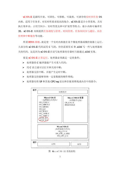
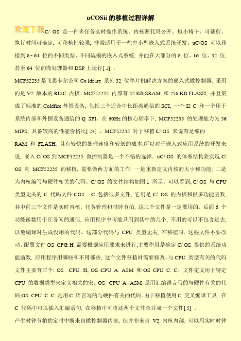
C/ OS 的文件结构如图1 所示。
可以看到, C/ OS 与CPU 类型无关的C 代码文件COS . C 包括很多文件, 它们是C/ OS 的内核和很多功能函数, 其中前三个文件是实时内核、任务管理和时钟节拍, 这三个文件是一定要用的。
后面6 个功能函数用于任务间的通信, 应用程序中可能只用到其中的几个, 不用的可以不包含进去, 以免编译时生成没用的代码。
这部分代码与CPU 类型无关, 在移植时, 这些文件不要改动。
配置文件OS_CFG. H 需要根据应用要求来进行,主要作用是确定C/ OS 提供的系统功能函数, 应用程序用哪些和不用哪些, 这个文件移植时需要修改。
©Freescale Semiconductor, Inc., 2006. All rights reserved.• PreliminaryFreescale SemiconductorData Sheet: Advance InformationMCF52235DS Rev. 0, 04/2006This document contains information on a new product. Specifications and information herein are subject to change without notice.Table of ContentsThe MCF52235 is a member of the ColdFire ® family of reduced instruction set computing (RISC)microprocessors. This hardware specification provides an overview of the 32-bit MCF52235 microcontroller,focusing on its highly integrated and diverse feature set. This 32-bit device is based on the Version 2 ColdFire core operating at a frequency up to 60 MHz, offering high performance and low power consumption. On-chip memories connected tightly to the processor core include 256 Kbytes of Flash and 32 Kbytes of static random access memory (SRAM). On-chip modules include:•V2 ColdFire core providing 56 Dhrystone 2.1 MIPS @ 60 MHz executing out of on-chip Flash memory using enhanced multiply accumulate (EMAC) and hardware divider.•Enhanced Multiply Accumulate Unit (EMAC) and hardware divide module•Cryptographic Acceleration Unit (CAU) coprocessor•Fast Ethernet Controller (FEC)•On-chip Ethernet Transceiver (ePHY)1MCF52235 Family Configurations.......................21.1Block Diagram ...................................................31.2Features.............................................................41.3Part Numbers and Packaging..........................161.4Package Pinouts..............................................171.5Reset Signals ..................................................241.6PLL and Clock Signals ....................................241.7Mode Selection................................................241.8External Interrupt Signals................................241.9Queued Serial Peripheral Interface (QSPI).....251.11I 2C I/O Signals.................................................271.12UART Module Signals .....................................271.13DMA Timer Signals..........................................271.16Pulse Width Modulator Signals........................281.17Debug Support Signals....................................281.18EzPort Signal Descriptions..............................301.19Power and Ground Pins...................................302Preliminary Electrical Characteristics. (313)Mechanical Outline Drawings (45)MCF52235 ColdFire® Microcontroller Data SheetSupports MCF52235, MCF52234, MCF52233, MCF52231, & MCF52230By: Microcontroller DivisionMCF52235 ColdFire® Microcontroller Data Sheet, Rev. 0PreliminaryMCF52235 Family ConfigurationsFreescale Semiconductor2•FlexCAN controller area network (CAN) module•Three universal asynchronous/synchronous receiver/transmitters (UARTs)•Inter-integrated circuit (I 2C™) bus controller •Queued serial peripheral interface (QSPI) module•Eight-channel 12-bit fast analog-to-digital converter (ADC)•Four channel direct memory access (DMA) controller•Four 32-bit input capture/output compare timers with DMA support (DTIM)•Four-channel general-purpose timer (GPT) capable of input capture/output compare, pulse width modulation (PWM) and pulse accumulation•Eight/Four-channel 8/16-bit pulse width modulation timers (two adjacent 8-bit PWMs can be concatenated to form a single 16-bit timer)•Two 16-bit periodic interrupt timers (PITs)•Real-time clock (RTC) module•Programmable software watchdog timer•Two interrupt controllers providing every peripheral with a unique selectable-priority interrupt vector plus seven external interrupts with fixed levels/priorities•Clock module with support for crystal or external oscillator and integrated phase locked loop (PLL)•Test access/debug port (JTAG, BDM)1MCF52235 Family ConfigurationsTable 1. MCF52235 Family ConfigurationsModule5223052231522335223452235ColdFire Version 2 Core with MAC (Multiply-Accumulate Unit)xxx xxSystem Clock60 MHz Performance (Dhrystone 2.1 MIPS)56Flash / Static RAM (SRAM)128/32 Kbytes256/32 KbytesInterrupt Controllers (INTC0/INTC1)x x x x x Fast Analog-to-Digital Converter (ADC)x x x x x Random Number Generator and Crypto Acceleration Unit (CAU)----x FlexCAN 2.0B Module-x -x x Fast Ethernet Controller (FEC) with on-chip interface (ePHY)x x x x x Four-channel Direct-Memory Access (DMA)xxxxxMCF52235 Family ConfigurationsMCF52235 ColdFire® Microcontroller Data Sheet, Rev. 0PreliminaryFreescale Semiconductor31.1Block DiagramThe MCF52235 (or its variants) come in 80- and 112-pin low-profile quad flat pack packages (LQFP) and a 121 MAPBGA, and operates in single-chip mode only. Figure 1 shows a top-level block diagram of the MCF52235.Software Watchdog Timer (WDT)x x x x x Programmable Interrupt Timer 22222Four-Channel General Purpose Timer x x x x x 32-bit DMA Timers 44444QSPI x x x x x UART(s)33333I 2Cx x x x x Eight/Four-channel 8/16-bit PWM Timer x x x x x General Purpose I/O Module (GPIO)x x x x x Chip Configuration and Reset Controller Modulex x x x x Background Debug Mode (BDM)x x x x x JTAG - IEEE 1149.1 T est Access Port 1x x x x x Package80-pin LQFP 112-pin LQFP80-pin LQFP 112-pin LQFP80-pin LQFP 112-pin LQFP80-pin LQFP 112-pin LQFP 121 MAPBGA112-pin LQFP 121 MAPBGANOTES:1The full debug/trace interface is available only on the 112- and 121-pin packages. A reduced debug interface is bonded on the 80-pin package.Table 1. MCF52235 Family Configurations (continued)Module5223052231522335223452235MCF52235 ColdFire® Microcontroller Data Sheet, Rev. 0PreliminaryMCF52235 Family ConfigurationsFreescale Semiconductor4Figure 1. MCF52235 Block Diagram1.2FeaturesThis document contains information on a new product under development. Freescale reserves the right to change or discontinue this product without notice. Specifications and information herein are subject to change without notice.ArbiterInterrupt Controller 1UART 0QSPIUART 1UART 2I 2CDTIM 0DTIM 1DTIM 2DTIM 3V2 ColdFire CPUIFPOEPEMAC4 CH DMA MUXJTAG TAPTo/From PADI32 Kbytes SRAM (4Kx16)x4256 Kbytes Flash (32Kx16)x4PORTS (GPIO)CIMRSTIN RSTOUTI 2C_SDA I 2C_SCL U n TXD U n RXD U n RTS DTIN n /DTOUT n CANRX JTAG_EN ADCAN[7:0]V RH V RLPLL CLKGENEdge Port 2FlexCAN EXTAL XTAL CLKOUTRNGA PIT1GPTPWMCANTX U n CTS PMMP A D I – P i n M u x i n gEzPortEzPCSQSPI_SCK,QSPI_PCS n PWM nQSPI_DIN,QSPI_DOUT ICOC n Fast EthernetController(FEC)EPHY EPHY_RX EPHY_TX PIT0Edge Port 1Interrupt Controller 2EzPQEzPD EzPCK RTCCAUMCF52235 Family ConfigurationsMCF52235 ColdFire® Microcontroller Data Sheet, Rev. 0PreliminaryFreescale Semiconductor51.2.1Feature Overview•Version 2 ColdFire variable-length RISC processor core —Static operation—32-bit address and data path on-chip —Up to 60MHz processor core frequency—Sixteen general-purpose 32-bit data and address registers—Implements ColdFire ISA_A+ with extensions to support the user stack pointer register, and 4new instructions for improved bit processing—Enhanced Multiply-Accumulate (EMAC) unit with four 48-bit accumulators to support 32-bit signal processing algorithms—Cryptography Acceleration Unit (CAU)–Tightly-coupled coprocessor to accelerate software-based encryption and message digest functions –FIPS-140 compliant random number generator–Support for DES, 3DES, AES, MD5, and SHA-1 algorithms —Illegal instruction decode that allows for 68K emulation support •System debug support—Real time trace for determining dynamic execution path —Background debug mode (BDM) for in-circuit debugging—Real time debug support, with four user-visible hardware breakpoint registers (PC and addresswith optional data) that can be configured into a 1- or 2-level trigger •On-chip memories—32 Kbyte dual-ported SRAM on CPU internal bus, accessible by core and non-core busmasters (e.g., DMA) with standby power supply support—256 Kbytes of interleaved Flash memory supporting 2-1-1-1 accesses •Power management—Fully static operation with processor sleep and whole chip stop modes—Very rapid response to interrupts from the low-power sleep mode (wake-up feature)—Software visible clock enable/disable for each peripheral •Fast Ethernet Controller (FEC)—10/100 BaseT/TX capability, half duplex or full duplex —On-chip transmit and receive FIFOs —Built-in dedicated DMA controller —Memory-based flexible descriptor ringsMCF52235 ColdFire® Microcontroller Data Sheet, Rev. 0Preliminary MCF52235 Family ConfigurationsFreescale Semiconductor6•On-chip Ethernet Transceiver (ePHY)—Digital adaptive equalization —Supports auto-negotiation —Baseline wander correction—Full-/Half-duplex support in all modes —Loopback modes—Supports MDIO preamble suppression —Jumbo packet•FlexCAN 2.0B Module—Based on and includes all existing features of the Freescale TOUCAN module —Full implementation of the CAN protocol specification version 2.0B –Standard Data and Remote Frames (up to 109 bits long)–Extended Data and Remote Frames (up to 127 bits long)–0-8 bytes data length–Programmable bit rate up to 1 Mbit/sec—Flexible Message Buffers (MBs), totalling up to 16 message buffers of 0–8 byte data length each, configurable as Rx or Tx, all supporting standard and extended messages —Unused Message Buffer space can be used as general purpose RAM space —Listen only mode capability —Content-related addressing—No read/write semaphores required—Three programmable mask registers: global (for MBs 0-13), special for MB14 and special forMB15—Programmable transmit-first scheme: lowest ID or lowest buffer number —“Time stamp” based on 16-bit free-running timer—Global network time, synchronized by a specific message —Programmable I/O modes —Maskable interrupts•Three Universal Asynchronous/synchronous Receiver Transmitters (UARTs)—16-bit divider for clock generation —Interrupt control logic —Maskable interrupts —DMA support—Data formats can be 5, 6, 7 or 8 bits with even, odd or no parity —Up to 2 stop bits in 1/16 increments —Error-detection capabilitiesMCF52235 Family ConfigurationsMCF52235 ColdFire® Microcontroller Data Sheet, Rev. 0PreliminaryFreescale Semiconductor7—Modem support includes request-to-send (URTS) and clear-to-send (UCTS) lines for twoUARTs—Transmit and receive FIFO buffers •I 2C Module—Interchip bus interface for EEPROMs, LCD controllers, A/D converters, and keypads —Fully compatible with industry-standard I 2C bus—Master or slave modes support multiple masters—Automatic interrupt generation with programmable level •Queued Serial Peripheral Interface (QSPI)—Full-duplex, three-wire synchronous transfers —Up to four chip selects available —Master mode operation only —Programmable master bit rates —Up to 16 pre-programmed transfers •Fast Analog-to-Digital Converter (ADC)—8 analog input channels —12-bit resolution—Minimum 2.25 µS conversion time—Simultaneous sampling of two channels for motor control applications —Single-scan or continuous operation—Optional interrupts on conversion complete, zero crossing (sign change), or under/over low/high limit—Unused analog channels can be used as digital I/O •Four 32-bit DMA Timers—16.7-ns resolution at 60 MHz—Programmable sources for clock input, including an external clock option —Programmable prescaler—Input-capture capability with programmable trigger edge on input pin —Output-compare with programmable mode for the output pin —Free run and restart modes—Maskable interrupts on input capture or reference-compare —DMA trigger capability on input capture or reference-compare •Four-channel general purpose timers —16-bit architecture—Programmable prescaler—Output pulse widths variable from microseconds to secondsMCF52235 ColdFire® Microcontroller Data Sheet, Rev. 0PreliminaryMCF52235 Family ConfigurationsFreescale Semiconductor8—Single 16-bit input pulse accumulator—Toggle-on-overflow feature for pulse-width modulator (PWM) generation —One dual-mode pulse accumulation channel •Pulse-width modulation timer—Operates as eight channels with 8-bit resolution or four channels with 16-bit resolution —Programmable period and duty cycle—Programmable enable/disable for each channel —Software selectable polarity for each channel—Period and duty cycle are double buffered. Change takes effect when the end of the current period is reached (PWM counter reaches zero) or when the channel is disabled. —Programmable center or left aligned outputs on individual channels—Four clock sources (A, B, SA, and SB) provide for a wide range of frequencies —Emergency shutdown•Two Periodic Interrupt Timers (PITs)—16-bit counter—Selectable as free running or count down •Real-Time Clock (RTC)—Maintains system time-of-day clock—Provides stopwatch and alarm interrupt functions •Software Watchdog Timer —32-bit counter—Low power mode support •Clock Generation Features —25 MHz crystal input—On-chip PLL can generate core frequencies up to maximum 60MHz operating frequency —Provides clock for integrated ePHY •Dual Interrupt Controllers (INTC0/INTC1)—Support for multiple interrupt sources organized as follows:–Fully-programmable interrupt sources for each peripheral –7 fixed-level interrupt sources –Seven external interrupt signals—Unique vector number for each interrupt source—Ability to mask any individual interrupt source or all interrupt sources (global mask-all)—Support for hardware and software interrupt acknowledge (IACK) cycles —Combinatorial path to provide wake-up from low power modesMCF52235 Family ConfigurationsMCF52235 ColdFire® Microcontroller Data Sheet, Rev. 0PreliminaryFreescale Semiconductor9•DMA Controller—Four fully programmable channels—Dual-address transfer support with 8-, 16- and 32-bit data capability along with support for 16-byte (4 X 32-bit) burst transfers—Source/destination address pointers that can increment or remain constant—24-bit byte transfer counter per channel—Auto-alignment transfers supported for efficient block movement —Bursting and cycle steal support—support for channel-to-channel linking—Software-programmable DMA channel selections in the UARTs (3) and 32-bit timers (4)•Reset—Separate reset in and reset out signals—Seven sources of reset:–Power-on reset (POR)–External –Software –Watchdog –Loss of clock –Loss of lock–Low-voltage detection (LVD)—Status flag indication of source of last reset •Chip Integration Module (CIM)—System configuration during reset —Selects one of six clock modes—Configures output pad drive strength—Unique part identification number and part revision number •General Purpose I/O interface—Up to 73 bits of general purpose I/O—Bit manipulation supported via set/clear functions —Unused peripheral pins may be used as extra GPIO •JTAG support for system level board testing1.2.2V2 Core OverviewThe Version 2 ColdFire processor core is comprised of two separate pipelines that are decoupled by an instruction buffer. The two-stage Instruction Fetch Pipeline (IFP) is responsible for instruction-address generation and instruction fetch. The instruction buffer is a first-in-first-out (FIFO) buffer that holdsMCF52235 ColdFire® Microcontroller Data Sheet, Rev. 0PreliminaryMCF52235 Family ConfigurationsFreescale Semiconductor10prefetched instructions awaiting execution in the Operand Execution Pipeline (OEP). The OEP includes two pipeline stages. The first stage decodes instructions and selects operands (DSOC); the second stage (AGEX) performs instruction execution and calculates operand effective addresses, if needed.The V2 core implements the ColdFire Instruction Set Architecture Revision A+ (see the ColdFire Family Programmer’s Reference Manual for instruction set details) which includes support for a separate user stack pointer register and four new instructions to assist in bit processing. Additionally, the MCF52235core includes the enhanced multiply-accumulate unit (EMAC) for improved signal processing capabilities.The MAC implements a 4-stage arithmetic pipeline, optimized for 32 x 32 bit operations, with support for four 48-bit accumulators. Supported operands include 16- and 32-bit signed and unsigned integers as well as signed fractional operands and a complete set of instructions to process these data types. The EMAC provides superb support for execution of DSP operations within the context of a single processor at a minimal hardware cost.1.2.3Debug ModuleThe ColdFire processor core debug interface is provided to support system debugging in conjunction with low-cost debug and emulator development tools. Through a standard debug interface users can access debug information, and on 112- and 121-lead packages real-time tracing capability is provided. This allows the processor and system to be debugged at full speed without the need for costly in-circuit emulators. The debug interface is a superset of the BDM interface provided on Freescale’s 683xx family of parts. The MCF52235 supports Revision B+ of the ColdFire debug architecture (DEBUG_B+).The on-chip breakpoint resources include a total of nine programmable 32-bit registers: two address registers, two data registers (one data register and one data mask register), four 32-bit PC registers and one PC mask register. These registers can be accessed through the dedicated debug serial communication channel or from the processor’s supervisor mode programming model. The breakpoint registers can be configured to generate triggers by combining the address, data, and PC conditions in a variety of single-or dual-level definitions. The trigger event can be programmed to generate a processor halt or initiate a debug interrupt exception.The MCF52235’s interrupt servicing options during emulator mode allow real-time critical interrupt service routines to be serviced while processing a debug interrupt event, thereby ensuring that the system continues to operate even during debugging.To support program trace, the V2 debug module provides processor status (PST[3:0]) and debug data (DDATA[3:0]) ports. These buses and the PSTCLK output provide execution status, captured operand data, and branch target addresses defining processor activity at the CPU’s clock rate. The MCF52235includes a new debug signal, ALLPST. This signal is the logical ‘AND’ of the processor status (PST[3:0])signals and is useful for detecting when the processor is in a halted state (PST[3:0] = 1111).The full debug/trace interface is available only on the 112- and 121-pin packages. However, every product features the dedicated debug serial communication channel (DSI, DSO, DSCLK) and the ALLPST signal.1.2.4JTAGThe MCF52235 supports circuit board test strategies based on the Test Technology Committee of IEEE and the Joint Test Action Group (JTAG). The test logic includes a test access port (TAP) consisting of aMCF52235 Family ConfigurationsMCF52235 ColdFire® Microcontroller Data Sheet, Rev. 0PreliminaryFreescale Semiconductor1116-state controller, an instruction register, and three test registers (a 1-bit bypass register, a 256-bit boundary-scan register, and a 32-bit ID register). The boundary scan register links the device’s pins into one shift register. Test logic, implemented using static logic design, is independent of the device system logic.The MCF52235 implementation can do the following:•Perform boundary-scan operations to test circuit board electrical continuity•Sample MCF52235 system pins during operation and transparently shift out the result in the boundary scan register•Bypass the MCF52235 for a given circuit board test by effectively reducing the boundary-scan register to a single bit•Disable the output drive to pins during circuit-board testing •Drive output pins to stable levels1.2.5On-Chip Memories1.2.5.1SRAMThe SRAM module provides a general-purpose 32-Kbyte memory block that the ColdFire core can access in a single cycle. The location of the memory block can be set to any 32-Kbyte boundary within the 4-Gbyte address space. This memory is ideal for storing critical code or data structures and for use as the system stack. Because the SRAM module is physically connected to the processor's high-speed local bus,it can quickly service core-initiated accesses or memory-referencing commands from the debug module.The SRAM module is also accessible by the DMA. The dual-ported nature of the SRAM makes it ideal for implementing applications with double-buffer schemes, where the processor and a DMA device operate in alternate regions of the SRAM to maximize system performance.1.2.5.2FlashThe ColdFire Flash Module (CFM) is a non-volatile memory (NVM) module that connects to the processor’s high-speed local bus. The CFM is constructed with four banks of 32K x 16-bit Flash arrays to generate 256 Kbytes of 32-bit Flash memory. These arrays serve as electrically erasable and programmable, non-volatile program and data memory. The Flash memory is ideal for program and data storage for single-chip applications, allowing for field reprogramming without requiring an external high voltage source. The CFM interfaces to the ColdFire core through an optimized read-only memory controller which supports address speculation and interleaved accesses from the 2-cycle Flash arrays for improved performance. For operation at reduced core frequencies, the access time can be decreased (under program control) to a single-cycle access. A backdoor mapping of the Flash memory is used for all program, erase, and verify operations, as well as providing a read datapath for the DMA. Flash memory may also be programmed via the EzPort, which is a serial Flash programming interface that allows the Flash to be read, erased and programmed by an external controller in a format compatible with most SPI bus Flash memory chips. This allows easy device programming via Automated Test Equipment or bulk programming tools.MCF52235 ColdFire® Microcontroller Data Sheet, Rev. 0PreliminaryMCF52235 Family ConfigurationsFreescale Semiconductor121.2.6Power ManagementThe MCF52235 incorporates several low power modes of operation which are entered under program control and exited by several external trigger events. An integrated power-on reset (POR) circuit monitors the input supply and forces an MCU reset as the supply voltage rises. The low voltage detector (LVD)monitors the supply voltage and is configurable to force a reset or interrupt condition if it falls below the LVD trip point.1.2.7Fast Ethernet Controller (FEC)The integrated Fast Ethernet Controller (FEC) performs the full set of IEEE ® 802.3/Ethernet CSMA/CD media access control and channel interface functions. The FEC connects through the on-chip transceiver (ePHY) which provides the physical layer interface.1.2.8Ethernet Physical Interface (ePHY)The ePHY is an IEEE 802.3 compliant 10/100 Ethernet physical transceiver. The ePHY can be configured to support 10BASE-T or 100BASE-TX applications. The ePHY is configurable via internal registers.There are five basic modes of operation for the ePHY:•Power down/initialization •Auto-negotiate •10BASE-T •100BASE-TX •Low-power1.2.9Cryptography Acceleration UnitThe MCF52235 device incorporates two hardware accelerators for cryptographic functions. First, the CAU is a coprocessor tightly-coupled to the V2 ColdFire core that implements a set of specialized operations to increase the throughput of software-based encryption and message digest functions,specifically the DES, 3DES, AES, MD5 and SHA-1 algorithms. Second, a random number generator provides FIPS-140 compliant 32-bit values to security processing routines. Both modules supply critical acceleration to software-based cryptographic algorithms at a minimal hardware cost.1.2.10FlexCANThe FlexCAN module is a communication controller implementing version 2.0 of the CAN protocol parts A and B. The CAN protocol can be used as an industrial control serial data bus, meeting the specific requirements of reliable operation in a harsh EMI environment with high bandwidth. This instantiation of FlexCAN has 16 message buffers.MCF52235 Family ConfigurationsMCF52235 ColdFire® Microcontroller Data Sheet, Rev. 0PreliminaryFreescale Semiconductor131.2.11UARTsThe MCF52235 has three full-duplex UARTs that function independently. The three UARTs can be clocked by the system bus clock, eliminating the need for an external clock source. On smaller packages,the third UART is multiplexed with other digital I/O functions.1.2.12I 2C BusThe I 2C bus is a two-wire, bidirectional serial bus that provides a simple, efficient method of data exchange and minimizes the interconnection between devices. This bus is suitable for applications requiring occasional communications over a short distance between many devices on a circuit board.1.2.13QSPIThe queued serial peripheral interface (QSPI) provides a synchronous serial peripheral interface with queued transfer capability. It allows up to 16 transfers to be queued at once, minimizing the need for CPU intervention between transfers.1.2.14ADCThe Fast ADC consists of an eight-channel input select multiplexer and two independent sample and hold (S/H) circuits feeding separate 12-bit ADCs. The two separate converters store their results in accessible buffers for further processing.The ADC can be configured to perform a single scan and halt, perform a scan whenever triggered, or perform a programmed scan sequence repeatedly until manually stopped.The ADC can be configured for either sequential or simultaneous conversion. When configured for sequential conversions, up to eight channels can be sampled and stored in any order specified by the channel list register. Both ADCs may be required during a scan, depending on the inputs to be sampled.During a simultaneous conversion, both S/H circuits are used to capture two different channels at the same time. This configuration requires that a single channel may not be sampled by both S/H circuits simultaneously.Optional interrupts can be generated at the end of the scan sequence if a channel is out of range (measures below the low threshold limit or above the high threshold limit set in the limit registers) or at several different zero crossing conditions.1.2.15DMA Timers (DTIM0–DTIM3)There are four independent, DMA transfer capable 32-bit timers (DTIM0, DTIM1, DTIM2, and DTIM3)on the MCF52235. Each module incorporates a 32-bit timer with a separate register set for configuration and control. The timers can be configured to operate from the system clock or from an external clock source using one of the DTINx signals. If the system clock is selected, it can be divided by 16 or 1. The input clock is further divided by a user-programmable 8-bit prescaler which clocks the actual timer counter register (TCRn). Each of these timers can be configured for input capture or reference (output) compare mode. Timer events may optionally cause interrupt requests or DMA transfers.MCF52235 ColdFire® Microcontroller Data Sheet, Rev. 0PreliminaryMCF52235 Family ConfigurationsFreescale Semiconductor141.2.16General Purpose Timer (GPT)The general purpose timer (GPT) is a four-channel timer module consisting of a 16-bit programmable counter driven by a 7-stage programmable prescaler. Each of the four channels can be configured for input capture or output compare. Additionally, one of the channels, channel 3, can be configured as a pulse accumulator.A timer overflow function allows software to extend the timing capability of the system beyond the 16-bit range of the counter. The input capture and output compare functions allow simultaneous input waveform measurements and output waveform generation. The input capture function can capture the time of a selected transition edge. The output compare function can generate output waveforms and timer software delays. The 16-bit pulse accumulator can operate as a simple event counter or a gated time accumulator.1.2.17Periodic Interrupt Timers (PIT0 and PIT1)The two periodic interrupt timers (PIT0 and PIT1) are 16-bit timers that provide interrupts at regular intervals with minimal processor intervention. Each timer can either count down from the value written in its PIT modulus register, or it can be a free-running down-counter.1.2.18Pulse Width Modulation TimersThe MCF52235 has an 8-channel, 8-bit PWM timer. Each channel has a programmable period and duty cycle as well as a dedicated counter. Each of the modulators can create independent continuous waveforms with software-selectable duty rates from 0% to 100%. The PWM outputs have programmable polarity, and can be programmed as left aligned outputs or center aligned outputs. For higher period and duty cycle resolution, each pair of adjacent channels ([7:6], [5:4], [3:2], and [1:0]) can be concatenated to form a single 16-bit channel. The module can thus be configured to support 8/0, 6/1, 4/2, 2/3, or 0/4 8-/16-bit channels.1.2.19Real-Time Clock (RTC)The Real-Time Clock (RTC) module maintains the system (time-of-day) clock and provides stopwatch,alarm, and interrupt functions. It includes full clock features: seconds, minutes, hours, days and supports a host of time-of-day interrupt functions along with an alarm interrupt.1.2.20Software Watchdog TimerThe watchdog timer is a 16-bit timer that facilitates recovery from runaway code. The watchdog counter is a free-running down-counter that generates a reset on underflow. To prevent a reset, software must periodically restart the countdown.1.2.21Phase Locked Loop (PLL)The clock module supports an external crystal oscillator and includes a phase-locked loop (PLL), reduced frequency divider (RFD), low-power divider status/control registers, and control logic. In order to improve。
这是freescale的coldfire V2系列的一款32位微处理器,使用心得颇多,略记点点。
1、基本配置MCF52233 CPU, 112 pins? 256 Byte Flash? 32K Byte Ram //比起经常使用的单片机,超级爽? DMA Controller w/ Timers? Programmable Interrupt Timer? 8ch, 12b ADC? QSPI, IIC, and CAN Serial Ports? Fast Ethernet Controller (FEC) and EthernetPhy (ePHY)? 3 x UART Serial Ports with DMA capability? 4 GPT Timers? BDM / JTAG Port? 3.3V operation? 60 MHz Internal Bus //速度相当快? 40 pin I/O port? Ethernet port? Integrated USB BDM port? BDM / JTAG Port (not installed)2、使用调试编译软件codewarrior,建立一个新项目后,support files文件夹中自动如下文件:mcf52233_vectors.s(向量表配置文件)、mcf5xxx_lo.s、mcf52233_lo.s(启动代码)等等。
在mcf52233_vectors.s文件中,move.w #0x2700,srjmp _asm_startmeup.end此条语句必须改为move.w #0x2000,sr 才能使用所有中断,初学者常常会忽略此点。
3、启动代码中if (__VECTOR_RAM != VECTOR_TABLE){for (n = 0; n < 256; n++)__VECTOR_RAM[n] = VECTOR_TABLE[n];}mcf5xxx_wr_vbr((uint32)__VECTOR_RAM);VECTOR_TABLE在mcf52235_vectors.s里定义,为中断向量表,保存着各个中断服务函数的地址,长度为256 x 4字节。
UCOS-II的详细移植笔记两种处理器的移植比较(S1C33209S3C44BOX)UC/OS-II的详细移植笔记两种处理器的移植比较(S1C33209&&S3C44BOX) [原创 2007-05-20 23:03:21] 字号:大中小UC/OS-II的移植步骤分析zqcumt 07-4-15关于UC/OS-II的移植网上介绍的已经很多了,比较流行的几款处理器(例如ARM)在网上都可以直接下载移植好的代码。
由于最近选修了一门嵌入式系统的课,用的处理器是EPSON公司的S1C33系列,做实验的时候要进行操作系统的移植,这个周末花了一天半的时间学习了一下,因为毕业设计的时候做过ARM上的移植,于是将两者比较了一下,给出一般的移植要点。
由于将来实验还要设计到GUI的移植以及文件系统的移植和网络协议的移植,我会将自己的学习笔记都记录下来。
大家下载到源码后,针对Intel 80x86的代码在uCOS-II\Ix86L目录下。
代码是80x86实模式,且在编译器大模式下编译的。
移植部分的代码可在下述文件中找到:OS_CPU.H, OS_CPU_C.C, 和OS_CPU_A.ASM。
大家可以参考这个例子,对它进行修改。
INCLUDES.H 是主头文件,在所有后缀名为.C的文件的开始都包含INCLUDES.H文件。
使用INCLUDES.H的好处是所有的.C文件都只包含一个头文件,程序简洁,可读性强。
缺点是.C文件可能会包含一些它并不需要的头文件,额外的增加编译时间。
与优点相比,多一些编译时间还是可以接受的。
用户可以改写INCLUDES.H文件,增加自己的头文件,但必须加在文件末尾。
/////////////////////////////////////////////////////////////////// ////////////一、(1)OS_CPU.H文件的移植 (针对S1C33209)//////////////////////////////////////////////////////////////////////////OS_CPU.H 文件中包含与处理器相关的常量,宏和结构体的定义。
L C /OS -Ò在Coldfire MCF52235上的移植孙庆轩,孙同景,陶 亮(山东大学控制科学与工程学院 山东济南 250061)摘 要:介绍将L C/OS -Ò实时操作系统移植到Co ldfire 处理器M CF 52235上的方法,为M CF5223x 系列微控制器的软件开发提供了一个实时操作系统平台。
首先分析L C/OS -Ò的特点和内核结构,结合M CF52235的结构特点以及使用的软硬件开发工具,深入研究移植条件和实现方法,详细阐述系统移植中需要修改的文件、编写的代码及需要注意的问题。
然后使用Co dew arr ior 6.4集成开发环境和评估板,通过建立两个应用任务,验证了移植代码的正确性,说明在M CF52235上移植L C/OS -Ò是成功和可行的。
在此介绍的移植过程和方法可以作为L C/O S -Ò在其他微控制器中移植的典型范例。
关键词:L C/O S -Ò;移植;Co ldfir e;M CF52235中图分类号:T P311 文献标识码:A 文章编号:1004-373X(2010)06-029-05Transplantation of L C/OS -Òon C oldfire MCF52235SU N Q ingx uan,SU N T ongjing,T A O L iang(Schoo l of Co nt rol Science and Eng i neeri ng,Sha ndong U ni v ersity ,Ji c nan,250061,Chi na)Abstract :T r ansplanting L C/OS -II to Coldfire M CF52235,a r ea-l time operating system platfor m is prov ided fo r softw are development upon micro contro ller M CF 5223x.T he cha racteristics and ker nel str uctur e of L C/O S -I I ar e analyzed.Conditio ns and implemenatio n o f transplant at ion accor ding t o t he st ruct ur e of M CF52235and softw are/har dw are dev elopment to ols are deeply researched,the files and the code need t o be mo dified and the pr oblems sho uld be noticed are illuminated.T he co rr ect -ness of por ted codes is v alidated by establishing two application tasks on ev aluatio n board by Codewar rior 6.4IDE.T he results sho w that the tansplantat ion of L C/OS -II o n Coldfire M CF 52235is successful and feasible.T he pro cess and implement ation of transplant ation shall be a ty pica l ex am ple for t ansplantatio n o f L C/OS -Òto other microcontr ollers.Keywords :L C/OS -II ;tansplantat ion;Co ldfire;M CF52235收稿日期:2009-10-280 引 言L C/OS -Ò是一种多任务实时操作系统。
内核源代码公开、短小精干、可裁剪、执行时间可确定,可移植性较强,非常适用于一些中小型嵌入式系统开发。
L C/OS -Ò可以移植到8~64位的不同类型、不同规模的嵌入式系统,并能在大部分的8位、16位、32位,甚至64位的微处理器和DSP 上运行[1]。
MCF52235是飞思卡尔公司Co ldfire 系列32位单片机解决方案的嵌入式微控制器,采用的是V2版本的RISC 内核。
M CF52235内部有32KB SRAM 和256KB FLASH ,并且集成了标准的Coldfire 外围设备,包括三个适合中长距离通信的SCI,一个I 2C 和一个用于系统内部和外围设备通信的Q SPI 。
在60H z 的核心频率下,MCF52235的处理能力为56M IPS,具备较高的性能价格比[2-4]。
MCF52235对于移植L C/OS -Ò来说有足够的RAM 和FLASH ,且有较快的处理速度和较低的成本,所以对于嵌入式应用系统的开发来说,嵌入L C/OS -Ò到M CF52235微控制器是一个不错的选择。
1 L C /OS -Ò的体系结构要实现L C/OS -Ò向M CF52235的移植,需要做两方面的工作:一是重新定义内核的大小和功能;二是为内核编写与硬件相关的代码。
L C/OS -Ò的文件结构如图1所示。
可以看到,L C/OS -Ò与CPU 类型无关的C 代码文件L COS -Ò.C 包括很多文件,它们是L C/OS -Ò的内核和很多功能函数,其中前三个文件是实时内核、任务管理和时钟节拍,这三个文件是一定要用的。
后面6个功能函数用于任务间的通信,应用程序中可能只用到其中的几个,不用的可以不包含进去,以免编译时生成没用的代码。
这部分代码与CPU 类型无关,在移植时,这些文件不要改动。
配置文件OS_CFG.H 需要根据应用要求来进行,主要作用是确定L C/OS -Ò提供的系统功能函数,应用29程序用哪些和不用哪些,这个文件移植时需要修改。
与CPU 类型有关的代码文件主要有三个:OS _CPU.H ,OS_CPU_A.ASM 和OS_CPU_C.C 。
文件定义用于特定CPU 的数据类型来定义相关的宏。
OS _CPU_A.ASM 是用汇编语言写的与硬件有关的代码,OS_CPU_C.C 是用C 语言写的与硬件有关的代码。
由于移植使用C 交叉编译工具,在C 代码中可以插入汇编语句,在移植中可将这两个文件合并成一个文件[5]。
产生时钟节拍的定时中断来自微控制器内部,但并非来自V2内核内部,可以用实时时钟产生定时中断,也可以用片内的外设模块定时器单元来产生定时中断,这部分代码显然与硬件相关,移植时要自己写[6]。
图1 L C/O S -Ò的文件结构2 移植过程所谓移植,就是使一个实时内核能在某个微处理器或微控制器上运行。
为了方便移植,大部分的L C/OS -Ò代码是用C 语言写的,但仍需要用C 和汇编语言写一些与处理器相关的代码,这是因为L C/OS -II 在读写处理器寄存器时只能通过汇编语言来实现[7]。
移植过程主要包括移植前的准备、BSP (板级支持包)的编写和与处理器相关代码的修改和编写。
L C/OS -Ò核心代码、与CPU 相关的接口程序、BSP 和用户应用程序之间的关系如图2所示。
2.1 移植前的准备进入L C/OS -Ò官方网站下载L C/OS -Ò源代码。
打开Codew arrior 6.4建立M CF52235的工程文件,然后把L C/OS -Ò的源代码文件加入到工程里面[8]。
其中有几个地方需要改动:(1)下载的源代码中os_cfg _r.h 改为o s_cfg.h;os_dbg_r.c 改为os_dbg.c 。
(2)由于会引起重复定义错误,需要把源代码中重复包含的文件注释掉。
(3)需要在INT ERNAL_FLASH 模式下编译,而不能在RAM 模式下,否则会产生溢出错误。
图2 系统中各部分之间的关系2.2 编写BSP板级支持包(BSP)是介于底层硬件和操作系统之间的软件层次,负责进行系统启动后最初的硬件和软件初始化,并对底层硬件进行封装,使得操作系统不再面对具体的硬件[9]。
在此建立两个BSP 文件:BSP.ASM 和BSP.C 。
其中,BSP.ASM 中包含了汇编语言写的中断接口程序。
BSP.C 中包含了硬件和软件的初始化程序和产生时钟节拍的中断服务程序。
2.3 与处理器相关代码的修改和编写有三个与处理器相关的文件,即OS_CPU.H ,OS_CPU _A.ASM 和OS _CPU _C.C 需要修改。
由于M CF52235有eM AC 模块,所以还需要编写OS_CPU _I.ASM 文件,用来在任务切换和中断时以及中断返回时保存和恢复相关寄存器。
2.3.1 OS_CPU.H 的移植OS_CPU.H 包含了一些与处理器和编译器相关的宏定义和数据类型定义。
由于使用Codew arrior 编译器,shor t 类型是16位的,int 类型是32位的。
M CF52235的堆栈是32位宽的,因此OS_STK 定义为32位,所有任务的堆栈必须声明使用OS_ST K 这种数据类型。
数据类型定义如下:ty pedef unsigned char BOO L EAN ;ty pedef unsigned char INT 8U ;ty pedef signed char IN T 8S;ty pedef unsigned sho rt IN T 16U ;ty pedef signed shor t IN T 16S;ty pedef unsigned int IN T 32U ;ty pedefsigned int I NT 32S;30typedef float F P32;typedef double FP64;typedef unsigned int O S_ST K;typedef unsigned shor t OS_CP U_SR;(1)临界区域处理。
像所有的实时性内核一样,在进入代码临界区时要关中断,完成时要开中断。
L C/ OS-Ò定义了两个宏来关闭和使能中断:OS_ENT ER_ CRITICAL()和OS_EXIT_CRIT ICAL()。
L C/OS-Ò定义了三种方法来关闭和使能中断,大多数情况下选择第三种方法。