Zigbee模块选型手册
- 格式:pdf
- 大小:905.51 KB
- 文档页数:8
XBee和XBee-PRO OEM RF模块的设计,以ZigBee协议内运作,支持低成本的独特需求,低功耗无线传感器网络工程。
模块只需要最小的功率,就能提供远程设备之间的数据传输的可靠性。
这两个模块内运作的ISM2.4GHz频段,且引脚对引脚相互兼容。
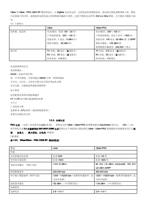
1.1主要特点XBee XBee-PRO高性能、低成本室内/城市:距离100'(30米)户外线的视线:300'(100米)发射功率:1毫瓦(0dBm时)接收灵敏度:-92dBm的室内/城市:300'(100米)户外线的视线:高达1英里(1500米)发射功率:100毫瓦(20dBm的)的EIRP 接收灵敏度:-100dBm的射频数据传输速率:250,000个基点低功率TX电流:45毫安(@3.3伏)RX电流:50毫安(@3.3伏)掉电电流:<10微安TX电流:215毫安(@3.3伏)RX电流:55毫安(@3.3伏)掉电电流:<10微安先进的网络和安全重试和确认。
DSSS(直接序列扩频)每一个序列频道,可使用超过65000个唯一的网络地址点至点,点对点,点对多点和点对点的对等拓扑支撑自行安排,自我修复和故障容错网络易于使用没有配置必要的外箱射频通信AT和API命令模式配置模块参数小尺寸广泛的命令集免费的X-CTU软件(测试和配置软件)免费及无限技术支持1.1.1.全球认证FCC认证(美国)参见附录A[p34要求]。
系统包含的XBee/XBee-PRO射频模块继承MaxStream的认证。
ISM(工业,科学和医疗)2.4吉赫频带的ISO9001:2000认证机构认证下制造的注册标准的XBee/XBee-PRO射频模块列表被优化用于在美国,加拿大,澳大利亚,以色列和欧洲。
1.2.描述表1-01,XBee/XBee‐PRO OEM RF模块(简述)描述xbee XBee-PRO性能室内和城市的范围距离30M距离100米室外的可视范围距离100m距离1500米发射功率输出(软件可选)1mW(0dBm)60mW(18dBm)conducted,100mW(20dBm)EIRP*射频数据速率250,000bps250,000bps串行接口数据速率(软件可选)1200-115200bps(标准的传输速率,也支持非标准)1200-115200bps(标准的传输速率,也支持非标准)接收器灵敏度-92dBm(1%的错误包)-100dBm(1%的错误包)电源要求电源电压 2.8–3.4V 2.8–3.4V工作电流(发送)45mA(@3.3V)If PL=0(10dBm):137mA(@3.3V),139mA(@3.0V)PL=1(12dBm):155mA(@3.3V),153mA(@3.0V)PL=2(14dBm):170mA(@3.3V),171mA(@3.0V)PL=3(16dBm):188mA(@3.3V),195mA(@3.0V)PL=4(18dBm):215mA(@3.3V),227mA(@3.0V)工作电流(接收)50mA(@3.3V)55mA(@3.3V)掉电电流不支持不支持概要操作频段ISM2.4GHz ISM2.4GHz尺寸0.960”x1.087”(2.438cm x2.761cm)0.960”x1.297”(2.438cm x3.294cm)工作温度-40to85o C(industrial)-40to85o C(industrial)天线选择集成带,芯片或U.FL连接器集成带,芯片或U.FL连接器网络与安全支持的网络拓扑点至点,点对多点,对等网络与网孔通道数量(软件可选)16个直接序列通道16个直接序列通道寻址选项PAN编号,通道和地址PAN编号,通道和地址机构认证美国(FCC15.247部分)OUR-XBEE OUR-XBEEPRO加拿大工业部(IC)4214A XBEE4214A XBEEPRO欧盟ce ETSI ETSI(Max.10dBm transmit poweroutput)*当在欧洲运用时:XBee-PRO RF模块必须被配置为运行在一个最大发射功率为10dBm的输出水平。
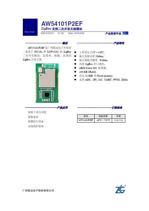
——————————————概述AW54101P2EF 是广州致远电子开发的一款基于JN5161和LCP54101的ZigBee 二次开发模块,是简单、快捷、高效的ZigBee 开发方案。
————————————产品应用家庭工业自动化 智能家居 便携医疗设备 无线监控系统广州致远电子股份有限公司修订历史目录1. 产品简介 (1)1.1产品概述 (1)1.2产品特征 (1)1.3模块尺寸 (1)1.4命名规则 (2)1.5产品选型表 (2)2. 硬件描述 (3)2.1引脚分布 (3)2.2全引脚说明 (3)3. 电气特性 (10)3.1LPC54101管脚电气特性 (10)3.2功耗特性 (10)3.3RF特性 (11)4. 典型应用 (12)4.1应用电路 (12)4.2板载天线布局注意事项 (13)4.3外接天线布局注意事项 (13)5. 机械尺寸 (14)6. 免责声明 (15)1. 产品简介1.1 产品概述AW54101P2EF 无线开发模块是广州致远电子股份有限公司基于NXP 的JN5161、LPC54101芯片开发的低功耗、高性能型ZigBee 二次开发模块。
其中LPC54101是采用ARM@CortexTM-M4内核的32位低功耗处理器,主频高达100Mhz ,支持512KB 片内Flash 存储器和104KB 片内SRAM 存储器。
该处理器集成了灵活的外设模块,支持I2C 、UART 、SPI 、ADC 、TIMER 、PWM 等功能。
而JN5161是NXP 的ZigBee 芯片,提供了一个完整的基于IEEE802.15.4标准ISM (2.4-2.5GHz )频段的应用集成方案,支持FastZigBee 协议。
集合这两款芯片的优势,AW54101P2EF 无线开发模块可快速应用于工业控制、工业数据采集、农业控制、矿区人员定位、智能家居,智能遥控器等场合,大幅减小开发难度,使用户产品更快的投入市场,增加用户产品的竞争力,更好的把握住先机。
The XBee family of ZigBee/802.15.4 RF modules is the premiere choice for OEMs looking for excellent wireless performance in a cost-effective, small form factor solution. Each XBee module comes in either a regular or long-range “–PRO” version*. All XBee modules are pin-for-pin compatible with the exception of a few varying I/O features, which provides a standard footprint for OEMs with multiple applications.XBee Series 1 is based on ZigBee/802.15.4 silicon from Freescale ®. Its 802.15.4 firmware feature set makes it ideal for point-to-point, peer-to-peer, and point-to-multipoint (star) topologies. The XBee Series 1 gives the user maximum control over network nodes and minimum latency. XBee Series 2 is based on ZigBee/802.15.4 silicon from Ember™. It features ZigBee firmware for creating ad-hoc mesh networks. The XBee Series 2 performs automatic route discoveries to create a self-healing network of full-function routers and low-power end devices. XBee Series 1and Series 2 modules do not communicate with one another.Known for ease of use, the XBee modules are ready to operate out of the box and offer simple AT commands or an API for advanced, user-settable configurations. XBee modules arerecognized worldwide for reliable wireless data communication in the license-free 2.4 GHz ISM band. Visit our website for a complete listing of countries that have approved the XBee as a certified, license-free RF module with no need for further testing.XBee modules are a part of Digi’s full line of Drop-in Networking products. ConnectPort X gateways and XBee device adapters, modules and extenders provide end-to-end wirelessconnectivity to commercial-grade electronic devices in locations where wired infrastructure does not exist or satisfy customer needs. To learn more about Drop-in Networking, visit /products/wirelessdropinnetworking.Part of Digi’s Drop-in Networking product family,XBee OEM RF modules provide reliable, wireless data communication over ZigBee/802.15.4 networks.Available in Series 1 or Series 2 models for point-to-multipoint or mesh topologies, they enable OEMs with excellent wireless performance in a cost-effective,small form factor solution.Features/Benefits•ZigBee/802.15.4 compatible RF modules • 2.4 GHz ISM band for use worldwide •Fully interoperable with other Digi Drop-in Networkingproducts, including gateways, device adapters and extenders •Available in Series 1 or Series 2 models for point-to-multipoint or mesh topologies •Pin-swappable regular and long-range –PRO versions •Low cost•Common footprint for a variety of Digi RF modules •Low-power sleep modes •Multiple antenna options •Industrial temperature (-40º C to 85º C)Central Facilities ManagementEthernetConnectPort ™ XGatewayGa a te wa w y Wireless Telco NetworkWarehouseInternet/Frame Relay/VPNMeterMeterMeterXBee ™ModuleZigBee/802.15.4Wireless Mesh Network2.4 GHz OEM RF ModulesProduct DatasheetOverviewXBee ™ZigBee®/802.15.4 ModulesSeries 1•Serial data rate:1200 - 250000 bps •(6) 10-bit ADC inputs,(8) Digital I/O Series 2•Serial data rate: 1200 – 1 Mbps •(4) 10-bit ADC inputs,(10) Digital I/O91001412A1/1007© 2006-2007 Digi International Inc.All rights reserved. Digi, Digi International, the Digi logo, the When Reliability Matters logo, ConnectPort, XBee, XBee-PRO and XStream are either trademarks or registered trademarks of Digi International Inc. in the United States and other countries worldwide. All other trademarks are the property of their respective holders.Digi Internationa l11001 Bren Road E.Minnetonka, MN 55343U.S.A.PH:877-912-3444952-912-3444FX:952-912-4952email:*************Digi Internationa l France31 rue des Poissonniers 92200 Neuilly sur Seine PH: +33-1-55-61-98-98 FX: +33-1-55-61-98-99www.digi.frDigi Internationa l KKNES Building South 8F 22-14 Sakuragaoka-cho,Shibuya-kuTokyo 150-0031, Japan PH: +81-3-5428-0261FX: +81-3-5428-0262www.digi-intl.co.jpDigi Internationa l (HK) LimitedSuite 1703-05, 17/F .,K Wah Centre 191 Java RoadNorth Point, Hong Kong PH:+852-2833-1008FX: +DIGI SERVICE AND SUPPORT - You can purchase with confidence knowing that Digi is hereto support you with expert technical support and a one-year warranty. /supportDigi International , the leader in device networking for business, develops reliable products and technologies to connect and securely manage local or remote electronic devices over the network or via the web. With over 20 million ports shipped worldwide since 1985, Digi offers the highest levels of performance, flexibility and quality.4214A-XBEEPRO•Europe (CE): ETSI / ETSI(max. tx power output: 10 mW)•Australia •JapanSeries 2 (XBee)•U.S. (FCC Part 15.247): OUR-XBEE2 •Canada (IC): 4214A-XBEE2•Europe (CE): ETSI •JapanPlease visit for part numbers.•Encryption: AES 128-bit •Reliable packet delivery: Retries/Acknowledgments •PAN ID, 64-bit IEEE MAC address, 16 channels(12 channels – XBee-PRO Series 1)N E T W O R K I N G A N D S E C U R I T Y1.087”(2.761)0.960”(2.438)•Transmit power output: 1 mW (0 dBm) / 60 mW (+18 dBm) -Note:In Europe XBeePRO modules must be set to 10 mW (10 dBm). In Japan XBP modules are calibrated to 10 mW (10 dBm).•Receiver sensitivity (1% PER):-92 dBm / -100 dBm Series 2 (XBee)•Indoor/Urban range: 133 ft (40 m)•Outdoor/RF line-of-sight range: 400 ft (120 m)•Transmit power output:1.25 mW (+1 dBm) (2 mW (+3 dBm) boost mode)•Receiver sensitivity (1% PER):-97 dBm (-98 dBm boost mode)XBee-PRO0.960”(2.438)1.297”(3.294)。

表4-2-3 智能家居灯光控制系统ZigBee模块选型手册项目名称XX智能家居灯光控制系统ZigBee模块选型1.产品选型的背景和目的人们日常生活照明是必不可少的,随着老百姓生活水平的提高普通照明达不打那种随心所欲的要求,并且电子的发展,通信和计算机网络技术为智能照明控制系统提供了条件,具有广阔的发展前景。
系统采用ZigBee技术作为数据传输的主要方式利用ZigBee网络为用户提供无线数据传输功能。
ZigBee模块F8913是一种内嵌式物联网无线传输终端广泛的运用于数字油田、智能家居、智能电网、车联网、智慧农业、化工检测等领域。
2.对ZigBee模块的需求本课题中所设计的系统中使用CC2530作为无线网络设备, MSP430F2619 微控制器芯片作为处理器,并结合TI公司Z -堆栈协议栈来实现打开和关闭以及控制LED灯泡。
本设计在上位机通过节点之间关系的灵活配置进而能达到智能控制。
本设计中的电气系统的自组网功能,用户可以通过路由器到路由器节点控制协调器发送信号任何终端设备,终端接收到命令和PWM信号,实现每个灯导致多级调光和场景模式控制功能,具有一定的实用价值。
2.1 功能需求无线通信技术的种类有很多,不同的技术应用的场合也不相同。
如蓝牙技术传输速度快,但是传输距离有限,适用于近距离且组网节点少的场合;WIFI传输速度快,传输距离远,但其价格偏高,功耗较大,组网能力较差。
而本文中将要使用的ZigBee技术则具有低成本、低功耗等特点,并且其在工作模式下,ZigBee传输速率较低,传输数据量很小,从而导致信号收发时间很短,另外当其处于非工作模式时,节点处于休眠模式以节省能源消耗。
2.2 性能等需求及说明节点类型全功能设备需求1 较高接收灵敏度规格要求及选择理由ZigBee模块的接收灵敏度在-70dBm至-120dBm左右。
提高信号的接收灵敏度可使无线产品具有更强地捕获弱信号的能力。
需求2 较低电流消耗规格要求及选择理由待机电流消耗在30mA左右;发射电流消耗在90mA;左右;而接收电流消耗在30mA左右。
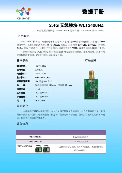
2.4G无线模块WLT2408NZ产品数据手册编号:DSWLT01003 更新日期:2012/04/26 版本:V1.03产品概述WLT2408NZ模块是广州晓网电子出品的WLT系列ZigBee数据传输模块,具备最大8dBm 输出功率,视距传输距离可达500米(@5dbi天线),工作频段2.380GHz~2.500Ghz,除标准ZigBee的16个通道外,还有9个扩展频段,可以有效避开WIFI、蓝牙等其他2.4G信号干扰。
广州晓网电子为WLT2408NZ用户提供mesh对等无线路由协议,无组网延时,采用时间空间权值均衡原则,路由时间短,通讯稳定可靠。
基本参数产品图片输出功率:供电电压:天线接口:数字接口:视距传输距离:功耗:休眠电流工作温度:存储温度:尺寸:-50~+8dBm1.9~3.3VSMA,U.FLUART,GPIO,AD500米@5dbi天线发送峰值电流46.3mA,接收时36.4mA <1uA-40℃至+85℃-40℃至+105℃16×23mm公司简介广州晓网电子科技有限公司是一家专门从事无线通讯方案设计、生产及服务的公司,公司拥有一流的设计团队,运用先进的工作方法,集合无线设计经验,公司拥有业界实用的各种模块,也为客户提供客制化服务。
订货信息WLT2408NZ-S SMA形式天线接头WLT2408NZ-U U.FL形式天线接头WLT2408NZ SDK 无线模块评估板套件,包含两个评估板,搭载的模块为WLT2408NZ-S。
数据手册版权声明本文档提供有关晓网电子产品的信息,并未授予任何知识产权的许可,并未以明示或暗示,或以禁止发言或其它方式授予任何知识产权许可,任何单位和个人未经版权所有者授权不得在任何形式的出版物中摘抄本手册内容。
产品命名规则图1-1 产品命名规则例如:WLT2408NZ-S表示晓网电子模块类的产品,频段为2.4GHz,理论输出功率为﹢8dBm(实际输出为﹢7.7dBm),超小封装,调制方式为ZigBee,外置SMA头的模块。
ZIGBEE模块分类选型指导模块分类标准很多,初学者往往无法下手,这里文档主要针对种类对文档进行区分,方便用户根据自己需要,选择不同类型的模块;¾应用要求:分开发系列和固化系列;ZIGBEE模块是带处理器内核的SOC器件,可以理解为(单片机+射频收发器);用户若自己开发模块内部程序,可选择开发系列;如选用已开发好特定功能的模块,可选择固化系列;¾天线引出类型:分PCB天线、IPEX天线、SMA天线;PCB为板载天线,其余为外置天线;¾是否带射频前端:带射频前端的模块,增大了发射功率,优化了接收灵敏度,传输距离更远些;¾模块封装:分直插(排针)和贴片(邮票孔)两种类型。
¾QAZ2000/QAZ2000X透传模块内置固件,用于将UART串口(TTL电平)转为ZIGBEE无线进行数据收发。
参数指标工作电压DC +3.3V(2.6V~3.6V)温度范围-40℃-- +85℃串口速率38400bps(默认),用户可通过串口指令修改为2400、4800、9600、19200、38400、57600、115200无线频率2405MHz(默认),用户可通过串口指令软件修改,2405MHz~2480MHz,步进5M,共16个信道无线协议Zigbee2007/PRO节点类型出厂默认为路由器,用户可任意配置为协调器或路由器传输距离空旷环境1600米(最大)发射电流135mA(最大)接收电流30mA(最大)平均电流45mA(典型)外形尺寸 26*36mm净 重 5.4g主控芯片CC2530F256接口方式UART(3.3V )串口发TX、串口收RX可直接驱动RS232转UART(3.3V)芯片可直接驱动USB转UART(3.3V)芯片可直接驱动RS485转UART(3.3V)芯片,内置RS485方向控制¾QAZV1/QAZV1X透传模块内置固件,用于将UART串口(TTL电平)转为ZIGBEE无线进行数据收发。
NZB1730系列模块规格书V1.00版权声明本手册版权归属上海纳普信息科技有限公司(简称“纳普科技”)所有,并保留一切权利。
非经纳普科技书面同意,任何单位及个人不得擅自摘录本手册部分或全部内容。
免责声明由于产品版本升级或其他原因,本手册内容会不定期更新。
除非另有约定,本手册仅作为使用指导,本手册所有陈述、信息和建议不构成任何明示或暗示的担保。
商标声明为上海纳普信息科技有限公司的商标。
本文提及其他所有商标和注册商标,归各自的所有人所有。
目录1产品概述 (4)1.1产品简介 (4)1.2产品外形 (4)1.3产品特性 (4)2产品功能说明 (5)2.1原理框图 (5)2.2 DEBUG接口说明 (6)2.3 UART接口说明 (6)2.4接口极限应用条件 (7)2.5接口推荐应用条件 (7)2.6电源特性 (7)2.7温度特性 (8)2.8天线特性 (8)2.8.1天线接口 (8)2.8.2陶瓷天线辐射特性 (9)3设计注意事项 (9)4结构与安装 (10)1产品概述1.1产品简介NZB1730模块是上海纳普信息科技推出的一款嵌入式ZigBee无线通信模块,集成了符合ZigBee Pro标准的射频收发器和应用软件。
1.2产品外形NZB1730 ZigBee模块外形规格,如表1-1所示。
表1-1 NZB1730 ZigBee模块外形规格外形规格参数尺寸(长×宽×高)15mm×26mm×0.8mmNZB1730 ZigBee模块正面图和背面图分别如图1-1和图1-2所示。
图1-1 NZB1730正面图图1-2 NZB1730背面图1.3产品特性NZB1730系列ZigBee模块产品特性参数,如表1-2所示。
表1-2 NZB1730 ZigBee模块产品特性参数产品特性参数工作频段2405~2480MHz最大发射功率4dBm最大室外无障碍通讯距离50m最大室外无障碍组网距离150 m接收灵敏度-97dBm工作温度-40℃~+ 125℃电源电压+2.0V~+3.6V(推荐值+3.3V)产品特性描述待机电流12mA(无睡眠)工作电流27mA(TX)25mA(RX)协议ZigBee HA/ ZigBee Light Link Zigbee2007 /Zigbee Pro2产品功能说明2.1原理框图由上图2-1所示,NZB1730模块电路主要由主控集成电路TI-CC2530F256和功率放大集成电路TI-CC2592R所组成,并含有贴片天线。
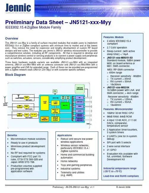
Preliminary Data Sheet – JN5121-xxx-MyyIEEE802.15.4/ZigBee Module FamilyPreliminary - JN-DS-JN5121-xxx-Myy v1.1 © Jennic 2006OverviewThe JN5121-xxx-Myy is a family of surface mounted modules that enable users to implement IEEE802.15.4 or ZigBee compliant systems with minimum time to market and at the lowest cost. They remove the need for expensive and lengthy development of custom RF board designs and test suites. The modules use Jennic’s JN5121 wireless microcontroller to provide a comprehensive solution, including all RF components. All that is required to develop and manufacture wireless control or sensing products is to connect a power supply and peripherals such as switches, actuators, sensors, considerably simplifying product development.Three basic hardware module variants are available: JN5121-xxx-M00 with an integrated antenna, JN5121-xxx-M01/M03 with an antenna connector and JN5121-xxx-M02/M04 with a power amplifier and LNA for extended range. Each of these can be provided pre-programmed with a ZigBee network stack (JN5121-Z01-Myy) or with customer-specific software.Block DiagramJennicii Preliminary - JN-DS-JN5121-xxx-Myy v1.1 © Jennic 2006Contents1. Introduction11.1.Variants12. Specifications 23. Product Development33.1. JN5121 Single Chip Wireless Microcontroller 34. Pin Configurations 44.1. Pin Assignment 5 4.2. Pin Descriptions 6 4.3. Power Supplies6 4.4.SPI Memory Connections6 5. Electrical Characteristics75.1. Maximum Ratings 7 5.2. Operating Conditions7 Appendix A Mechanical and Ordering Information 8 A.1 Outline Drawing8 A.2 Module PCB Footprint 11 A.3 Ordering Information 12 A.4 Accessories13 A.5 Tape and Reel Information:14 A.5.1 Tape Orientation and dimensions 14 A.5.2 Cover tape details 14 A.5.3 Leader and Trailer 15 A.5.4 Reel Dimensions: 15 A.6 Related Documents 16 A.7 Disclaimers 17 A.8 Version Control 17 A.9 Contact Details18Jennic Jennic© Jennic 2006 Preliminary - JN-DS-JN5121-xxx-Myy v1.1 11. IntroductionThe JN5121-xxx-Myy module family provides designers with a ready made component which allows IEEE802.15.4 [1]wireless applications, including ZigBee, to be quickly and easily included in product designs. The modules integrate all of the RF components, removing the need to perform expensive RF design and test. Products can be designed by simply connecting sensors and switches to the module IO pins. The modules use Jennic’s single chip IEEE802.15.4 Wireless Microcontroller, allowing designers to make use of the extensive chip development support material. Hence, this range of modules allows designers to bring wireless applications to market in the minimum time with significantly reduced development effort and cost.Three basic modules are available: JN5121-xxx-M00 (standard module with on board ceramic antenna), JN5121-xxx-M01 (standard module with SMA connector for use with external antennae) and JN5121-xxx-M02 (high RF power, improved sensitivity module for extended range applications). Each of these modules can be supplied with a range of protocol stacks, including a simple IEEE802.15.4 protocol for point to point and star applications and a ZigBee mesh networking stack. The variants available are described below.1.1. VariantsVariantDescriptionJN5121-000-M00 JN5121 Module (IEEE802.15.4 stack, ceramic antenna) JN5121-Z01-M00 JN5121 Module (ZigBee stack, ceramic antenna) JN5121-000-M01 JN5121 Module (IEEE802.15.4 stack, SMA connector) JN5121-Z01-M01 JN5121 Module (ZigBee stack, SMA connector)JN5121-000-M02 JN5121 Module (High Power (18.5dBm), IEEE802.15.4 stack, SMA connector) JN5121-Z01-M02 JN5121 Module (High Power (18.5dBm), ZigBee stack, SMA connector) JN5121-000-M03 JN5121 Module (IEEE802.15.4 stack, RP-SMA connector) JN5121-Z01-M03 JN5121 Module (ZigBee stack, RP-SMA connector)JN5121-000-M04 JN5121 Module (High Power (18.5dBm), IEEE802.15.4 stack, RP-SMA connector) JN5121-Z01-M04JN5121 Module (High Power (18.5dBm), ZigBee stack, RP-SMA connector)Jennic2 Preliminary - JN-DS-JN5121-xxx-Myy v1.1 © Jennic 20062. SpecificationsMost specification parameters for the modules are specified in JN-DS-JN5121 Datasheet for JN5121 single chip wireless microcontroller, [2]. Where there are differences, the parameters are defined here. VDD=3.0V @ +25ºCTyp. DC CharacteristicsNotesJN5121-xxx-M00/01/03 JN5121-xxx- M02/04 Deep sleep <11uA <11uASleep <14uA <14uA With active sleep timer Radio transmit 44mA 115mA CPU in doze, radio transmitting Radio receive49mA 60mA CPU in doze, radio receiving Centre frequency accuracy+/-25ppm+/-25ppmAdditional +/-15ppm allowance for temperature and agingTyp. RF CharacteristicsNotesReceive sensitivity -90dBm -93dBm Nominal for 1% PER, as per 802.15.4 section 6.5.3.3 Max. Transmit power 0dBm 16dBm Nominal Transmit power at 3.6V 18.5dBm With Vcc=3.6VMaximum input signal -10dBm-15dBm For 1% PER, measured as sensitivity RSSI range-95 to -10 dBm -115 to -20 dBmRF Port impedance - SMA connector 50 ohm 50 ohm 2.4 - 2.5GHz VSWR (max)2:12:12.4 - 2.5GHzPeripheralsNotesMaster SPI port with five select outputs 250kHz - 16MHz Slave SPI port 250kHz - 16MHz Two UARTs16550 compatible Two-wire serial I/F (compatible with SMbus & I 2C) Up to 400kHz Two programmable Timer/Counters with capture/compare facility, Tick timer 16MHz clock Two programmable Sleep Timers32kHz clock Twenty-one digital IO lines (multiplexed with UARTs, timers and SPI selects)Four-channel, 12-bit, Analogue-to-Digital converterUp to 100ks/s Two 11-bit Digital-to-Analogue converters Up to 100ks/sProgrammable analogue comparatorUltra low power mode for sleepInternal temperature sensor and battery monitorJennic Jennic© Jennic 2006 Preliminary - JN-DS-JN5121-xxx-Myy v1.1 33. Product DevelopmentJennic supplies all the development tools and networking stacks needed to enable end product development to occurquickly and efficiently. These are all freely available from Jennic’s support website: /support/ . A range of evaluation/developer kits is also available, allowing products to be quickly breadboarded. Efficient development of software applications is enabled by the provision of a complete, unlimited, software developer kit. Together with the available libraries for the IEEE802.15.4 MAC and the ZigBee network stack, this package provides everything required to develop application code and to trial it with hardware representative of the final module. The modules can be programmed by the user, for both development and production, using Jennic supplied software. They can also be supplied ready loaded with customer defined software if required. The JN-UG-3007 Flash Loader User Guide [5], describes how to put the module into programming mode, download software onto the module and to load individual MAC addresses. Access to the on-chip peripherals, MAC and ZigBee stack software is provided through specific APIs. These are described in the JN-RM-2001 Hardware Peripheral Library Reference Manual [3], JN-RM-2002 Stack Software Reference Manual [4] and JN-RM-2014 ZigBee Application Development API Reference Manual [6]. Additional information is available on the Jennic support website.3.1. JN5121 Single Chip Wireless MicrocontrollerThe JN5121-xxx-Myy series is constructed around the JN5121 single chip wireless microcontroller, which includes the radio system, a 32-bit RISC CPU, ROM and RAM memory and a range of analogue and digital peripherals. The chip is described fully in JN-DS-JN5121 Datasheet for JN5121 single chip wireless microcontroller [2].Jennic4 Preliminary - JN-DS-JN5121-xxx-Myy v1.1 © Jennic 2006ADC4DAC1DAC2COMP+COMP-SPICLK SPIMISO SPIMOSI SPISSZDIO0/SPISEL1DIO1/SPISEL2DIO2/SPISEL3SPISSM SPISWP DIO3/SPISEL4D I O 4/C T S 0D I O 5/R T S 0D I O 6/T X D 0D I O 7/R X D 0D I O 8/T I M 0G T D I O 9/T I M 0_C A PD I O 10/T I M 0_O U T D I O 11/T I M 1G TV D D G N D V S S AADC3ADC2ADC1NC NCDIO20/RXD1DIO19/TXD1DIO18/RTS1DIO17/CTS1DIO16DIO15/SIF_D RESETNDIO14/SIF_CLK DIO13/TIM1_OUT DIO12/TIM1_CAPFigure 1: Pin Configuration (top view)Note that the same basic pin configuration applies for all module designs. However, DIO3/SPISEL4 and DIO2/SPISEL3 are not available with high power modules.Jennic Jennic© Jennic 2006 Preliminary - JN-DS-JN5121-xxx-Myy v1.1 54.1. Pin AssignmentModulePin SignalFunctionAlternative Function1 ADC4 Analogue to Digital input2 DAC1 Digital to Analogue output3 DAC2 Digital to Analogue output4 COMP+5 COMP- Comparator inputs6 SPICLK SPI master clock out/slave clock in7 SPIMISO SPI Master In/Slave Out8 SPIMOSI SPI Master Out/Slave In9 SPISSZ SPI select from module - SS0 (output)10 SPISEL1 SPI Slave Select1 (output) General Purpose Digital I/O DIO0 11 SPISEL2 SPI Slave Select2 (output) General Purpose Digital I/O DIO1 12 SPISEL3* SPI Slave Select3 (output) General Purpose Digital I/O DIO2 * 13 SPISSM SPI select to FLASH (input)14 SPISWP FLASH write protect (input) 15 SPISEL4* (not on Hi SPI Slave Select4 (output) General Purpose Digital I/O DIO3* 16 CTS0 UART0 Clear To Send (input) General Purpose Digital I/O DIO4 17 RTS0 UART0 Request To Send (output) General Purpose Digital I/O DIO5 18 TXD0 UART0 Transmit Data (output) General Purpose Digital I/O DIO6 19 RXD0 UART0 Receive Data (input) General Purpose Digital I/O DIO7 20 TIM0GT Timer0 clock/gate (input) General Purpose Digital I/O DIO8 21 TIM0_CAP Timer0 capture (input) General Purpose Digital I/O DIO9 22 TIM0_OUT Timer0 PWM (output) General Purpose Digital I/O DIO10 23 TIM1GT Timer1 clock/gate (input) General Purpose Digital I/O DIO11 24 VDD 3V power 25 GND Digital ground 26 VSSA Analogue ground 27 TIM1_CAP Timer1 capture (input) General Purpose Digital I/O DIO12 28 TIM1_OUT Timer1 PWM (output) General Purpose Digital I/O DIO13 29 RESETN Active low reset30SIF_CLKSerial Interface clock / Intelligent peripheral clockGeneral Purpose Digital I/O DIO14Jennic6 Preliminary - JN-DS-JN5121-xxx-Myy v1.1 © Jennic 2006ModulePin SignalFunctionAlternative Function31 SIF_D Serial Interface data / Intelligent peripheral data outGeneral Purpose Digital I/O DIO15 32 DIO 16 Intelligent peripheral device select General Purpose Digital I/O 33 CTS1 UART1 Clear To Send (input) General Purpose Digital I/O DIO17 34 RTS1 UART1 Request To Send (output) General Purpose Digital I/O DIO18 35 TXD1 UART1 Transmit Data (output) General Purpose Digital I/O DIO19 36 RXD1 UART1 Receive Data (input) General Purpose Digital I/O DIO2037 NC 38 NC Connect to ground39 ADC1 Analogue to Digital input 40 ADC2 Analogue to Digital input 41ADC3Analogue to Digital input *: These two pins are not connected for High power modules4.2. Pin DescriptionsAll pins behave as described in the JN5121 datasheet [2], with the exception of the following:4.3. Power SuppliesA single power supply pin, VDD is provided. Separate analogue (VSSA) and digital (GND) grounds are provided. These should be connected together at the module pins.4.4. SPI Memory ConnectionsSPISWP is a write protect pin for the serial flash memory. This should be held low to inhibit writes to the flash device. SPISSZ is connected to SPI Slave Select 0 on the JN5121. SPISSM is connected to the Slave Select pin on the memory.This configuration allows the flash memory device to be programmed using an external programmer if required. The JN5121 should be held in reset by taking RESETN low. The memory can then be programmed over the UART by using the programming mode described in JN-UG-3007 Flash Loader User Guide [5]. Alternatively, the memory can be programmed by connecting a SPI programmer to SPISSM, SPICLK, and SPIMISO and directly loading the code into the memory.For normal operation of the module, SPISSZ should be connected to SPISSM.Jennic Jennic© Jennic 2006 Preliminary - JN-DS-JN5121-xxx-Myy v1.1 75. Electrical CharacteristicsIn most cases, the Electrical Characteristics are the same for both module and chip. They are described in detail inthe chip datasheet. Where there are differences, they are detailed below.5.1. Maximum RatingsExceeding these conditions will result in damage to the device.ParameterMin Max Device supply voltage VDD1, VDD2 -0.3V3.6VVoltage on analogue pins ADC1-4, DAC1-2, COMP2M, COMP2P-0.3V VDD + 0.3VVoltage on 5V tolerant digital pins SPICLK,SPIMOSI, SPIMISO, SPISEL0, GPIO0-GPIO20, RESETN-0.3VVDD + 2V or 5.5V, whichever is the lesserStorage temperature-40ºC 150ºC Solder reflow temperature (According to IPC/JEDEC J-STD-020C)260 °CThis device is sensitive to ESD and should only be handled using ESD precautions.5.2. Operating ConditionsSupplyMin Max VDD2.7V3.6V Ambient temperature range-20ºC70ºCJennic8 Preliminary - JN-DS-JN5121-xxx-Myy v1.1 © Jennic 2006Appendix A Mechanical and Ordering InformationA.1 Outline Drawingmm2.54mmmm1.27mmThickness: 3mmJN5121-xxx-M00 Outline Drawing2.79 mm 2.54 mm2.54 mm 1.27 mmThickness: 3mm over can, 10.6mm at SMA connectorJN5121-xxx-M01/M03 Outline Drawingmm 1.27 mmmmThickness: 3mm, 10.6mm at SMA connectorJN5121-xxx-M02/M04 Outline DrawingA.2 Module PCB FootprintAll Pads are 0.9mm square on 1.27mm pitch1.27mmNote: All modules have the same footprint.A.3 Ordering InformationPart Numbering:Software Variant000 IEEE802.15.4 Stack Z01 ZigBee StackShippingR Box (10 modules per pack) T Tape Mounted 500pcs (00 module only) V Tape Mounted 200pcs (01,02,03,04 modulesonly)Temp Range / Device Status D -20°C to +70°C, QualifiedModule Type 00 Standard Power, Ceramic antenna 01 Standard Power, SMA connector 02 High Power, SMA connector 03 Standard Power, RP-SMA connector 04 High power, RP-SMA connectorA.4 AccessoriesProduct DescriptionNoteJNAC001 JN5 serial level converter dongleConnects module UART port to PC serial port to allow code development and debugThe JNAC001 RS-232 level converter is used to translate the +/- 7V RS-232 levels to CMOS compatible logic levels.The CMOS levels are made available through a short flying lead with a 6-way IDC socket. This can be connected to the relevant module UART0 pins. The RS-232 Interface is available on a standard nine-way ‘D’ connector.J1C T R R TD SFigure 5-1: JNAC001 RS-232 Converter Connection26View looking at cableconnectorFigure 5-2: RS-232 ConnectorA.5 Tape and Reel Information:A.5.1 Tape Orientation and dimensionsModule type: A B W F E P0 P1 P2 T Cover Tapewidth (W) JN5121-xxx-M00 18.4 30.4 44 20.2 1.75 4.0 2.0 24.0 3.2 37.5JN5121-xxx-M01/3 18.4 30.4 56 20.2 1.75 4.0 2.0 24.0 11.4 49.5JN5121-xxx-M02/4 18.4 40.5 56 20.2 1.75 4.0 2.0 24.0 11.4 49.5 Tolerance ±0.1 ±0.1 ±0.3 ±0.1 +0.1 ±0.1 ±0.1 ±0.1 ±0.1A.5.2 Cover tape detailsThickness (T) 0.061mmSurface resistivity (component side) 104 to 107 Ohms/sqSurface resistivity (component side) Non-conductiveBacking type: PolyesterAdhesive type: PSASealing: Room ambientA.5.3 Leader and TrailerA.5.4 Reel Dimensions:Module type: A B C N W (min)JN5121-xxx-M00 330 ±1.0 2.2±0.5 13 ±0.2 100 +0.1 44.5 ±0.3JN5121-xxx-330 ±1.0 2.2±0.5 13 ±0.2 100 +0.1 56.5 ±0.3 M01/02/03/04A.6 Related Documents[1] IEEE Std 802.15.4-2003 IEEE Standard for Information Technology – Part 15.4 Wireless Medium Access Control(MAC) and Physical Layer (PHY) Specifications for Low-Rate Wireless Personal Area Networks (LR-WPANs)[2] JN-DS-JN5121 Datasheet for JN5121 single chip wireless microcontroller[3] JN-RM-2001 Hardware Peripheral Library Reference Manual[4] JN-RM-2002 Stack Software Reference Manual[5] JN-UG-3007 Flash Loader User Guide[6] JN-RM-2014 ZigBee Application Development API Reference ManualRoHS ComplianceJN5121-xxx-Myy devices meet the requirements of Directive 2002/95/EC of the European Parliament and of the Council on the Restriction of Hazardous Substance (RoHS).Status InformationThe status of this Data Sheet is Preliminary.Jennic products progress according to the following format:AdvanceThe Data Sheet shows the specification of a product in planning or in development.The functionality and electrical performance specifications are target values and may be used as a guide to the final specification.Jennic reserves the right to make changes to the product specification at anytime without notice.PreliminaryThe Data Sheet shows the specification of a product that is in production, but is not yet fully qualified.The functionality of the product is final. The electrical performance specifications are target values and may used as a guide to the final specification. Modules are identified with an R suffix, for example JN5121-Z01-M00R.Jennic reserves the right to make changes to the product specification at anytime without notice.ProductionThis is the final Data Sheet for the product.All functional and electrical performance specifications, including minimum and maximum values are final.This Data Sheet supersedes all previous document versions.Jennic reserves the right to make changes to the product specification at anytime to improve its performance.A.7 DisclaimersThe contents of this document are subject to change without notice. Jennic reserves the right to make changes, without notice, in the products, including circuits and/or software, described or contained herein in order to improve design and/or performance. Information contained in this document regarding device applications and the like is intended through suggestion only and may be superseded by updates. It is your responsibility to ensure that your application meets with your specifications.Jennic assumes no responsibility or liability for the use of any of these products, conveys no license or title under any patent, copyright, or mask work right to these products, and makes no representations or warranties that these products are free from patent, copyright, or mask work infringement, unless otherwise specified.Jennic products are not intended for use in life support systems, appliances or systems where malfunction of these products can reasonably be expected to result in personal injury, death or severe property or environmental damage. Jennic customers using or selling these products for use in such applications do so at their own risk and agree to fully indemnify Jennic for any damages resulting from such use.All trademarks are the property of their respective owners.A.8 Version ControlVersion Notes0.9 1st Issue of Preliminary Datasheet1.0 Update performance parameters & Ordering / Tape & Reel informationA.9 Contact Details Corporate HeadquartersJennic Ltd, Furnival StreetSheffield S1 4QT, UKTel: +44 (0)114 281 2655Fax: +44 (0) 114 281 2951***************Jennic Ltd JapanOsakaya building 4F1-11-8 Higashigotanda Shinagawa-ku Tokyo 141-0022, JapanTel: +81 3 5449 7501Fax: +81 3 5449 0741**************.comJennic Ltd Taiwan19F-1, 182, Sec.2 Tun Hwa S. Road. Taipei 106, TaiwanTel: +886 2 2735 7357Fax: +886 2 2739 5687**************.comJennic America Inc - East Coast Office 1322 Scott Street, Suite 203Point Loma, CA 92106, USATel: +619 223 2215Fax: +619 223 2081**************.comJennic America Inc - West Coast Office 1060 First Avenue, Suite 400King of Prussia, PA 19406, USATel: +1 484 868 0222Fax: +1 484 971 5015**************.com。
广州致远电子有限公司AW516x串口转ZigBee 无线模块修订历史目录1. 产品简介 (3)1.1产品简介 (3)1.2产品命名规则 (3)1.3产品选型 (4)2. 尺寸图 (5)3. 接口 (6)3.1引脚排列 (6)3.2引脚说明 (6)4. FastZigBee组网协议 (8)4.1FastZigBee协议特点 (8)4.2节点类型说明 (9)4.3软件基本配置参数 (10)5. 驱动安装指南 (12)5.1CP210x驱动程序下载 (12)5.2CP210x驱动程序安装 (12)6. 快速使用指南 (16)7. 命令配置 (19)7.1临时参数配置协议与命令 (19)7.2永久参数配置协议与命令 (21)免责声明 (36)1. 产品简介1.1 产品简介AW516x是广州致远电子基于NXP JN516X无线微控制器开发的一系列低功耗、高性价比的ZigBee模块,并提供一个完整的基于IEEE802.15.4标准ISM频段的应用集成方案。
产品经过系列权威射频仪器的检验和认证,并结合多年的市场经验和该行业用户的实际需求,将无线产品极复杂的通讯协议集成到内置的MCU中,支持串口透明传输模式,并集成快捷易用的自组网功能,提供多路用户可配置的AD、IO、PWM接口,化繁为简,大幅简化无线产品复杂的开发过程,使您的产品以更低的成本快速投入市场,由于超小的体积和超低功耗设计,在各种智能设备中得到广泛应用。
图1.1 AW516x系列ZigBee无线模块实物图1.2 产品命名规则AW516x系列模块的命名规则,如图1.2所示。
本系列所有模块出厂默认参数均遵循产品命名规则,在购买产品前请务必确认产品型号是否与需求一致。
图1.2 产品命名规则表1.1 AW516x系列模块产品型号一览表注②:模块视距通信距离(外接天线版):P0≈150m,P1≈300m,P2≈2km;注③:板载天线模块一般需嵌入到用户产品当中,通信距离请根据实际应用实测。
ZT-2055ZigBee Wireless Module with 8-ch Digital Input and 8-ch Digital Output ModuleQuick Start GuideProduct Website:https:///zt_2055.htmlIntroductionThe ZT-2055 offers 8 isolated channels for digital input and 8 isolated channels for digital output. Either sink-type or source-type digital input can be selected via wire connections. All digital input channels are also able to be used as 16-bit counters. The ZT-2055 supports source-type output with short circuit protection. There are options for configuring power-on and safe digital output values. The ZT-2055 has 16 LED indicators to display the channel status, and has 4 kV ESD protection and 2500 VDC intra-module isolation. Users can easily configure the module address, protocol, checksum, ZB-PID and ZB-channel settings using a combination of rotary and DIP switches.The shipping package contains the following items:ZT‐2055 DIO Device ANT‐124‐05 Quick Start2 Preparing the Device1. Refer the chapter 3. to configure the DIP switch of ZT-2055 I/O device.2. Install the ZT Configuration Utility to configure the ZT-2055 coordinator. CD:\Napdos \ZigBee \ZT_Series \Utility /pub/cd/usbcd/napdos/zigbee/zt_series/utility3. Power Supply: +10 ~ +30 V DC3.1Introduction to the Configuration ParametersA.“Pan ID” parameter is the group identity for a ZigBee network, and must the samefor all devices in the same ZigBee network.“Address/Node ID” parameter is the individed identity of a specific the ZigBeemodule, and must be unique for each device connected the same ZigBee network.B.“RF Channel” parameter indicates the radio frequency channel, and must be set to thesame value as other modules on the same ZigBee network.Channel0x000x01……0x0FFrequency(MHz)24052410 (2480)※RF channels 0x04, 0x09, 0x0E or 0x0F are recommended because they do not overlap with the Wi-Fi frequencies based.802.11b/g802.11b/gChannel 1Channel 62400 000102030405060708090A0B0C0D0E0F 2485MHz MHz802.11b/g Channel (North America)802.15.4 ChannelC. Protocol/Application Mode:When implementing custom programs based on different protocols, the following application modes are recommended in order to ensurecommunicatibleUser Program Protocol DCONModbus RTUModbus TCP ZT-2055 I/O ZT-2550ZT-2570 DCON Transparent TransparentModbus RTUTransparent TransparentModbus Gateway Modbus Gateway Modbus RTU------Modbus Gateway4 Rotation Switch and DIP SwitchThe configuration of ZT-2055 series can be adjusted by using the external rotary switch and the DIP switches. The ZT-2055 device should only be rebooted once the configuration is complete.DIP Switch to the ZT‐2042/ZT‐2043/ZT‐2055/ZT‐2055Protocol Pan ID123456789101112 Address LSB Address MSBChecksum RF Channel Reserved (Node ID)(Node ID)DIP Switch to the ZT‐2055/ZT‐2060Pan IDProtocolAddress LSB Address MSBChecksum RF Channel (Node ID)(Node ID)ZT-2055 - 8-channel DI DAQ module - QuickStart (Dec/2019)ICP DAS USA, Inc. | | 1-310-517-9888 | 24309 Narbonne Ave. Suite 200. Lomita, CA 90717※Once the address of hardware switch is set to 0x00, it mens the address is using software configurations. Refer the more detailed information at Sec. 6.6 of user manual.DIP SwitchNumber Item Status Explain1Address MSB OFF Valid Address (Node ID) from 0x00 to 0x0F ON Valid Address (Node ID) from 0x10 to 0x1F2Protocol OFF DCON ProtocolON Modbus RTUProtocol3Checksum OFF Disabled ON Enabled4ZigBee Pan ID OFF Pan ID = 0x0000 ON Pan ID = 0x00015OFF------ON0x086OFF------ZigBee ON0x04 RF Channel7OFF------ON0x028OFF------ON0x01ZT-2055 - 8-channel DI DAQ module - QuickStart (Dec/2019)ICP DAS USA, Inc. | | 1-310-517-9888 | 24309 Narbonne Ave. Suite 200. Lomita, CA 90717As the ZigBee network is controlled by the ZigBee coordinator, the ZT-2550/ZT-2570 (ZigBee coordinator) must be configured first. Please refert to documents shown below for full details of how to configure these devices.Once configuration of the ZigBee coordinator has been completed. Set the ”Pan ID” and the “RF Channel” values for the ZT-2000 I/O device to the same values as the network, and then reboot the device. The module will automatically start to function on the ZigBee network using the default protocol.※Configuration Utility (Used to configure ZT-2000 I/O device Coordinator)/pub/cd/usbcd/napdos/zigbee/zt_series/utility/ZT-2055 - 8-channel DI DAQ module - QuickStart (Dec/2019)ICP DAS USA, Inc. | | 1-310-517-9888 | 24309 Narbonne Ave. Suite 200. Lomita, CA 90717ZT-2055 - 8-channel DI DAQ module - QuickStart (Dec/2019) ICP DAS USA, Inc. | | 1-310-517-9888 | 24309 Narbonne Ave. Suite 200. Lomita, CA 90717Configurations of ZT‐2550/ZT‐2570Configurations of ZT-2000 I/O DeviceNumber ItemStatus Explain1 Address MSB OFF Address/Node ID is 01(Rotation Switch=1)2 Protocol ON Use Modbus RTU Protocol3 Checksum OFF Disabled4 ZigBee Pan ID OFF Pan ID=0x0000 5ON 0x08 6 ZigBeeON0x04ZigBee RF Channel = 0x0E 7RF ChannelON0x02 8OFF------Once the ZT-2000 I/O device has joined the ZigBee network, the signal quality can be comfirmed by monitoring the status of the ZigBee Net LED indicators. If the LED indicator shows a steady light, communication with the ZT-2000 I/O device has been successfully established for data acquisition and control.ICP DAS also provides the “DCON Utility”, which can be used to simulate DCON/Modbus communication. This software can also be used to verify the device settings and ZigBee I/O functions.※The DCON Utility can be dowmload from:/pub/cd/8000cd/napdos/driver/dcon_utility/Simulate I/O channel operating via using DCON Utilityunch DCON Utility and select the correct COM Port settings to connect theZigBee Coordinator (ZT-2550/ZT-2570).2.Clicking “Search” button will start searching which ZT-2000 I/O device is in thesame ZigBee network.3.If there is any ZT-2000 I/O devices displayed, double clicking the “modulename” will start the I/O channels operated platform.ZT-2055 - 8-channel DI DAQ module - QuickStart (Dec/2019)ICP DAS USA, Inc. | | 1-310-517-9888 | 24309 Narbonne Ave. Suite 200. Lomita, CA 90717ZT-2055 - 8-channel DI DAQ module - QuickStart (Dec/2019)ICP DAS USA, Inc. | | 1-310-517-9888 | 24309 Narbonne Ave. Suite 200. Lomita, CA 907178 Troubleshooting(1)Technical Support.If you have any difficulties using your ZT-2000 series I/O device, please send adescription of the problem to ******************Include the following items in your email:● A description or diagram of the current DIP switch positions.● A copy of the configuration file for the ZT-2000 coordinator. This file can beobtained using the procedure outlined below and should be attached to your email.a.Set the DIP switch of the ZT-255x device to the [ZBSET] position then reboot thedevice. Launch the ZT Configuration Utility and select [Save Log] icon to save the configuration of the ZT-255x as a file.b.After clicking the [Save Log] icon, enter the “File Name” and the “File Path” inthe Windows “Save” dialog box. Once the configuration has been successfullysaved, the following message will be displayed.c.(2)LED Indicator Status:LED Indicator Status IntroductionZigBee Router (Slave)Steady Lit The Signal is StrongBlinking (500 ms)The Signal is AvailableBlinking (1s)The Signal is WeakBlinking (2s)The Signal is Unstable or There is no AvailableThe status of module boardSteady Lit The Power is ON and the Module Initialization is CorrectZigBee PWR Blinking (200ms)Module Initialization Failure(Red LED)Watchdog is Enabled and the status of the I/O channel Blinking (1s)has been changed to the Safe Value. Reset the modulevia the power switch or configuration commands.Steady Unlit The Power is OFFThe status of DI/DO channelsZigBee DI/DO Steady Lit The DI/DO channel is EnabledSteady Unlit The DI/DO channel is Disabled。
ZigBee模块产品数据手册广州星博信息技术有限公司Guangzhou Great Symbol Information Technology Co.,Ltd一、概述ZigBeee模块分为基本型和增强,增强型/基本型模块开放了许多外设端口,两个模块的引脚完全兼容,可以通过SDK对模块进行配置后,使用其相应的外设端口,实现数据的采集、外部设备的控制等,其上面有一个天线接口,用于外接天线。
增强型模块和基本型模块开放的外设端口有:基本型模组(1)1个串行通信接口(UART)(2)4个模拟量输入通道(ADC)(3)14个含复用的通用数字输入输出口(GPIO),不复用ADC/UART时最大为8个(复用:不使用UART/ADC功能时,所有IO可配置成GPIO)●增强型模组(1)42个含复用的通用数字输入输出口(GPIO),不复用ADC /DAC/ UART/ SPI/I2C/ CAN功能引脚时最大为9个(2)3个串行外设接口(SPI),其中1个复用ADC(3)2个内部集成总线接口(I2C),其中1个复用UART(4)1个工业现场总线接口(CAN)(5)4个串行通信接口(UART),其中1个复用I2C(6)12个模拟量输入通道(ADC),其中2个复用DAC,3个复用SPI(7)2个模拟量输出通道(DAC)(8)8个16位同步定时器二、产品特性●基本型模组◆尺寸:PCB贴片封装38.6*23.2*3mm◆重量:约3g◆电源:2V-3.6V 典型值:3.3V◆模块总功耗:A无线模块不工作时平均功耗12-13.5mWB无线模块工作时平均功耗97-121mWC无线模块工作时峰值功耗105-138mW◆天线功率:4dBm◆接收灵敏度:-97dBm◆电流:工作电流小于45mA ,待机电流小于1mA◆工作频率: 2.4G ISM频段◆环境温度:-20~75℃◆无线传输距离:200-250m(外接5dB鞭状天线),300-400m(外接9dB鞭状天线) 注:无线传输的距离测试时环境为:内部增益设定为4dB,空旷的环境下测出的直线距离,中间没有障碍物。
Core2530/XCore2530User Manual1.Introduction (2)2.Zigbee network experiment (4)2.1.Roles in Zigbee network (4)2.2.Bootloader (4)2.3.Firmware downloading (10)working communicaiton (12)3.Working with PC (15)3.1.Introduction (15)3.2.AT commands (15)Appendix (21)11.Core2530/XCore2530 is a Zigbee module developed by Waveshare, which adopts the CC2530 IC of TI as its main control chip. Comparing with Core2530, XCore2530 has a longer transmission distance by enhancing the power amplification function.This module can be used in two primary purposes:●For application (Users only need to concentrate themselves on application development,since this module works as a underlying hardware in this case):The firmware provided with the module should be applied. Under this condition, themodule would serve as a Zigbee wireless serial port. With the simple operations of themodule, as easy as that of the serial port, you do not need to know much about thecomplex Zigbee protocol.●For development (Users should perform a secondary development to the module forimplementing the underlying application):You need to write the Zigbee communication protocol code by yourself. In this case, youshould use the downloader, such as CC Debugger, and learn the Zigbee protocol.Features:●Simple operations, as easy as that of the serial port;●Self-networking (At least a coordinator and a router needed);●Severe as a router in factory default setting (modifiable to a coordinator by downloadingcorresponding coordinator firmware);●Support program download by serial port (the downloader is not required normally, sincethe firmware supports serial Bootloader);●Support parameter configuration by PC software;●RFX2401 power amplifier (XCore2530 only).2Core2530 XCore253032.Zigbee network needs minimum a coordinator and a router. Since the Core2530/XCore2530 module has a built-in Bootloader in default setting, you can download the firmware to the module directly via the serial port.Notes: In the Zigbee network experiment, you may need to apply two pieces of Core2530/XCore2530 modules, and two pieces of ZB502/ZB600 baseboards.2.1.ROLES IN ZIGBEE NETWORK1.Coordinator●Select a communication channel and a PAN ID to build a network;●Allow other routers and end devices to join this network;●Route the data in the network;●Must be kept power supplying, and must not enter the SLEEP mode;●Preserve data for the end devices entered SLEEP mode till them wake up and retrieve thedata.2.Router●Must join a Zigbee network before performing data transmission;●Allow other routers and end devices to join the network, after it joined one;●Route the data in the network upon joining the network;●Must be kept power supplying, and must not enter the SLEEP mode;●Preserve data for the end devices entered the SLEEP mode till them wake up and retrievethe data.3.End Device●Must join a Zigbee network before performing data transmission;●Not allow other devices to join the network;●Transmit and receive data thought parent node, unable to route the data in the network;●Support battery power supply and SLEEP mode.2.2.BOOTLOADER1.IntroductionThe built-in Bootloader enable users to download the program to the module directly via a serial port without using the CC Debugger. However, the CC Debugger is required in the course of programming4the Bootloader into the module. For more detailed information, please refer to the Section How to program Bootloader.There are two different Bootloaders available for this module: bootloader.hex and bootloader_wait.hex.For easier understanding, we call the module with the bootloader.hex as module A, and the module with the bootloader_wait.hex as module B in this document.The module A will execute the valid program immediately, if any, in the Flash memory, after powered up. Otherwise, its LED1 will keep blinking indicating that there is no program in the Flash memory and you can download a new one via the serial port in this case.For module B, its LED1 and LED2 will blink alternately, if there is any valid program stored in the Flash memory, after powered up. Now, if you press the button KEY2, the module B will execute the program immediately; and if you press the button KEY1, the module B will enter the Bootloader mode under which you can download a new program to the module B. In case of no key-press action within 40 seconds after powered up, the module B will execute the program in the Flash memory automatically. When there is no valid program in the Flash memory, its LED1 will keep blinking, and you can download a new one via the serial port in this case.The module A with bootloader.hex is suitable for independent application, since it can run the program directly without any external key-press trigger. However, the module B with the bootloader_wait.hex should work with the baseboard ZB502/ZB600 for relative experiments and studies. By default, the bootloader_wait.hex is programmed to the module. debugger driver installation●Unzip the package CC-Debugger_Drivers.7zto the installation directory;●Double click the software Setup_SmartRF_Drivers-1.2.0.exe for installation;●5●●When finished, connect the CC Debugger to your PC, and open the option Device Managerin Windows. You may find the option CC Debugger if its driver is installed successfully.63.How to program Bootloader●Install the module to the baseboard, and connect the baseboard and the CC Debugger toyour PC with the USB cables;●Power up the baseboard, and press the RESET key on the CC Debugger. Ifthecommunication is built up successfully, the indicator on the CC Debugger will light up and turn to green, indicating that it is ready to download new programs;●Open the SmartRF Studio7the software interface to open another window.7Select the option Program CCxxxx Soc or MSP430 in the pulled-down menu What do you want to program?, and choose the image file you want to program within the Flash imagebox. Here, it isbootloader_wait.hex. And then,click the to start programming.89When finished, there will be a message “Erase, program and verify OK” appears on thebottom of the window, and the LED1 of the baseboard will keep blinking indicating that program downloading is successful.102.3. FIRMWARE DOWNLOADINGIn this section, we will illustrate how to build a Zigbee network by applying two groups of Core2530 + ZB600, one works as a coordinator and the other one works as a router. For easier understanding, we call the coordinator as Group A and the router as Group B.●Connect the Group A and the Group B to your PC with the USB cables, respectively. And get their corresponding serial port numbers after powered up. ● If the firmware has been installed to the Group A or/and the Group B, the LED1 and theLED2 on the Core2530 module(s) will blink alternately after resetting. Pressing the buttonfirmware in the Core2530 module(s), the LED1 will keep blinking after powered up, whichmeans the Core2530 module(s) has entered the Bootloader mode directly and there is no● Start the software SBDemo.exe for firmware downloading.11● Enter the corresponding serial port of the Group A in theCOM Port box, and click theCoordinator.bin in the Image Filebox. Then, click the●For the Group B, select the firmware file Router.bin . The file download method is the same as that of the Group A. ● Start two serial debug assistants, and enter the serial port number of the Group A to one ofthe assistants and the port number of the Group B to the other one. Then, set the Baud rate: 38400, Data bit: 8 and Stop bit: 1;● Reset the Group A, you can see the LED1 and the LED2 on its Core2530 module blinkalternately. Pressing the middle button of the joystick, you will see the message “Device starting ok ” displayed in the window and the LED3 lights up, if the network is built up successfully.● Reset the Group B, you can see the LED1 and the LED2 on its Core2530 module blinkalternately. Pressing the middle button of the joystick, you will see the message ““Device starting ok ” displayed in the window and the LED3 lights up, if the Group B, severing as a router, has joined the network successfully. Now, the Zigbee network is running.(Ifnoexternal antenna is applied to the Group B, it is recommended to place the antenna interface of the Group B close to the antenna interface of the Group A, in order to ensure the wireless network signal is strong enough.)Notes:ZB502.2. The power amplifier (PA) of Xcore2530 has occupied the Pins P1_1 and P1_4. Hence, theLED2 will not blinking after the Xcore2530 module reset, and the LED3 will keep OFF even if the network is built up successfully.WORKING COMMUNICAITONThe operations presented below can be done directly by UART serial communication.Broadcast communication modeDescription: Under this mode, a device can broadcast messages to all the other devices in the Zigbee network.Format: Data to be sentPoint to Point communicationDescription: It is the communication between any two nodes in the same network.12Format: P2P Target address Data to be sentPoint to Multipoint communicationDescription: A node sends data to the specified nodes in the same network.Format: O2M Quantity of target address Target address 1 Target address 2 … Data to be sent13143.3.1.INTRODUCTIONZBSCOMM is the PC software for Core2530/XCore2530 developed by Waveshare. With ZBSCOMM, you can easily configure the module settings and read the current configurations of the module via your PC. Of course, you can control the module by AT command as well, if you do not want to use the PC for configuration.3.2.AT COMMANDSTable 1: Restart the module15Table 2: Restore the factory settingsTable 3: Serial port information configuration16Table 4: Channel settingTable 5: Set the PAN ID17Table 6: Read all the configuration informationTable 7: Read the serial configuration informationTable 8: Read the current communication channel information18Table 9: Read the current PAN ID of the moduleTable 10: Read the short address of the deviceTable 11: Read the short address of the parent node19Table 12: Read the IEEE address of the deviceTable 13: Read the IEEE address of the parent node2021 1. ZB502ZB502 is a baseboard matching to the module Core2530/XCore2530. It contains an on-board battery socket which makes it possible to support different ways of power supply, an on-board CP2102 for customer debugging and program updating, and several LEDs and press-keys for basic operations. ZB502 leads out all its IOs, so users can easily make expansions on it.For more information about ZB502 baseboard, please refer to the links listed below:Chinese datasheet: /shop/ZB502.htmEnglish datasheet: /zb502.htm2.ZB600ZB600 is a baseboard matching to the module Core2530/XCore2530. It contains an on-board battery socket which makes it possible to support different ways of power supply, an on-board CP2102 for customer debugging and program updating, and several LEDs and press-keys for basic operations. ZB600 leads out all its IOs, so users can easily make expansions on it.Comparing with ZB502, ZB600 has some improvements: adding an AD conversion interface, a sensor interface, a LCD interface and a joystick.For more information about ZB600 baseboard, please refer to the links listed below:Chinese datasheet: /shop/ZB600.htmEnglish datasheet: /zb600.htm DebuggerThis product is an enhanced emulator/downloader designed by Waveshare. It is fully compatible with TI CC Debugger, and can provide an excellent hardware protection and human-friendly operation experience for users.CC Debugger can work with the TI SmartRF Flash Programmer for program downloading, and the TI SmartRF Studio for testing and debugging CCxxxx series devices. It can also cooperate with the IAR Embedded Workbench for 8051 to build up the development environment and implement seamless connection.22For more information about the CC Debugger, please refer to the links listed below:Chinese datasheet: /shop/CC-Debugger.htmEnglish datasheet: /cc-debugger.htm23。
©2023Guangzhou ZHIYUAN Electronics Co.,Ltd.ZM32-U 系列ZigBee 模块数据手册ZigBee 模块DS01010101 1.2Date:2023/5/30——————————————概述ZM32-U 系列ZigBee 模块是广州致远电子股份有限公司基于Silicon Labs 公司EFR32系列无线SoC 开发的低功耗、高可靠性的ZigBee 模块,它提供一个完整的基于IEEE802.15.4标准ISM (2.4~2.5GHz )频段的应用集成方案。
支持ZLGMesh 协议,可快速应用于工业控制、工业数据采集、农业控制、矿区人员定位、智能家居、智能遥控器等场合。
ZM32-U 系列ZigBee 模块,将完整的射频收发电路集成在一个模块上,将无线通讯产品复杂的通讯协议内嵌在内置的SoC 中,化繁为简,大幅简化开发过程,使得用户产品更快的投入市场,增加用户产品的竞争力,更好的把握住先机。
————————————产品应用◆ 工业控制◆ 工业数据采集◆ 农业控制◆ 矿区人员定位◆ 智能家居◆ 智能遥控器—————————————订购信息注:见选型表——————————产品特性◆频率范围:2400~2483.5MHz ◆工作电压:1.71~3.8V ◆接收电流:9.4mA ◆休眠电流:5.0uA ◆发射电流:185mA ◆发射功率:+20dBm ◆接收灵敏度:-103dBm ◆传输速率:250kbps◆IPEX 接口、邮票孔焊盘接口◆ 3.3V 接口电平◆采用UART 通信接口◆支持休眠及唤醒◆温度范围:-40~+85℃修订历史目录1.产品简介 (1)1.1概述 (1)1.2产品命名规则 (1)1.3产品选型 (2)2.外观尺寸 (3)3.引脚定义 (4)4.电气参数 (7)4.1工作条件 (7)4.2工作环境 (7)4.3产品功耗 (7)5.射频参数 (8)6.生产指导 (9)6.1推荐生产回流温度曲线 (9)6.2推荐生产回流温度时间对照表 (9)7.硬件设计参考 (10)7.1最小系统 (10)7.2推荐系统 (10)7.3电源设计 (11)7.4RF设计 (11)7.4.1外接天线使用指导 (11)7.4.2邮票孔天线接口设计指导 (11)7.4.3外接连接器参考尺寸图 (12)7.4.4PCB布板注意事项 (12)8.包装信息 (14)9.免责声明 (15)1.产品简介1.1概述ZM32-U系列ZigBee模块是广州致远电子股份有限公司基于ZM32系列ZigBee模块推出的升级版本,具备更优异的综合性能。
SN2530RFA模块产品手册1 模块简介SN2530RFA模块是双能电子科技科技推出的针对智能家居的ZigBee模块,基于ZigBee2007/PRO标准,采用TI第二代ZigBee SOC CC2530F256和射频收发前端CC2591芯片,利用SMT工艺,工作在免费的2.4G频段,数字IO接口全部引出,用处广泛;模块免除了客户射频开发的困难;软件方面支持TI-MAC,SimpliciTI,Z-Stack 2.3.0,RemoTI等软件包,方便客户开发符合IEEE 802.15.4、ZigBee 2007、ZigBee Pro和ZigBee RF4CE等标准或其他非标的产品。
2 模块特征z.基于CC2530F256(加CC2591射频收发前端)单芯片Zigbee SOC,集成8051内核,方便开发测试;z模块尺寸小(30mm*19mm)有利于在86盒内安装,可垂直于主板焊接更省空间z模块对外提供TTL 串口,引出所有数字IO口等;3 主要技术指标性能参数名称指标频段 2405MHz~2480MHz主芯片 CC2530F256+CC2591802.15.4通讯协议标准 IEEE(O-QPSK)调制方式 DSSS数据传输速率 250Kbps通信距离空旷场合1500m(最大)接收灵敏度 -97dBm位IEEE 地址,8 位网络地址寻址方式 64AESbit数据加密 12816/32错误校验 CRC和时隙化的CSMA-CA信道接入方式 CSMA-CA信道数 16接口 1.27*21单排针发射电流 160mA(最大)接收电流 30mA(最大)工作温度 -40~85℃电源 2.0V~3.6V物理尺寸 30*194模块引出管脚定义模块引出管脚定义如下图:5模块PCB尺寸示意图6 模块电路图。
第一章概述 (4)1.1产品简介 (4)1.2功能特点 (4)1.3设备类型介绍 (5)1.3.1 非休眠终端 (5)1.3.2 休眠终端 (5)1.3.3路由器 (5)1.3.4协调器 (5)1.4 应用场景 (5)第二章规格参数 (6)2.1 极限参数 (6)2.2 工作参数 (6)第三章机械尺寸与引脚定义 (7)第四章工作模式 (9)4.1 传输模式 (9)4.2 配置模式 (9)4.3 模式切换 (9)4.3.1 指令切换 (9)4.3.2 引脚切换 (9)第五章收发方式 (9)5.1数据发送的方式 (9)5.1.1广播模式 (10)5.1.2 组播模式 (10)5.1.3 单播模式 (10)5.2 接收数据的输出方式 (10)5.2.1 透明输出 (10)5.2.2 数据+短地址 (10)5.2.3 数据+长地址 (10)5.2.4 数据+RSSI (10)5.2.5 数据+短地址+RSSI (10)5.2.6 数据+长地址+RSSI (10)第六章应用功能和指令配置 (11)6.1 功能引脚 (11)6.1.1 LINK 详解 (11)6.1.2 WAKE详解 (11)6.1.3 AUX详解 (11)6.1.4 ACK详解 (11)6.1.5 TOUCHLINK详解 (11)6.1.6 UART_BAUD_RESET详解 (11)6.2 无线远程配置功能 (11)6.3 touch link功能应用 (12)6.3.1 touch link介绍 (12)6.3.2 建立一个touch link网络具体步骤 (12)6.4 功能参数说明 (12)6.5.1 指令规则 (13)6.5.2 读取指令集 (14)6.5.2 配置指令集 (16)6.5.3 网络操作指令集 (17)6.6 HEX 参数说明 (17)6.6.1 系统发送模式 (17)6.6.2 接收数据输出方式 (17)6.6.3网络节点类型 (18)6.6.4网络状态 (18)6.6.5网络 PAN_ID (18)6.6.6网络短地址: (18)6.6.7 MAC 地址 (18)6.6.8父节点网络短地址 (18)6.6.9父节点 MAC 地址 (18)6.6.10网络组号 (18)6.6.11网络信道 (19)6.6.12发送功率 (19)6.6.13串口波特率 (19)更改串口通信的波特率配置,需要重启设备,更改后的波特率才生效。