XL2576降压型直流电源变换器芯片(常规型)
- 格式:pdf
- 大小:423.90 KB
- 文档页数:14
LM2576中文资料编辑:D z3w.C o m文章来源:网络我们无意侵犯您的权益,如有侵犯请[联系我们]L M2576中文资料L M2576外形图片L M2576/L M2576H V的特性:1)有3.3V、5V、12V、15V和可调电压输出多种系列;中2)输出电压可调范围1.23V-37V (H V型号的可达57V),负载电压的输出容差最大为±4%;3)最少只需要4个外围组件,可达3A的输出大电流应用电路4)较寛的输入电压范围,H V型号甚至可达40V~60V;5)内部振荡器产生52K H z固定频率;6)可用T T L电平关闭输出,低功耗待机模式,典型待机电流为50μA;7)B U C K式降压器,较高的转换效率;8)过热和过流保护;9)可实现B u c k-B o o s t式正-负电压转换器。
L M2576/L M2576H V引脚功能说明:1)V I N—输入电压端,为减小输入瞬间电压和给调节器提供开关电流,此接脚应接旁路电容C I N;2)O U T P U T—稳压输出端,输出高电压为(V I N-V S AT),输出低电压为-0.5V。
3)G N D—电路地;4)F E E D B A C K—反馈端;电子5)O N/O F F—控制端,高电平有效,待机静态电流仅为75μA图1L M2576内部方框电路图L M2576/L M2576H V外围组件的选择:1)输入电容C I N:要选择低E S R的铝或钽电容作为旁路电容,防止在输入端出现大的瞬间电压。
还有,当你的输入电压波动较大,输出电流有较高,容量一定要选用大些,470μF--10000μF都是可行的选择;电容的电流均方根值至少要为直流负载电流的1/2;基于安全考虑,电容的额定耐压值要为最大输入电压的1.5倍。
千万不要选用陶瓷电容,会造成严重的噪音干扰!N i c h i c o n的铝电解电容不错。
2)肖特基二极管:首选肖特基二极管,因为此类二极管开关速度快、正向压降低、反向恢复时间短,千万不要选用1N4000/1N5400之类的普通整流二极管!3)储能电感:可以看d a t a s h e e t中的电感选择曲线,要求有高的通流量和对应的电感值,也就是说,电感的直流通流量直接影响输出电流。
降压型开关稳压电源控制器概述AE2576是降压型开关稳压器,具有非常小的电压调整率和电流调整率,具有3A的负载驱动能力,AE2576能够输出3.3V、5V、12V、15V的固定电压和电压可调节的可调电压输出方式。
AE2576应用时比较简单且外围元件较少,内置频率补偿电路和固定频率振荡器。
AE2576系列产品的开关频率为52KHz,所以应用时可以使用小尺寸的滤波元件。
AE2576可以高效的取代一般的三端线性稳压器,它能够充分的减小散热片的面积,在一些应用条件下甚至可以不使用散热片。
在规定的输入电压和输出负载的条件下,AE2576输出电压的误差范围为±4%;振荡器的振荡频率误差范围为±10%;典型的待机电流为50μA,芯片内置过流保护电路和过热保护电路。
特点■ 3.3V、5V、12V、15V的固定电压输出和可调节电压输出■可调节电压输出的范围为1.23V到30V,其线性调整率和负载调整率最大可以有±4%的误差。
■负载电流达到3A■输入电压达到36V■只需四个外围元件■内置固定频率为52kHz的振荡器■高效率■内置过热保护电路和过流保护电路应用领域■高效降压型调节器■正、负电压转换器典型应用图图1:固定电压输出模式功能框图3.3v R2=1.7K 5v R2=3.1K 12v R2=8.4K15v R2=11.3K For Adjustable R2=0K R1=open 管脚图5-Lead TO-220(T) 5-Lead TO-263(S)管脚说明:V IN ― 正电源输入;为减小输入瞬态电压和给调节器提供开关电流,此管脚应接旁路电容V OUT ― 开关输出端,输出高电压为(V IN -V SAT )GND ― 电路地端FEEDBACK― 反馈端― 待机端,低电平有效最大绝对额定值(注1)名 称范 围单 位最大电源电压 45 V脚输入电压-0.3~+ V IN V 到地的输出电压(静态) -1 V功 耗由内部限定 --储存温度 -65~+150℃最高工作结温 +150 ℃ESD 保护能力(人体放电)2 KV 气 焊(60秒)+215 ℃ TO-263 红外线焊接(10秒)+245 ℃ 焊接时的管脚温度 TO-220电烙铁焊接(10秒)+260℃ 温度范围 -40~+125℃工 作 条 件 电源电压 4.5~40 VAE2576-3.3 电气特性(说明:本参数适合于芯片结温T J =25℃)AE2576-3.3符 号参数说明条 件最小(注2)典型最大 (注2)单位系统参数 测试电路见图2(注3)V OUT 输出电压 6V ≤V IN ≤36V 0.5A ≤I LOAD ≤3A 3.168 3.3 3.432Vη 效率V IN =12V ,I LOAD =3A-- 75 -- %AE2576技术说明书 Ver1.0AE2576-5电气特性(说明:本参数适合于芯片结温T J=25℃)AE2576-5.0符号参数说明条件最小(注2) 典型最大(注2)单位系统参数测试电路见图2(注3)V OUT 输出电压8V≤V IN≤36V0.5A≤I LOAD≤3A4.800 55.200 Vη效率V IN=12V,I LOAD=3A-- 77 -- %AE2576-12电气特性(说明:本参数适合于芯片结温T J=25℃)AE2576-12符号参数说明条件最小(注2) 典型最大(注2)单位系统参数测试电路见图2(注3)V OUT 输出电压15V≤V IN≤36V0.5A≤I LOAD≤3A11.520 12 12.480 Vη效率V IN=15V,I LOAD=3A-- 88 -- %AE2576-15电气特性(说明:本参数适合于芯片结温T J=25℃)AE2576-12符号参数说明条件最小(注2) 典型最大(注2)单位系统参数测试电路见图2(注3)V OUT 输出电压18V≤V IN≤36V0.5A≤I LOAD≤3A14.400 15 15.600 Vη效率V IN=18V,I LOAD=3A-- 88 -- %AE2576-ADJ 电气特性(说明:本参数适合于芯片结温T J =25℃)AE2576-ADJ符 号参数说明条 件最小 (注2)典型最大 (注2)单位系统参数 测试电路见图2(注3)FB反馈电压 8V ≤V IN ≤36V 0.5A ≤I LOAD ≤3A V OUT =5V (见图2) 1.193 1.230 1.267Vη 效率V IN =12V ,I LOAD =3A V OUT =5V-- 77 -- %整体电特性除非特别说明,V IN =12V 适应于V OUT =3.3V 、5V 、ADJ ;V IN =25V 适应于V OUT =12V ,V IN =30V适应于VOUT =15V 。

常规双极工艺开关电源芯片应用方案简介序言开关电源是利用现代电力电子技术,控制开关管导通和关断的时间比率,维持稳定输出电压的一种电源,开关电源一般由脉冲宽度调制(PWM)控制IC和MOSFET构成。
开关电源高频化是其发展的方向,高频化使开关电源小型化,并使开关电源进入更广泛的应用领域,特别是在高新技术领域的应用,推动了高新技术产品的小型化、轻便化。
另外开关电源的发展与应用在节约能源、节约资源及保护环境方面都具有重要的意义。
上海芯龙半导体有限公司是一家专业的模拟功率类集成电路设计公司,公司专注于半导体行业中发展最快分支--电源管理行业,致力成为世界一流的功率类模拟及混合集成电路设计公司,芯龙将业界先进的设计技术与本土优势产业链相结合,立足亚太地区,为客户提供快速高效、高性价比的全系列大功率开关电源变换产品和服务。
XL1507/XL1509/XL2576/XL2576P/XL2596是上海芯龙半导体有限公司自主研发设计的降压DC/DC电源IC,具有输入,输出电压范围宽,高效率,性价比高等特点,可广泛应用于通讯设备,汽车和各种家电产品。
芯片快速选择表产品型号 输入电压范围 频率 开关电流 基准 封装 XL2576 4.5V-40V 52KHz 3A 1.23V TO-263 XL2576P 4.5V-40V 52KHz 2A 1.23V SOP8-EP XL2596 4.5V-40V 150KHz3A 1.23V TO-263 XL1507 4.5V-40V 150KHz3A 1.23V TO-252 XL1509 4.5V-40V 150KHz2A 1.23V SOP8应用目录章节 应用名称第一章 常规双极工艺开关电源芯片典型应用(P2~P3)第二章 常见问题分析(P3~P4)第一章常规双极工艺开关电源芯片典型应用1. 应用简要说明220V-50Hz生活用电经降压整流成 4.5V~40V直流电源为系统供电,经XL2596降压得到稳定的电源,可根据不同应用改变R1、R2的比例关系,从而使输出电压VOUT可灵活变化,如上图R1=1K、R2=3K,则输出电压为4.92V;XL2596采用TO-263封装,可PIN对PIN替换LM2596。

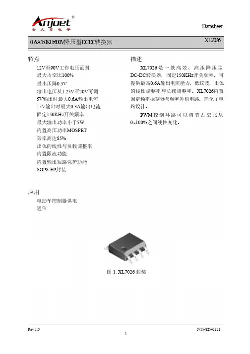
3A 52KHz 40V Buck DC to DC Converter XL2576特点:⏹宽输入电压范围3.6-40V⏹有3.3V,5V和可调版本⏹输出可调范围1.23V-38V⏹最大占空比100%⏹最小饱和压降1.3V⏹3A输出电流能力⏹内部优化功率管设计⏹效益高达90%⏹输出线性好且负载可调⏹TTL关断能力⏹内置频率补偿,软启动功能,热关断功能,限流功能短路保护功能⏹可选封装形式:TO-220,TO-263应用领域:⏹LCD监控器,LCD电视⏹数码像框⏹机顶盒⏹调制解调器⏹通信/网络设备概述XL2576是一个52KHz固定频率脉宽调制(降压型)DC/DC转换器。
高效率且高达3A负载驱动能力,低纹波,极好的线性和负载调节能力,仅需最少外部元。
可调输出使用简单,内建频率补偿和固定频率震荡器。
脉宽调制控制电路可以线性调节占空比从0到100%。
具有使能功能,内置过流和短路保护功能,当发生过流和短路保护时,XL2576工作频率从52KHz降到31KHz。
内置频率补偿模块使XL2576外部元件最少。
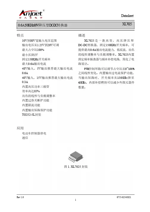
图1. XL2576封装类型3A 52KHz 40V Buck DC to DC Converter XL2576引脚设置图2. XL2576引脚结构(顶视图)表格1引脚描述引脚数引脚名描述1 输入电压输入引脚,XL2576工作在直流电压3.6V到40V,外接适合大的旁路电容到地来消除输入噪声。
2 输出功率开关输出引脚(SW).输出端是提供功率输出的开关结点。
3 GND 接地引脚,做版图时必须小心。
此引脚必须放置在硝特基二极管和输出电容到地的外面,来阻止电感电压噪声引起的开关电流毛刺输入到XL2576。
4 反馈反馈引脚(FB),通过外部电阻来分割回路,反馈是来检测和调节输出电压,反馈端电压是1.23V。
5 ON/OFF 使能引脚。
驱动ON/OFF 引脚为低电平则开启设备,驱动此引脚为高电平则关断设备,悬空默认为低电平。

基于LM2576的高可靠MCU电源设计-------------------------------------------------------------------------------------------摘要:在对线性稳压集成电路与开关稳压集成电路的应用特性进行比较的基础上,简单介绍了LM2576的特性,给出了基本开关稳压电源、工作模式可控的开关稳压电源和开关与线性结合式稳压电路的设计方案及元器件参数的计算方法。
关键词:LM2576电源设计MCU嵌入式控制系统的MCU一般都需要一个稳定的工作电压才能可靠工作。
而设计者多习惯采用线性稳压器件(如78xx系列三端稳压器件)作为电压调节和稳压器件来将较高的直流电压转变MCU所需的工作电压。
这种线性稳压电源的线性调整工作方式在工作中会大的“热损失”(其值为V压降×I负荷),其工作效率仅为30%~50%。
加之工作在高粉尘等恶劣环境下往往将嵌入式工业控制系统置于密闭容器内的聚集也加剧了MCU的恶劣工况,从而使嵌入式控制系统的稳定性能变得更差。
而开关电源调节器件则以完全导通或关断的方式工作。
因此,工作时要么是大电流流过低导通电压的开关管、要么是完全截止无电流流过。
因此,开关稳压电源的功耗极低,其平均工作效率可达70%~90%。
在相同电压降的条件下,开关电源调节器件与线性稳压器件相比具有少得多的“热损失”。
因此,开关稳压电源可大大减少散热片体积和PCB板的面积,甚至在大多数情况下不需要加装散热片,从而减少了对MCU工作环境的有害影响。
采用开关稳压电源来替代线性稳压电源作为MCU电源的另一个优势是:开关管的高频通断特性以及串联滤波电感的使用对来自于电源的高频干扰具有较强的抑制作用。
此外,由于开关稳压电源“热损失”的减少,设计时还可提高稳压电源的输入电压,这有助于提高交流电压抗跌落干扰的能力。
LM2576系列开关稳压集成电路是线性三端稳压器件(如78xx系列端稳压集成电路)的替代品,它具有可靠的工作性能、较高的工作效率和较强的输出电流驱动能力,从而为MCU的稳定、可靠工作提供了强有力的保证。

3.0 A, 15 V, Step-Down Switching RegulatorJM2576系列稳压器是单片集成电路,非常适合于降压开关稳压器(buck converter )的简便设计。
本系列电路均能驱动3.0A 负载,具有良好的线路和负载调节能力。
这些设备有3.3v 、5.0v 、12v 、15v 的固定输出电压和可调输出版本。
这些调节器的设计目的是尽量减少外部组件的数量,以简化电源设计。
几个不同的电感器制造商提供了与JM2576一起使用的标准系列电感器。
由于JM2576变换器是开关电源,其效率明显高于常用的三端线性稳压器,尤其是在输入电压较高的情况下。
在很多情况下功耗低,不需要散热器或者它的体积可以大大缩小。
一个标准系列的电感优化使用JM2576可从多个不同的制造商处获得。
这一特性大大简化了开关电源的设计。
JM2576的特点包括在规定的输入电压和输出负载条件下,输出电压的保证公差为±4%,振荡器频率的保证公差为±10%(在0°C 到125°C 之间为±2%)。
包括外部关机,具有80㎂(典型)备用电流。
输出开关包括逐周限流,以及故障条件下完全保护的热关机。
The JM2576 series of regulators are monolithic integrated circuits ideally suited for easy and convenient design of a step –down switching regulator (buck converter). All circuits of this series are capable of driving a 3.0 A load with excellent line and load regulation. These devices are available in fixed output voltages of 3.3 V, 5.0 V, 12 V, 15 V, and an adjustable output version.These regulators were designed to minimize the number of external components to simplify the power supply design. Standard series of inductors optimized for use with the JM2576 are offered by several different inductor manufacturers. Since the JM2576 converter is a switch – mode power supply, its efficiency is significantly higher in comparison with popular three –terminal linear regulators,especially with higher input voltages. In many cases, the power dissipated is so low that no heatsink is required or its size could be reduced dramatically.A standard series of inductors optimized for use with theJM2576 are available from several different manufacturers. This feature greatly simplifies the design of switch –mode power supplies. The JM2576 features include a guaranteed ±4% tolerance on output voltage within specified input voltages and output load conditions, and ±10% on the oscillator frequency (±2% over 0°C to 125°C). External shutdown is included, featuring 80 ㎂ (typical) standby current. The output switch includes cycle –by –cycle current limiting, as well as thermal shutdown for full protection under fault conditions.JM2576-xxTO-220-5LJM2576TTO-263-5LJM2576SPin connections1. Vin2. Output3. Ground4. Feedback5. ON/OFFFeatures ORDERING INFORMATION∙ 3.3 V, 5.0 V, 12 V, 15 V, and AdjustableOutput Versions∙ Adjustable Version Output Voltage Range,1.23 to 37 V ±4%∙ Maximum Over Line and Load Conditions∙Guaranteed 3.0 A Output Current∙Wide Input Voltage Range∙Requires Only 4 External Components∙52 kHz Fixed Frequency Internal Oscillator∙TTL Shutdown Capability, Low Power Standby Mode∙High Efficiency∙Uses Readily Available Standard Inductors∙Thermal Shutdown and Current Limit ProtectionApplications∙Simple High–Efficiency Step–Down (Buck) Regulator∙Efficient Pre–Regulator for Linear Regulators∙On–Card Switching Regulators∙Positive to Negative Converter (Buck–Boost)∙Negative Step–Up Converters∙Power Supply for Battery Chargers应用简单高效降压调节器用于线性调节器的高效预调节器卡上开关调节器正负转换器(降压-升压)负升压转换器电池充电器电源Typical Application (Fixed Output Voltage Versions)Figure 1.Representative Block Diagram and Typical ApplicationThis device contains 162 active transistors.Figure 2.ABSOLUTE MAXIMUM RATINGS(Absolute Maximum Ratings indicate limits beyond which damage to the device may occur.)≤ V ≤ +VinThese are stress ratings only and functional operation of the device at these or any other conditions beyond those indicated under “recommended operating conditions” is not implied.OPERATING RATINGS(Operating Ratings indicate conditions for which the device is intended to be functional, but do not guaranteespecific performance limits. For guaranteed specifications and test conditions, see the Electrical Characteristics.)SYSTEM PARAMETERS [Note 1]ELECTRICAL CHARACTERISTICS(Unless otherwise specified, V in = 12 V for the 3.3 V, 5.0 V, and Adjustable version, V in = 25 V for the 12 V version, and V in = 30 V for the 15 V version. I Load = 500 mA, T J = 25°C, for min/max values T J is the operating junction temperature range that applies [Note 2],unless otherwise noted.)≤Vin ≤ 40 V, 0.5 A I Load 3.0≤Vin ≤ 40 V, 0.5 A ILoad≤ 3.0 A)T J = 25°≤Vin ≤ 40 V, 0.5 A I Load 3.0≤Vin ≤ 40 V, 0.5 A I Load 3.0≤ Vin ≤ 40 V, 0.5 A I Load≤ 3.0 A, Vout = 5.0 V)T J = 25°1. External components such as the catch diode, inductor, input and output capacitors can affect switching regulator system performance.When the IL2576 is used as shown in the test circuit, system performance will be as shown in system parameters section .2. Tested junction temperature range for the IL2576: T low = –40°C T high = +125°CDEVICE PARAMETERSELECTRICAL CHARACTERISTICS(Unless otherwise specified, V in = 12 V for the 3.3 V, 5.0 V, and Adjustable version, V in = 25 Vfor the 12 V version, and V in = 30 V for the 15 V version. I Load = 500 mA, T J = 25°C, for min/max values T J is theoperating junction temperature range that applies [Note 2], unless otherwise noted.)3. The oscillator frequency reduces to approximately 18 kHz in the event of an output short or an overload which causes the regulated output voltage to drop approximately 40% from the nominal output voltage. This self protection feature lowers the average dissipation of the IC by lowering the minimum duty cycle from 5% down to approximately 2%.4. Output (Pin 2) sourcing current. No diode, inductor or capacitor connected to output pin.5. Feedback (Pin 4) removed from output and connected to 0 V.6. Feedback (Pin 4) removed from output and connected to +12 V for the Adjustable, 3.3 V, and 5.0 V versions, and +25 V for the 12 V and 15 V versions, to for ce the output transistor “off”.7. V in = 40 V.Fixed Output Voltage VersionsFigure 3. Cin – 100 mF, 75 V, Aluminium ElectrolyticCout – 1000 mF, 25 V, Aluminium ElectrolyticD1 – Schottky, MBR360L1 – 100 mH, Pulse Eng. PE–92108R1 – 2.0 k, 0.1%R2 – 6.12 k, 0.1%Adjustable Output Voltage VersionsFigure 4.⎛R⎫⎛V⎫V= V 1.0+2⎪,R = R out-1.0⎪Rout ref ⎪21V⎪⎝1⎭⎝ ref⎭Where Vref = 1.23 V, R1 between 1.0 k and 5.0 kC1= 10 nFC2= 1 nFApplication InformationINVERTING REGULATORFigure 5 shows a JM2576-12 in a buck-boost configuration to generate a negative 12V output from a positive input voltage. This circuit bootstraps the regulator’s ground pin to the negative output voltage, then by grounding the feedback pi n, the regulator senses the invert ed output voltage and regulates it to −12V.For an input voltage of 12V or more, the maximum available output current in this configuration is approximately 700 mA. At lighter loads, the minimum input voltage required drops to approximately 4.7V.The switch currents in this buck-boost configuration are higher than in the standard buck-mode design, thus lowering the available output current. Also, the start-up input current of the buck-boost converter is higher than the standard buck-mode regulator, and this may overload an input power source with a current limit less than 5A. Using a delayed turn-on or an undervoltage lockout circuit (described in the next section) would allow the input voltage to rise to a high enough level before the switcher would be allowed to turn on.Because of the structural differences between the buck and the buck-boost regulator topologies, the buck regulator design procedure section can not be used to to select the inductor or the output capacitor. The recommended range of inductor values for the buck-boost design is between 68 µH and 220 µH, and the output capacitor values must be larger than what is normally required for buck designs. Low input voltages or high output currents require a large value output capacitor (in the thousands of micro Farads).The peak inductor current, which is the same as the peak switch current, can be calculated from the following formula:Where f osc = 52 kHz. Under normal continuous inductor current operating conditions, the minimum V IN representsthe worst case. Select an inductor that is rated for the peak current anticipated.FIGURE 5. Inverting Buck-Boost Develops −12VAlso, the maximum voltage appearing across the regulator is the absolute sum of the input and output voltage. For a −12V output, the maximum input voltage for the JM2576 is +28V.应用程序信息逆变调节器图5显示了一个buck-boost配置中的JM2576-12,它从正输入产生负12V输出电压。


页数:第1 页,共3 页描述221015A02是为产品XL2576制作的演示板,用于DC8V~40V输入,输出电压5V,输出电流3A的降压恒压应用演示,最高转换效率可以达到86%。
XL2576是开关降压型DC-DC转换芯片;固定开关频率52KHz,可减小外部元器件尺寸,方便EMC设计。
芯片具有出色的线性调整率与负载调整率,输出电压支持1.23V~37V间任意调节。
芯片内部集成过流保护、过温保护、短路保护等可靠性模块。
XL2576为标准TO263-5L封装,集成度高,外围器件少,应用灵活。
DEMO原理图引脚介绍页 数:第 2 页, 共 3 页物料清单序号 数量 参考位号 说明生产商型号 生产商 1 2 C1,C2 1uF,50V,Ceramic,X7R,0805 C2012X7R1H105K TDK 2 1 CFF 33nF,50V,Ceramic,X7R,0603 C1608X7R1H333K TDK 3 2 CIN, COUT220uF,50V,Electrolytic,(10*16) YXJ-50V-220uFRubycon 4 1 D1 60V,5A,SMC,Schottky Barrier RectifierB560CDIODES5 1 L1 100uH,4A,(18*9)6 1 R1 14K Ω,1%,1/16W,Thick Film,0603 RC0603FR-0714KL Yageo7 1 R2 43K Ω,1%,1/16W,Thick Film,0603RC0603FR-0743KLYageo 81U140V,3A,BUCK,DC-DC Converter,TO263-5LXL2576XLSEMIDEMO 实物图PCB 布局40mm顶层 底层30mm页数:第3 页,共3 页应用信息输入电容选择在连续模式中,转换器的输入电流是一组占空比约为VOUT/VIN的方波。
为了防止大的瞬态电压,必须采用针对最大RMS电流要求而选择低ESR(等效串联电阻)输入电容器。
LM2576详细介绍LM2576是一款专为电源应用而设计的高效率降压稳压芯片。
它采用了功率MOSFET开关和专业设计的控制电路,能够以固定频率的方式实现恒压或恒流输出。
LM2576通过非常简单的外围器件就可以完成稳压电源设计,无需繁琐的调整和复杂的电路设计。
1.高效率:LM2576采用了开关式降压稳压的原理,相比传统的线性稳压芯片,具有更高的转换效率。
在负载较低的情况下,也能保持高效率。
2.宽输入电压范围:LM2576的输入电压范围从4V至40V,可以适应不同的电源输入条件。
3.固定输出电压:LM2576有多种型号可供选择,每种型号都有固定的输出电压。
用户可以根据需求选择不同的型号,无需调节电路即可得到所需的输出电压。
4.输出电流高:LM2576能够提供高达3A的输出电流,适用于大多数低压电源应用。
5.低输出噪声:LM2576采用了片内反馈调节电路,能够有效地抑制输出噪声。
此外,它还具有过温保护和短路保护功能,能够保证电路的可靠性和安全性。
6.简单的外围器件:LM2576的外围器件非常简单,只需一颗电容和一个电感即可实现稳压功能。
这样就减少了外围元件的数量和尺寸,可以大大减小整个电源的体积。
7.应用广泛:由于LM2576具有高效率、稳定可靠的特点,被广泛应用于工业控制、通信设备、汽车电子、电子游戏机等领域。
总结起来,LM2576是一款高效、稳定、可靠的降压稳压芯片,具有固定输出电压、宽输入电压范围和高输出电流等优点。
它适用于各种低压电源应用,可以简化电路设计,降低系统成本,提高电源的效率和可靠性。
IL2576HV/LM2576HV系列稳压器是单片集成电路,为降压型开关稳压器提供所有有源功能,能够以出色的线路和负载调节来驱动3A负载。
这些设备提供3.3 V,5 V,12 V,15 V的固定输出电压,以及可调输出版本。
这些稳压器需要最少的外部组件,易于使用,并包括故障保护和固定频率振荡器。
IL2576HV/LM2576HV系列可为流行的三端线性稳压器提供高效替代。
它大大减小了散热器的尺寸,并且在某些情况下不需要散热器。
几个不同的制造商都提供了针对IL2576HV/LM2576HV系列使用而优化的标准系列电感器。
此功能极大地简化了开关电源的设计。
其他功能包括在规定的输入电压和输出负载条件下,输出电压的容差为±4%,在振荡器频率上的容差为±10%。
包括外部关机功能,待机电流典型值为50 µA。
输出开关包括逐周期限流以及热关断功能,可在故障情况下提供全面保护。
IL2576HV LM2576HVR-12 LM2576HVSX-12 LM2576HVS-ADJ LM2576HVR-12 LM2576HVT1Features•LMR33630 36V,3A,400kHz同步转换器• 3.3V,5V,12V,15V和可调输出版本•可调版本输出电压范围:1.23 V至37 V(对于HV 版本为57 V)在整个线路和负载条件下最大±4%•指定的3A输出电流•宽输入电压范围:40 V,最高为HV 60 V•仅需四个外部组件•52kHz固定频率内部振荡器•TTL关机功能,低功耗待机模式•高效率•使用现成的标准电感器•热关断和限流保护•使用WEBENCH工具创建自定义设计2Applications•马达驱动•商家网络和服务器PSU•家电类•测试测量设备3DescriptionLM2576HVR-12 LM2576HVSX-12 LM2576HVS-ADJ LM2576HVR-12 LM2576HVT稳压器是单片集成电路,为降压型开关稳压器提供所有有源功能,能够以出色的线路和负载调节来驱动3A负载。
n LCD Monitor and LCD TVn Portable instrument power supply n Telecom / Networking Equipmentcomponent count.Figure1. Package Type of XL4015Pin ConfigurationsFigure2. Pin Configuration of XL4015 (Top View)Table 1 Pin DescriptionPin NumberPin Name Description1GNDGround Pin. Care must be taken in layout. This pin should be placed outside of the Schottky Diode to output capacitor ground path to prevent switching current spikes from inducing voltage noise into XL4015.2 FB Feedback Pin (FB). Through an external resistor divider network, FB senses the output voltage and regulates it. The feedback threshold voltage is 1.25V .3 SW Power Switch Output Pin (SW). SW is the switch node that supplies power to the output.4 VC Internal V oltage Regulator Bypass Capacity. In typical system application, The VC pin connect a 1uf capacity to VIN.5 VINSupply V oltage Input Pin. XL4015 operates from a 8V to 36V DC voltage. Bypass Vin to GND with a suitably large capacitor to eliminate noise on the input.Function BlockFigure3. Function Block Diagram of XL4015Typical Application CircuitFigure4. XL4015 Typical Application Circuit (VIN=8V~36V, VOUT=5V/5A)Order Information Marking ID Package Type Packing Type Supplied AsXL4015E1 XL4015E1 TO263-5L 800 Units on Tape & Reel XLSEMI Pb-free products, as designated with “E1” suffix in the par number, are RoHS compliant.Absolute Maximum Ratings(Note1)Parameter Symbol Value Unit Input Voltage Vin -0.3 to 40 V Feedback Pin Voltage V FB-0.3 to Vin V Output Switch Pin Voltage V Output-0.3 to Vin V Power Dissipation P D Internally limited mW Thermal Resistance (TO263-5L)R JA30 ºC/W (Junction to Ambient, No Heatsink, Free Air)Operating Junction Temperature T J-40 to 125 ºC Storage Temperature T STG-65 to 150 ºC Lead Temperature (Soldering, 10 sec) T LEAD260 ºC ESD (HBM) >2000 V Note1: Stresses greater than those listed under Maximum Ratings may cause permanent damage to the device. This is a stress rating only and functional operation of the device at these or any other conditions above those indicated in the operation is not implied. Exposure to absolute maximum rating conditions for extended periods may affect reliability.XL4015 Electrical CharacteristicsT a = 25℃;unless otherwise specified.Symbol Parameter Test Condition Min. Typ. Max. Unit System parameters test circuit figure4VFB FeedbackV oltageVin = 8V to 40V, V out=5VIload=0.5A to 5A1.225 1.25 1.275 VEfficiency ŋVin=12V ,V out=5VIout=5A- 87 - %Efficiency ŋVin=24V ,V out=12VIout=4A- 93 - %Electrical Characteristics (DC Parameters)Vin = 12V, GND=0V, Vin & GND parallel connect a 220uf/50V capacitor; Iout=500mA, T a = 25℃; the others floating unless otherwise specified.Parameters Symbol Test Condition Min. Typ. Max. Unit Input operation voltage Vin 8 36 V Quiescent Supply Current I q V FB =Vin 2.1 5 mA Oscillator Frequency Fosc 144 180 216 KHz Output Short Frequency Fosp 48 KHz Switch Current Limit I L V FB =0 7 A Max. Duty Cycle D MAX V FB=0V 100 %Output Power PMOS Rdson V FB=0V, Vin=12V,I SW=5A60 80 mohmTypical System Application (VOUT=5V/5A)Efficiency VS Output currentFigure6. XL4015 System Efficiency CurveTypical System Application (VOUT=12V/4A)Efficiency VS Output currentFigure8. XL4015 System Efficiency CurveLogic level signals shutdown function can be used in typical system application with external components. When the TTL high voltage above 3.3V(referenced to ground, lower than VIN), the converter will shutdown, input current less than 5mA; when the TTL Low voltage below0.8V(referenced to ground), the converter will turn on.Figure9. XL4015 Typical Application CircuitPackage Information TO263-5L。
n Built in Thermal Shutdown Function n Built in Current Limit Function n Available in SOIC-8 packageApplicationsn Automotive and Industrial Boost /Buck-Boost / Inverting Converters n Portable Electronic EquipmentFigure1. Package Type of XL6007Pin Configurations SWSWFigure2. Pin Configuration of XL6007 (Top View)Table 1 Pin DescriptionPin NumberPin Name Description1 ENEnable Pin. Drive EN pin low to turn off the device, drive ithigh to turn it on. Floating is default high.2 VINSupply V oltage Input Pin. XL6007 operates from a 3.6V to 24V DC voltage. Bypass Vin to GND with a suitably large capacitor to eliminate noise on the input.3 FB Feedback Pin (FB). The feedback threshold voltage is 1.25V .4 NC No Connected.5,6 SWPower Switch Output Pin (SW). Output is the switch node thatsupplies power to the output.7,8 GND Ground Pin.Function BlockFigure3. Function Block Diagram of XL6007 Typical Application CircuitFigure4. XL6007 Typical Application Circuit (Boost Converter)to the device. This is a stress rating only and functional operation of the device at these or any other conditions above those indicated in the operation is not implied. Exposure to absolute maximum rating conditions for extended periods may affect reliability.XL6007 Electrical CharacteristicsT a = 25℃;unless otherwise specified.Symbol Parameter Test Condition Min. Typ. Max. Unit System parameters test circuit figure4VFB FeedbackV oltageVin = 12V to 16V, V out=18VIload=0.1A to 0.5A1.213 1.25 1.287 VEfficiency ŋVin=12V ,V out=18.5VIout=0.5A- 90 - %Electrical Characteristics (DC Parameters)Vin = 12V, GND=0V, Vin & GND parallel connect a 220uf/50V capacitor; Iout=0.5A, T a = 25℃; the others floating unless otherwise specified.Parameters Symbol Test Condition Min. Typ. Max. Unit Input operation voltage Vin 3.6 24 V Shutdown Supply Current I STBY V EN=0V 70 100 uAQuiescent Supply Current I q V EN =2V,V FB =Vin2.5 5 mAOscillator Frequency Fosc 320 400 480 Khz Switch Current Limit I L V FB =0 2 AOutput Power NMOS Rdson Vin=12V,I SW=2A110 120 mohmEN Pin Threshold V EN High (Regulator ON)Low (Regulator OFF)1.40.8VI H V EN =2V (ON) 3 10 uA EN Pin Input LeakageCurrent ILV EN =0V (OFF) 3 10 uA Max. Duty Cycle D MAX V FB=0V 90 %Typical System Application – Boost (Output 18.5V/0.5A)Figure5. XL6007 Typical System Application (Boost Converter)Typical System Application – SEPIC Buck-Boost (Input 10V~18V , Output 12V/0.5A)Figure6. XL6007 Typical System Application (SEPIC Buck-Boost Converter)Typical System Application for Inverting Converter– SEPIC Inverting Topology (Input 10V~18V , Output + -12V/0.6A)Figure7. XL6007 Typical System Application (SEPIC Inverting Converter)Package InformationSOP8 Package Mechanical Dimensions。
3A正压转负压电路.ddb
主要是为把+5V电压转换出一个-5V电压用
采用 LM2576-ADJ 3A输出可调电源芯片制作,开关频率50KHZ
该电路的典型应用是降压,因为是斩波式降压,所以效率比较高能达到80%
输入电压5V~40V,输出1.2V~37V
代替DCDC模块和7805等效果都不错
3A正压转负压电路
输入电压4.5V~30V 输出-1.25~-25V 最大电流可接近3A,静态电流10mA~20mA
可以用于需要负电源的场合
成本较低 LM2576-ADJ为1.5元/片
LM2575为最大电流1A的芯片,可以直接替换
LM2595,LM2596开关频率150KHZ,需要的电感能小一些,但开关损耗可能就大一些,引脚都一样
如果购买,可能会遇到假货,LM2575直插假货和LM2596贴片假货都遇到过
LM2576质量还不错,直插贴片都正常
这张图比较小,大图看rar的protel文件,原理带着解释。