XL4015降压型直流电源变换器芯片(大功率型)
- 格式:pdf
- 大小:283.05 KB
- 文档页数:10
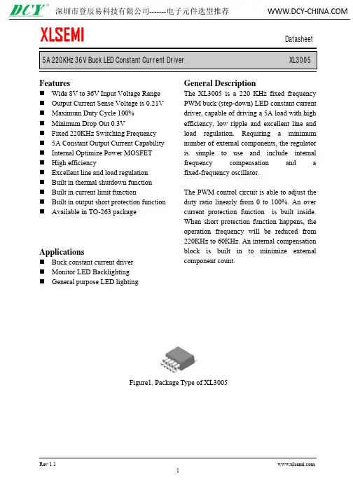
5A 220KHz 36V Buck LED Constant Current Driver XL3005FeaturesWide 8V to 36V Input Voltage Range Output Current Sense Voltage is 0.21V Maximum Duty Cycle 100% Minimum Drop Out 0.3VFixed 220KHz Switching Frequency 5A Constant Output Current Capability Internal Optimize Power MOSFET High efficiencyExcellent line and load regulation Built in thermal shutdown function Built in current limit functionBuilt in output short protection function Available in TO-263 packageApplicationsBuck constant current driver Monitor LED Backlighting General purpose LED lightingGeneral DescriptionThe XL3005 is a 220 KHz fixed frequency PWM buck (step-down) LED constant current driver, capable of driving a 5A load with high efficiency, low ripple and excellent line and load regulation. Requiring a minimum number of external components, the regulator is simple to use and include internal frequency compensation and a fixed-frequency oscillator.The PWM control circuit is able to adjust the duty ratio linearly from 0 to 100%. An over current protection function is built inside. When short protection function happens, the operation frequency will be reduced from 220KHz to 60KHz. An internal compensation block is built in to minimize external component count.Figure1. Package Type of XL30055A 220KHz 36V Buck LED Constant Current Driver XL30055A 220KHz 36V Buck LED Constant Current Driver XL3005Figure4. XL3005 Typical Application Circuit5A 220KHz 36V Buck LED Constant Current Driver XL30055A 220KHz 36V Buck LED Constant Current Driver XL30055A 220KHz 36V Buck LED Constant Current Driver XL30055A 220KHz 36V Buck LED Constant Current Driver XL30055A 220KHz 36V Buck LED Constant Current Driver XL3005 Figure13. XL3005 System Parameters Test Circuit (VIN=8V~36V, IOUT=308mA)5A 220KHz 36V Buck LED Constant Current Driver XL3005 Figure15. XL3005 System Parameters Test Circuit (VIN=8V~36V, IOUT=615mA)5A 220KHz 36V Buck LED Constant Current Driver XL3005 Figure17. XL3005 System Parameters Test Circuit (VIN=8V~36V, IOUT=925mA)5A 220KHz 36V Buck LED Constant Current Driver XL3005 Figure19. XL3005 System Parameters Test Circuit (VIN=8V~36V, IOUT=1540mA)5A 220KHz 36V Buck LED Constant Current Driver XL3005 Figure21. XL3005 System Parameters Test Circuit (VIN=8V~36V, IOUT=2140mA)5A 220KHz 36V Buck LED Constant Current Driver XL3005Figure23. XL3005 System Parameters Test Circuit (PWM DIMMING)Typical System Application (LED OVP)be limited in a suitable value by choose different zener diode when the output LED open. the zener diode Figure24. XL3005 System Parameters Test Circuit (LED OVP)5A 220KHz 36V Buck LED Constant Current Driver XL30055A 220KHz 36V Buck LED Constant Current Driver XL3005 Important NoticeXLSEMI reserve the right to make modifications, enhancements, improvements, corrections or other changes without notice at any time. XLSEMI does not assume any liability arising out of the application or use of any product described herein; neither does it convey any license under its patent rights, nor the rights of others. XLSEMI assumes no liability for applications assistance or the design of Buyers’ products. Buyers are responsible for their products and applications using XLSEMI components. To minimize the risks associated with Buyers’ products and applications, Buyers should provide adequate design and operating safeguards. XLSEMI warrants performance of its products to the specifications applicable at the time of sale, in accordance with the warranty in XLSEMI’s terms and conditions of sale of semiconductor products. Testing and other quality control techniques are used to the extent XLSEMI deems necessary to support this warranty. Except where mandated by applicable law, testing of all parameters of each component is not necessarily performed.For the latest product information, go to .。
零电压反激式开关电源芯片IRIS4015原理及设计要点摘要:本文介绍了准谐式反激式开关电源IRIS4015的工作原理,并介绍了应用IRIS4015进行电源设计的电路和在设计中应特别注意的几个方面。
叙词:谐振Abstract: The principle of quasi-resonance fly-back SMPS IRIS4015 was in troduced in this paper, and the application circuit of the IRIS4015 in th e design of the SMPS and the design note were also introduced. Keywords:Quasi-Resonance 1. 引言目前单片开关稳压电源有多种多样,如TOP-switch、Tiny-switch、Cool-set等,这些单片开关稳压电源均工作在硬开关状态,开关损耗和EMI较大。
为克服硬开关的缺点可用软开关工作方式。
在反激式开关电源中以无损耗缓冲电路和准谐振工作方式最为简单,而且准谐振工作方式可以实现零电压的开通和关断,在各种准谐振的解决方案中IRIS4015是一种很好的方案。
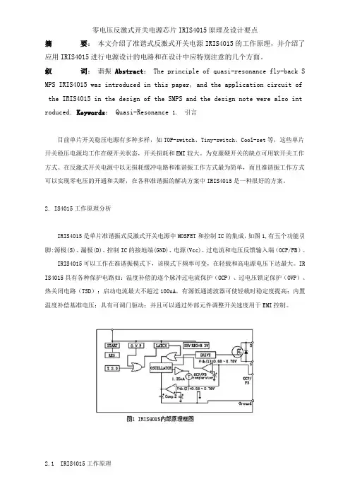
2. IS4015工作原理分析IRIS4015是单片准谐振式反激式开关电源中MOSFET和控制IC的集成,如图1,有五个功能引脚:源极(S)、漏极(D)、控制IC的接地端(GND)、电源(Vcc)、过电流和电压反馈输入端(OCP/FB)。
IRIS4015可以工作在准谐振模式下,该模式下频率可变,在轻载和高电源电压下达最大。
IR IS4015具有各种保护电路如:温度补偿的逐个脉冲过电流保护(OCP)、过电压锁定保护(OVP)、热关闭电路(TSD);启动电流最大不超过100uA,有源低通滤波器可使轻载时稳定度提高;内置温度补偿基准电压;具有可调门驱动;并且可以通过外部元件调整开关速度用于EMI控制。
• 177•池、燃料电池等,其中前两种为传统电源,比能量低、维护不便;燃料电池为新兴能源,比能量高、但技术不成熟;当前无人机主流电源为锂电子电池,其具有比能量高等优点。
此系统选用锂电子动力电池松下NCR18650PF ,电压3.7v 内阻25m Ω以内,容量2900mA 质量47克放电电流10A 。
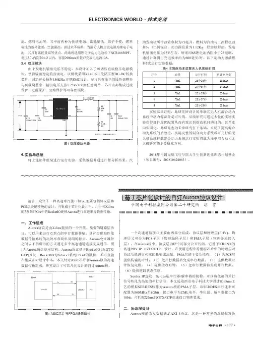
3.4 稳压模块由于发电机输出电压不稳定,本设计加入了可调压直流稳压电源模块,使得输出稳定的直流电。
该模块采用XL4015开关降压型DC-DC 转换芯片,固定开关频率180KHz,方便EMC 设计。
芯片具有出色的线性调整率与负载调整率,输出电压支持1.25V-32V 间任意调节。
芯片内部集成过流保护、过温保护、短路保护等可靠性模块。
图1 稳压模块电路4.实验与总结将上述部件组装进行运行实验,采集数据并通过计算分析结果,汽油发动机所带油箱容积为75毫升,燃料为汽油与二冲程机油按5:1比例混合,动力源总重为1.12Kg ,经实验得出,发电机输出电压为15V 左右,所采用6S 锂电池内阻小于25毫欧,通过计算得出充电效率约为600毫安/时。
以下是动力源满燃料5次运行实验数据:表4 主流航拍多旋翼无人机续航时间序号油量运行时间估计充电量175ml 23分10秒232mAh 275ml 24分07秒241mAh 375ml 22分35秒226mAh 475ml 23分37秒236mAh 575ml23分15秒233mAh实验结果证明,此研究所设计的串联式无人机混合动力系统中动力源部分是可行的,后续研究可通过大量的实物实验获得部件最优配置从而有效达到提高航时的目的,甚至走向实用化。
此研究也为未来研究打下基础,点明了提高混合动力系统的质效比,实施完整的混合动力系统或可飞行的无人机系统挂载混合动力系统运行实验将成为油电混合动力无人机研究的主要研究方向。
2018年中国民航飞行学院大学生创新创业训练计划基金(项目编号:201810624063)。
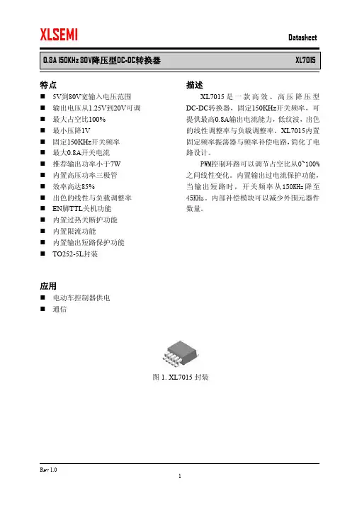
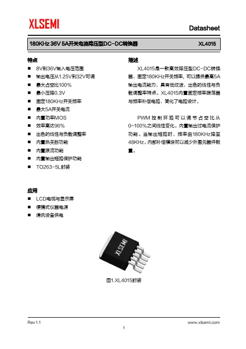
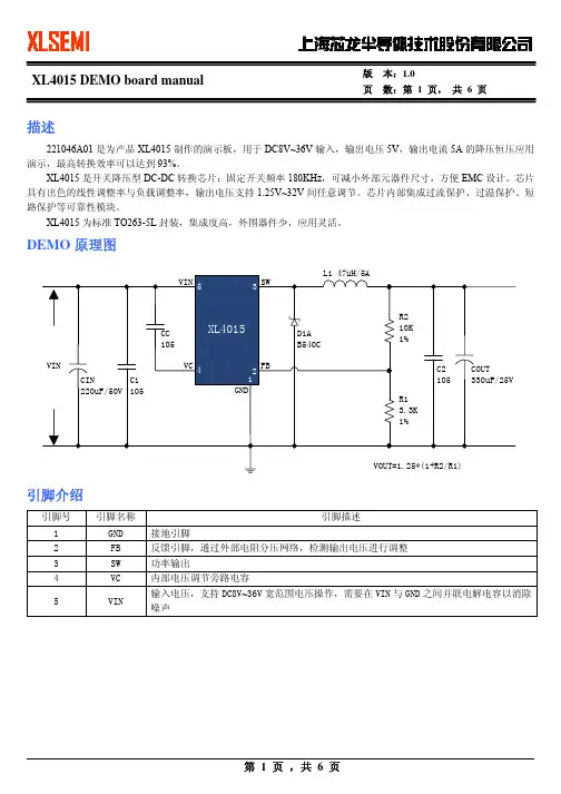
180KHz 36V 5A 开关电流降压型DC-DC转换器XL4015特点⏹8V到36V输入电压范围⏹输出电压从1.25V到32V可调⏹最大占空比100%⏹最小压降0.3V⏹固定180KHz开关频率⏹最大5A开关电流⏹内置功率MOS⏹效率高达96%⏹出色的线性与负载调整率⏹内置热关断功能⏹内置限流功能⏹内置输出短路保护功能⏹TO263-5L封装应用⏹LCD电视与显示屏⏹便携式仪器电源⏹通讯设备供电描述XL4015是一款高效降压型DC-DC转换器,固定180KHz开关频率, 可以提供最高5A输出电流能力,具有低纹波,出色的线性与负载调整率特点。
XL4015内置固定频率振荡器与频率补偿电路,简化了电路设计。
PWM控制环路可以调节占空比从0~100%之间线性变化。
内置输出过电流保护功能。
当输出短路时,频率由180KHz降至48KHz。
内部补偿模块可以减少外围元器件数量。
图1.XL4015封装180KHz 36V 5A 开关电流降压型DC-DC 转换器 XL4015引脚配置VIN SW FB GNDVC 12345TO263-5LMetal Tab SW图2. XL4015引脚配置表1.引脚说明引脚号 引脚名称 描述1 GND 接地引脚。
2 FB 反馈引脚,通过外部电阻分压网络,检测输出电压进行调整,参考电压为1.25V 。
3 SW 功率开关输出引脚,SW 是输出功率的开关节点。
4 VC 内部电压调节器旁路电容引脚,需要在VIN 与VC 引脚之间连接1个1uF 电容。
5 VIN电源输入引脚,支持DC8V~36V 宽范围电压操作,需要在VIN 与GND 之间并联电解电容以消除噪声。
180KHz 36V 5A 开关电流降压型DC-DC 转换器 XL4015方框图EAGNDFB3.3V1.25VEA COMPOscillator180KHz/48KHz3.3V Regulator1.25V Reference Start UpLatchCOMP2COMP1DriverThermal ShutdownVINVCSW220mV 200mV28m ΩCurrent LimitPower PMOS1:100020K Ω3.3nFOSP图3. XL4015方框图典型应用XL4015CIN220uF/50VCOUT330uF/25VR210KR13.3KD1MBRD1045GC1105C21055312VIN4VOUT=1.25*(1+R2/R1)VIN VCSWGNDFBCC 105CFF 33nFVOUT图4. XL4015系统参数测量电路 (VIN=8V~36V, VOUT=5V/5A)180KHz 36V 5A开关电流降压型DC-DC转换器XL4015订购信息产品型号打印名称封装方式包装类型XL4015E1 XL4015E1 TO263-5L 800只每卷XLSEMI无铅产品,产品型号带有“E1”后缀的符合RoHS标准。
基于STM32的多路OLED驱动电源系统设计王菲;赵彦【摘要】针对OLED测试的驱动电源功能单一的问题,介绍一种基于STM32的多功能OLED驱动电源系统.系统以STM32为核心,通过手动调节或者上位机软件方式设置参数后,控制DA芯片采取电流负反馈的方式控制XL4015的输出电压或者电流值,实现对4通道的OLED的恒压,恒流,占空比及频率可调,电压-电流混合源四种驱动方式,同时可以根据OLED样品测试要求选择不同的输出通道.实验测试结果研究表明,系统不仅误差小,分辨率高,稳定性好,纹波系数小,而且操作简单,可以实现多路OLED的实时数据显示和控制,具有良好的工程实用价值.【期刊名称】《电子测试》【年(卷),期】2019(000)010【总页数】3页(P22-24)【关键词】OLED;STM32;驱动电源;电压-电流混合源【作者】王菲;赵彦【作者单位】西安交通工程学院,陕西西安,710300;西安交通工程学院,陕西西安,710300【正文语种】中文0 引言随着数字高清产品、多媒体终端的日益增长,基于有机发光器件OLED的平板显示技术开始受到广泛的关注。
相比传统的显示器件,基于OLED器件的显示技术具有视角广,响应速度快、省电、耐低温,抗震性好等的优点[1-2]。
但是,目前还面临着发光性能,稳定性,寿命等问题,因此需要针对OLED的寿命,发光性能等进行测试来综合评价器件的性能[3-4]。
由于OLED器件的发光亮度和驱动的电流成正比,一般采用恒流或者电压特性驱动OLED,目前OLED驱动电源按主要分为电压源驱动,交流驱动;按照驱动模式,可以分为有源阵列驱动和无源阵列驱动[5-6]。
目前,基于OLED的驱动电源主要采用51系列单片机,虽然简单,但是在数据的传输响应速度慢,测试效率低,与51单片机相比,基于STM32的OLED电源驱动系统更适合完成测试OLED的驱动电源。
根据目前的研究,本文设计了一种基于STM32可调可控的多通道OLED驱动电源,不仅可以能够灵活的设置OLED驱动所需的四种模式的电源,还可以通过上位机软件调节控制。
xl4015e工作原理XL4015E是一种非同步降压转换器,也称为buck转换器。
它通过降低输入电压以产生输出电压,以满足不同电路和设备的电源需求。
这种转换器广泛应用于各种电子设备中,如电子照明、电源适配器、车载电源等。
XL4015E的工作原理如下:1.输入电压:XL4015E可以接受范围在4.5V至32V之间的输入电压。
这些电压通常来自电池或其他电源。
2.电感:XL4015E中的一个重要组成部分是电感器。
电感器是由线圈组成的电子元件,当电流通过线圈时,会在线圈周围产生磁场。
这个磁场可以存储磁能量。
3.开关管:XL4015E中还包含一个开关管,用于控制电路的开关状态。
当开关管导通时,电感器开始充电;当开关管关闭时,电感器开始放电。
4.复合开关管:XL4015E同时还配备了一个复合开关管,用于实现高速开关和调节输出电压。
5.输出电压控制:通过控制开关管的开关频率和开关时间,可以调节电感器的充电和放电速率,从而控制输出电压的稳定性和精确度。
6.反馈控制:XL4015E还配备了一个反馈电路,用于监测和调节输出电压。
反馈电路将输出电压与设定的目标电压进行比较,并调整开关管的工作状态以实现输出电压的稳定。
7.过载保护:XL4015E还具有过载保护功能,当输出电流超过预设范围时,转换器会自动关闭以避免损坏。
总体上,XL4015E的工作原理就是通过将输入电压通过开关管和电感器进行荷电和放电来实现输出电压的稳定和调节。
通过控制开关管和反馈电路,可以提供稳定和可调节的输出电压,以满足各种电路和设备的需求。
以上是关于XL4015E工作原理的基本介绍,希望能对您有所帮助。
XL4015 5A 降压型直流电源变换器芯片(大功率型 )XL4015 5A 降压型直流电源变换器芯片(大功率型 ) 产品名称: XL4015 5A 降压型直流电源变换器芯片(大功率型 ) 产品型号: XL4015 产品展商:深圳劲锐佳科技有限公司产品文档:无相关文档简单介绍 XL4015 5A 降压型直流电源变换器芯片 (大功率型 ) 1、最大输出电流:5A ;2、最高输入电压: XL4015 为 8~36V 3 、输出电压: ADJ (0.8V) 可调; 4、振动频率: 180kHz ;5、转换效率: 85%~ 95%(不同电压输出时的效率不同);6、控制方式: PWM ;7、工作温度范围: -40℃~ +125℃ 8、工作模式:低功耗/正常两种模式可外部控制; XL4015 5A 降压型直流电源变换器芯片 (大功率型 )1、最大输出电流: 5A ;2、最高输入电压: XL4015 为8~36V3 、输出电压: ADJ (0.8V) 可调;4、振动频率:160kHz ;5、转换效率: 85%~ 95%(不同电压输出时的效率不同);6、控制方式: PWM ; 7、工作温度范围: -40℃~+125℃ 8、工作模式:低功耗 /正常两种模式可外部控制; 9、工作模式控制: TTL 电平兼容; 10、所需外部元件:只需极少的外围器件便可构成高效稳压电路;外围元件少,低纹波。
输入 25V电压,输出 12V 情况下,效率可达到 95%。
12、器件保护:热关断及电流限 ,输出短路保护功能;输入电源开关噪声抑制功能;Enanle 开关信号的迟滞功能;技术特点 (功能兼容 )---AOZ1014,LM2677,LM2678,LM2679 (1)全内置型单片高电压、高频率、高效率、大电流、高可靠性、高性价比集成电路;(2)系统设计简单、方便灵活、高功率密度;( 3)常规的过流保护,过热保护,输出短路保护都内置;(4)高效率,在输入电压 20V-30V ,输出功率 50W 时效率高达90%以上。
XL7015降压型直流电源变换器芯⽚(⾼电压型)DatasheetXL7015 0.8A150KHz80V降压型DC-DC转换器特点描述5V到80V宽输⼊电压范围输出电压从1.25V到20V可调?最⼤占空⽐100%XL7015是⼀款⾼效、⾼压降压型DC-DC转换器,固定150KHz开关频率,可提供最⾼0.8A输出电流能⼒,低纹波,出⾊的线性调整率与负载调整率。
XL7015内置固定频率振荡器与频率补偿电路,简化了电路设计。
最⼩压降1V固定150KHz开关频率?最⼤0.8A输出电流48V输⼊、5V输出推荐最⼤输出电流0.6APWM控制环路可以调节占空⽐从0~100%之间线性变化。
内置输出过电流保护功能,当输出短路时,开关频率从150KHz降⾄45KHz。
内部补偿模块可以减少外围元器件数量。
48V输⼊、15V输出推荐最⼤输出电流0.4A内置⾼压功率三极管效率⾼达85%出⾊的线性与负载调整率EN脚TTL关机功能内置过热关断护功能内置限流功能内置输出短路保护功能TO252-5L封装应⽤电动车控制器供电通信图1.XL7015封装XL7015 0.8A150KHz80V降压型DC-DC转换器引脚配置图2.XL7015引脚配置引脚号1引脚名描述电源输⼊引脚,⽀持DC5V~80V范围电压输⼊,需要在VIN与GND之间并联电解电容以消除噪声。
VIN2 3SW功率开关输出引脚,SW是输出功率的开关节点。
接地引脚。
GND反馈引脚,通过外部电阻分压⽹络,检测输出电压进⾏调整。
参考电压为1.25V。
4 5FBEN使能引脚,低电平⼯作,⾼电平关机,悬空时为低电平。
XL7015 0.8A150KHz80V降压型DC-DC转换器⽅框图图3.XL7015⽅框图典型应⽤图4.XL7015系统参数测量电路XL7015E1TO252-5L2500只每卷XLSEMI ⽆铅产品,产品型号带有“E1”后缀的符合RoHS 标准。
绝对最⼤额定值(注1)参数符号值单位V 输⼊电压-0.3to 85-0.3to Vin -0.3to Vin 内部限制Vin 反馈引脚电压输出开关引脚电压功耗V V FB V Output P D V mW 热阻(TO252-5L)R JA 50oC/W (结到环境,⽆外部散热⽚)最⼤结温-40到150-40到125-65到150260oC oC oC oC V引脚温度(焊接10秒)ESD (⼈体模型)T LEAD>3000Note1:超过绝对最⼤额定值可能导致芯⽚永久性损坏,在上述或者其他未标明的条件下只做功能操作,在绝对最⼤额定值条件下长时间⼯作可能会影响芯⽚的寿命。
锂电池供电的高效、低纹波、低高频噪声电源设计作者:陈昕来源:《电子技术与软件工程》2015年第16期摘要设计了一种锂电池供电的非隔离多路直流电源,嵌入到便携式移动设备中,电源有两路功率较大,效率、纹波、高频噪声的要求高。
存在锂电池输出电压低时与电源输出电压较接近,普通的降压DC/DC难以实现的问题,设计采用了超低压差、占空比可达100%、高效率的BUCK变换器,解决了该问题。
其中一路要求输出电压大范围可调、纹波小于1mV;设计采用了BUCK加LDO电路进行稳压,又明显减小了电源纹波;还用减法放大器控制BUCK电路,保持LDO的工作压差是较小的固定值,保证了电源的高效率。
电源又增加了LC滤波和磁珠滤波,对进一步减小纹波和高频噪声的效果较好。
【关键词】BUCK LDO 纹波滤波锂电池因容量大、体积小、无记忆效应、电量检测容易、使用寿命长等许多优点,并且产品种类多,技术成熟,在许多移动设备、车辆中得到了广泛的使用。
非隔离的开关电源技术也非常成熟,具有体积小、效率高、芯片种类多等优点,很广泛地应用在各个领域中。
在某科研课题中,需要使用锂电池为便携式小体积设备提供多路直流电源,其中有两路输出的功率较大,要求输出的电压稳定。
一路是用电位器可调节输出直流电压,范围为6V~12V,最大输出电流为1.5A,纹波要求小于1mV;另一路是固定输出直流电压,要求输出电压为12V,最大输出电流为2.5A,纹波要求小于10mV。
两路负载是电气隔离的,工作时负载很稳定,两路电源输出的工作电流都不会超过3%。
选用锂电池考虑了重量、形状、可靠性、工作温度范围、连续工作时间等因素,综合分析后选用了容量为14.8V8AH的锂电池组。
设备的体积、重量、连续工作也要重视。
下面仅就以上两路电源的要求进行设计。
1 电源方案制定要减小设备的体积、重量,同时提高连续工作时间,效率是关键因素,效率高可以取消专用散热器,带来的好处是多方面的,因此要用开关电源技术。
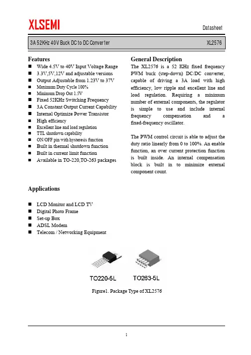
n LCD Monitor and LCD TV
n Portable instrument power supply n Telecom / Networking Equipment
component count.
Figure1. Package Type of XL4015
Pin Configurations
Figure2. Pin Configuration of XL4015 (Top View)
Table 1 Pin Description
Pin Number
Pin Name Description
1
GND
Ground Pin. Care must be taken in layout. This pin should be placed outside of the Schottky Diode to output capacitor ground path to prevent switching current spikes from inducing voltage noise into XL4015.
2 FB Feedback Pin (FB). Through an external resistor divider network, FB senses the output voltage and regulates it. The feedback threshold voltage is 1.25V .
3 SW Power Switch Output Pin (SW). SW is the switch node that supplies power to the output.
4 VC Internal V oltage Regulator Bypass Capacity. In typical system application, The VC pin connect a 1uf capacity to VIN.
5 VIN
Supply V oltage Input Pin. XL4015 operates from a 8V to 36V DC voltage. Bypass Vin to GND with a suitably large capacitor to eliminate noise on the input.
Function Block
Figure3. Function Block Diagram of XL4015
Typical Application Circuit
Figure4. XL4015 Typical Application Circuit (VIN=8V~36V, VOUT=5V/5A)
Order Information Marking ID Package Type Packing Type Supplied As
XL4015E1 XL4015E1 TO263-5L 800 Units on Tape & Reel XLSEMI Pb-free products, as designated with “E1” suffix in the par number, are RoHS compliant.
Absolute Maximum Ratings(Note1)
Parameter Symbol Value Unit Input Voltage Vin -0.3 to 40 V Feedback Pin Voltage V FB-0.3 to Vin V Output Switch Pin Voltage V Output-0.3 to Vin V Power Dissipation P D Internally limited mW Thermal Resistance (TO263-5L)
R JA30 ºC/W (Junction to Ambient, No Heatsink, Free Air)
Operating Junction Temperature T J-40 to 125 ºC Storage Temperature T STG-65 to 150 ºC Lead Temperature (Soldering, 10 sec) T LEAD260 ºC ESD (HBM) >2000 V Note1: Stresses greater than those listed under Maximum Ratings may cause permanent damage to the device. This is a stress rating only and functional operation of the device at these or any other conditions above those indicated in the operation is not implied. Exposure to absolute maximum rating conditions for extended periods may affect reliability.
XL4015 Electrical Characteristics
T a = 25℃;unless otherwise specified.
Symbol Parameter Test Condition Min. Typ. Max. Unit System parameters test circuit figure4
VFB Feedback
V oltage
Vin = 8V to 40V, V out=5V
Iload=0.5A to 5A
1.225 1.25 1.275 V
Efficiency ŋVin=12V ,V out=5V
Iout=5A
- 87 - %
Efficiency ŋVin=24V ,V out=12V
Iout=4A
- 93 - %
Electrical Characteristics (DC Parameters)
Vin = 12V, GND=0V, Vin & GND parallel connect a 220uf/50V capacitor; Iout=500mA, T a = 25℃; the others floating unless otherwise specified.
Parameters Symbol Test Condition Min. Typ. Max. Unit Input operation voltage Vin 8 36 V Quiescent Supply Current I q V FB =Vin 2.1 5 mA Oscillator Frequency Fosc 144 180 216 KHz Output Short Frequency Fosp 48 KHz Switch Current Limit I L V FB =0 7 A Max. Duty Cycle D MAX V FB=0V 100 %
Output Power PMOS Rdson V FB=0V, Vin=12V,
I SW=5A
60 80 mohm
Typical System Application (VOUT=5V/5A)
Efficiency VS Output current
Figure6. XL4015 System Efficiency Curve
Typical System Application (VOUT=12V/4A)
Efficiency VS Output current
Figure8. XL4015 System Efficiency Curve
Logic level signals shutdown function can be used in typical system application with external components. When the TTL high voltage above 3.3V(referenced to ground, lower than VIN), the converter will shutdown, input current less than 5mA; when the TTL Low voltage below
0.8V(referenced to ground), the converter will turn on.
Figure9. XL4015 Typical Application Circuit
Package Information TO263-5L。