A single-photonsensitiveebCMOScamera
- 格式:pdf
- 大小:1.35 MB
- 文档页数:9
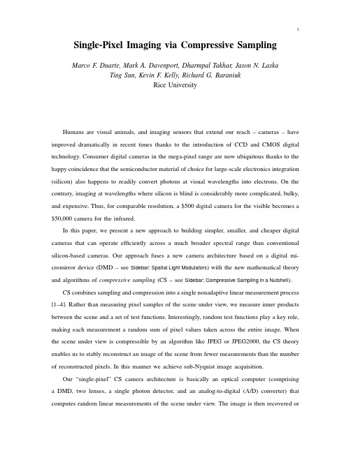
Single-Pixel Imaging via Compressive SamplingMarco F.Duarte,Mark A.Davenport,Dharmpal Takhar,Jason skaTing Sun,Kevin F.Kelly,Richard G.BaraniukRice UniversityHumans are visual animals,and imaging sensors that extend our reach–cameras–have improved dramatically in recent times thanks to the introduction of CCD and CMOS digital technology.Consumer digital cameras in the mega-pixel range are now ubiquitous thanks to the happy coincidence that the semiconductor material of choice for large-scale electronics integration (silicon)also happens to readily convert photons at visual wavelengths into electrons.On the contrary,imaging at wavelengths where silicon is blind is considerably more complicated,bulky, and expensive.Thus,for comparable resolution,a$500digital camera for the visible becomes a $50,000camera for the infrared.In this paper,we present a new approach to building simpler,smaller,and cheaper digital cameras that can operate efficiently across a much broader spectral range than conventional silicon-based cameras.Our approach fuses a new camera architecture based on a digital mi-cromirror device(DMD–see Sidebar:Spatial Light Modulators)with the new mathematical theory and algorithms of compressive sampling(CS–see Sidebar:Compressive Sampling in a Nutshell).CS combines sampling and compression into a single nonadaptive linear measurement process [1–4].Rather than measuring pixel samples of the scene under view,we measure inner products between the scene and a set of test functions.Interestingly,random test functions play a key role, making each measurement a random sum of pixel values taken across the entire image.When the scene under view is compressible by an algorithm like JPEG or JPEG2000,the CS theory enables us to stably reconstruct an image of the scene from fewer measurements than the number of reconstructed pixels.In this manner we achieve sub-Nyquist image acquisition.Our“single-pixel”CS camera architecture is basically an optical computer(comprising a DMD,two lenses,a single photon detector,and an analog-to-digital(A/D)converter)that computes random linear measurements of the scene under view.The image is then recovered orFig.1.Aerial view of the single-pixel compressive sampling(CS)camera in the lab[5].processed from the measurements by a digital computer.The camera design reduces the required size,complexity,and cost of the photon detector array down to a single unit,which enables the use of exotic detectors that would be impossible in a conventional digital camera.The random CS measurements also enable a tradeoff between space and time during image acquisition.Finally, since the camera compresses as it images,it has the capability to efficiently and scalably handle high-dimensional data sets from applications like video and hyperspectral imaging.This article is organized as follows.After describing the hardware,theory,and algorithms of the single-pixel camera in detail,we analyze its theoretical and practical performance and compare it to more conventional cameras based on pixel arrays and raster scanning.We also explain how the camera is information scalable in that its random measurements can be used to directly perform simple image processing tasks,such as target classification,withoutfirst reconstructing the underlying imagery.We conclude with a review of related camera architectures and a discussion of ongoing and future work.I.The Single-Pixel CameraArchitectureThe single-pixel camera is an optical computer that sequentially measures the inner products y[m]= x,φm between an N-pixel sampled version x of the incident light-field from the scene under view and a set of two-dimensional(2D)test functions{φm}[5].As shown in Fig.1,thelight-field is focused by biconvex Lens1not onto a CCD or CMOS sampling array but rather onto a DMD consisting of an array of N tiny mirrors(see Sidebar:Spatial Light Modulators).Each mirror corresponds to a particular pixel in x andφm and can be independently oriented either towards Lens2(corresponding to a1at that pixel inφm)or away from Lens2(corre-sponding to a0at that pixel inφm).The reflected light is then collected by biconvex Lens2and focused onto a single photon detector(the single pixel)that integrates the product x[n]φm[n]to compute the measurement y[m]= x,φm as its output voltage.This voltage is then digitized by an A/D converter.Values ofφm between0and1can be obtained by dithering the mirrors back and forth during the photodiode integration time.To obtainφm with both positive and negative values(±1,for example),we estimate and subtract the mean light intensity from each measurement,which is easily measured by setting all mirrors to the full-on1position.To compute CS randomized measurements y=Φx as in(1),we set the mirror orientations φm randomly using a pseudo-random number generator,measure y[m],and then repeat the process M times to obtain the measurement vector y.Recall from Sidebar:Compressive Sampling in a Nutshell that we can set M=O(K log(N/K))which is≪N when the scene being imaged is compressible by a compression algorithm like JPEG or JPEG2000.Since the DMD array is programmable,we can also employ test functionsφm drawn randomly from a fast transform such as a Walsh,Hadamard,or Noiselet transform[6,7].The single-pixel design reduces the required size,complexity,and cost of the photon detector array down to a single unit,which enables the use of exotic detectors that would be impossible in a conventional digital camera.Example detectors include a photomultiplier tube or an avalanche photodiode for low-light(photon-limited)imaging(more on this below),a sandwich of several photodiodes sensitive to different light wavelengths for multimodal sensing,a spectrometer for hyperspectral imaging,and so on.In addition to sensingflexibility,the practical advantages of the single-pixel design include the facts that the quantum efficiency of a photodiode is higher than that of the pixel sensors in a typical CCD or CMOS array and that thefill factor of a DMD can reach90%whereas that of a CCD/CMOS array is only about50%.An important advantage to highlight is the fact that each CS measurement receives about N/2times more photons than an average pixel sensor,which significantly reduces image distortion from dark noise and read-out noise.Theoretical advantages(a)(b)(c)Fig.2.Single-pixel photo album.(a)256×256conventional image of a black-and-white R.(b)Single-pixel camera reconstructed image from M=1300random measurements(50×sub-Nyquist).(c)256×256 pixel color reconstruction of a printout of the Mandrill test image imaged in a low-light setting using a single photomultiplier tube sensor,RGB colorfilters,and M=6500random measurements.that the design inherits from the CS theory include its universality,robustness,and progressivity.The single-pixel design falls into the class of multiplex cameras[8].The baseline standard for multiplexing is classical raster scanning,where the test functions{φm}are a sequence of delta functionsδ[n−m]that turn on each mirror in turn.As we will see below,there are substantial advantages to operating in a CS rather than raster scan mode,including fewer total measurements (M for CS rather than N for raster scan)and significantly reduced dark noise.Image acquisition examplesFigure2(a)and(b)illustrates a target object(a black-and-white printout of an“R”)x and reconstructed image x taken by the single-pixel camera prototype in Fig.1using N=256×256 and M=N/50[5].Fig.2(c)illustrates an N=256×256color single-pixel photograph of a printout of the Mandrill test image taken under low-light conditions using RGB colorfilters and a photomultiplier tube with M=N/10.In both cases,the images were reconstructed using Total Variation minimization,which is closely related to wavelet coefficientℓ1minimization[2].Structured illumination configurationIn a reciprocal configuration to that in Fig.1,we can illuminate the scene using a projector displaying a sequence of random patterns{φm}and collect the reflected light using a single lens and photodetector.Such a“structured illumination”setup has advantages in applications where we can control the light source.In particular,there are intriguing possible combinations of single-pixel imaging with techniques such as3D imaging and dual photography[9].Shutterless video imagingWe can also acquire video sequences using the single-pixel camera.Recall that a traditional video camera opens a shutter periodically to capture a sequence of images(called video frames) that are then compressed by an algorithm like MPEG that jointly exploits their spatio-temporal redundancy.In contrast,the single-pixel video camera needs no shutter;we merely continuously sequence through randomized test functionsφm and then reconstruct a video sequence using an optimization that exploits the video’s spatio-temporal redundancy[10].If we view a video sequence as a3D space/time cube,then the test functionsφm lie concentrated along a periodic sequence of2D image slices through the cube.A na¨ıve way to reconstruct the video sequence would group the corresponding measurements y[m]into groups where the video is quasi-stationary and then perform a2D frame-by-frame reconstruction on each group.This exploits the compressibility of the3D video cube in the space but not time direction.A more powerful alternative exploits the fact that even though eachφm is testing a different 2D image slice,the image slices are often related temporally through smooth object motions in the video.Exploiting this3D compressibility in both the space and time directions and inspired by modern3D video coding techniques[11],we can,for example,attempt to reconstruct the sparsest video space/time cube in the3D wavelet domain.These two approaches are compared in the simulation study illustrated in Fig.3.We employed simplistic3D tensor product Daubechies-4wavelets in all cases.As we see from thefigure,3D reconstruction from2D random measurements performs almost as well as3D reconstruction from 3D random measurements,which are not directly implementable with the single-pixel camera.II.Single-Pixel Camera TradeoffsThe single-pixel camera is aflexible architecture to implement a range of different multiplex-ing methodologies,just one of them being CS.In this section,we analyze the performance of CS and two other candidate multiplexing methodologies and compare them to the performance of a brute-force array of N pixel sensors.Integral to our analysis is the consideration of Poisson photon counting noise at the detector,which is image-dependent.We conduct two separate analyses to assess the“bang for the buck”of CS.Thefirst is a theoretical analysis that provides general guidance.The second is an experimental study that indicates how the systems typically perform(a)frame32(b)2D meas(c)2D meas(d)3D meas+2D recon+3D recon+3D reconFig.3.Frame32from a reconstructed video sequence using(top row)M=20,000and(bottom row) M=50,000measurements(simulation from[10]).(a)Original frame of an N=64×64×64video of a disk simultaneously dilating and translating.(b)Frame-by-frame2D measurements+frame-by-frame 2D reconstruction;MSE=3.63and0.82,respectively.(c)Frame-by-frame2D measurements+joint3D reconstruction;MSE=0.99and0.24,respectively.(d)Joint3D measurements+joint3D reconstruction; MSE=0.76and0.18,respectively.in practice.Scanning methodologiesThe four imaging methodologies we consider are:•Pixel array(PA):a separate sensor for each of the N pixels receives light throughout the total capture time T.This is actually not a multiplexing system,but we use it as the gold standard for comparison.•Raster scan(RS):a single sensor takes N light measurements sequentially from each of the N pixels over the capture time.This corresponds to test functions{φm}that are delta functions and thusΦ=I.The measurements y thus directly provide the acquired image x.•Basis scan(BS):a single sensor takes N light measurements sequentially from different combinations of the N pixels as determined by test functions{φm}that are not delta functions but from some more general basis[12].In our analysis,we assume a Walsh basis modified to take the values0/1rather than±1;thusΦ=W,where W is the0/1Walsh matrix.The acquired image is obtained from the measurements y by x=Φ−1y=W−1y.•Compressive sampling(CS):a single sensor takes M≤N light measurements sequentially from different combinations of the N pixels as determined by random0/1test functions {φm}.Typically,we set M=O(K log(N/K))which is≪N when the image is com-pressible.In our analysis,we assume that the M rows of the matrixΦconsist of randomlydrawn rows from a0/1Walsh matrix that are then randomly permuted(we ignore thefirst row consisting of all1’s).The acquired image is obtained from the measurements y via a sparse reconstruction algorithm such as BPIC(see Sidebar:Compressive Sampling in a Nutshell).Theoretical analysisIn this section,we conduct a theoretical performance analysis of the above four scanning methodologies in terms of the required dynamic range of the photodetector,the required bit depth of the A/D converter,and the amount of Poisson photon counting noise.Our results are pessimistic in general;we show in the next section that the average performance in practice can be considerably better.Our results are summarized in Table I.An alternative analysis of CS imaging for piecewise smooth images in Gaussian noise has been reported in[13].Dynamic range:Wefirst consider the photodetector dynamic range required to match the performance of the baseline PA.If each detector in the PA has a linear dynamic range of0to D, then it is easy to see that single-pixel RS detector need only have that same dynamic range.In contrast,each Walsh basis test function contains N/21’s,and so directs N/2times more light to the detector.Thus,BS and CS each require a larger linear dynamic range of0to ND/2.On the positive side,since BS and CS collect considerably more light per measurement than the PA and RS,they benefit from reduced detector nonidealities like dark currents.Quantization error:We now consider the number of A/D bits required within the required dynamic range to match the performance of the baseline PA in terms of worst-case quantization distortion.Define the mean-squared error(MSE)between the true image x and its acquired version x as MSE=1ND2−B−1[14].Due to its larger dynamic range,BS requires B+ log2N bits per measurement to reach the same MSE distortion level.Since the distortion of CS reconstruction is up to C N times larger than the distortion in the measurement vector(see Sidebar: Compressive Sensing in a Nutshell),we require up to an additional log2C N bits per measurement. One empirical study has found roughly that C N lies between8and10for a range of different random measurement configurations[15].Thus,BS and CS require a higher-resolution A/D converter than PA and RS to acquire an image with the same worst-case quantization distortion.TABLE IComparison of the four camera scanning methodologies.Raster Scan Compressive Sampling N ND ND NDNB N(B+log2N)P N P(3N−2)P<3C2NM P3C2N, the MSE of CS is lower than that of RS.We emphasize that in the CS case,we have only a fairly loose upper bound and that there exist alternative CS reconstruction algorithms with better performance guarantees,such as the Dantzig Selector[3].Summary:From Table I,we see that the advantages of a single-pixel camera over a PA come at the cost of more stringent demands on the sensor dynamic range and A/D quantization and larger MSE due to photon counting effects.Additionally,the linear dependence of the MSE on the number of image pixels N for BS and RS is a potential deal-breaker for high-resolution imaging.The promising aspect of CS is the logarithmic dependence of its MSE on N through the relationship M=O(K log(N/K)).Experimental resultsSince CS acquisition/reconstruction methods often perform much better in practice than the above theoretical bounds suggest,in this section we conduct a simple experiment using real data from the CS imaging testbed depicted in Fig.1.Thanks to the programmability of the testbed, we acquired RS,BS,and CS measurements from the same hardware.Wefixed the number of A/D converter bits across all methodologies.Figure4shows the pixel-wise MSE for the capture of a N=128×128pixel“R”test image as a function of the total capture time T.Here the MSE combines both quantization and photon counting effects.For CS we took M=N/10total measurements per capture and used a Daubechies-4wavelet basis for the sparse reconstruction.We make two observations.First,the performance gain of BS over RS contradicts the aboveFig.4.Average MSE for Raster Scan(RS),Basis Scan(BS),and Compressive Sampling(CS)single-pixel images as a function of the total image capture time T(real data).worst-case theoretical calculations.We speculate that the contribution of the sensor’s dark current, which is not accounted for in our analysis,severely degrades RS’s performance.Second,the performance gain of CS over both RS and BS is clear:images can either be acquired in much less time for the same MSE or with much lower MSE in the same amount of time.rmation Scalability and the Smashed FilterWhile the CS literature has focused almost exclusively on problems in signal and image reconstruction or approximation,reconstruction is frequently not the ultimate goal.For instance, in many image processing and computer vision applications,data is acquired only for the purpose of making a detection,classification,or recognition decision.Fortunately,the CS framework is information scalable to a much wider range of statistical inference tasks[17–19].Tasks such as detection do not require reconstruction,but only require estimates of the relevant sufficient statistics for the problem at hand.Moreover,in many cases it is possible to directly extract these statistics from a small number of random measurements without ever reconstructing the image.The matchedfilter is a key tool in detection and classification problems that involve searching for a target template in a scene.A complicating factor is that often the target is transformed in some parametric way—for example the time or Doppler shift of a radar return signal;the translation and rotation of a face in a face recognition task;or the roll,pitch,yaw,and scale of a vehicle viewed from an aircraft.The matchedfilter detector operates by forming comparisons between the given test data and all possible transformations of the template tofind the match that optimizes some performance metric.The matchedfilter classifier operates in the same waybut chooses the best match from a number of different potential transformed templates.The na¨ıve approach to matchedfiltering with CS wouldfirst reconstruct the images under consideration and then apply a standard matchedfiltering technique.In contrast,the smashed filter(for dimensionally reduced matchedfilter)performs all of its operations directly on the random measurements[18].The two key elements of the smashedfilter are the generalized likelihood ratio test and the concept of an image appearance manifold[20].If the parametric transformation affecting the template image is well-behaved,then the set of transformed templates forms a low-dimensional manifold in the high-dimensional pixel space R N with the dimension K equal to the number of independent parameters.1Thus,the matchedfilter classifier can be interpreted as classifying a test image according to the closest template manifold in R N.The smashedfilter exploits a recent result that the structure of a smooth K-dimensional manifold in R N is preserved with high probability under a random projection to the lower dimensional space R M as long as M=O(K log N)[21].This is reminiscent of the number of measurements required for successful CS but with K now the manifold dimension.Thus,to classify an N-pixel test image,we can alternatively compare M random measurements of the test image to the M-dimensional projections(using the sameΦ)of the candidate image template manifolds.The upshot is that all necessary computations can be made directly in R M rather than in R N.As in the conventional matchedfilter,a byproduct of the closest manifold search is an estimate of the template parameters that best match the test image.Previous work in the computer science community(the other“CS”)has also employed the Johnson-Lindenstrauss lemma[22] to reduce the data dimensionality prior to computing features for classification;however,they have not considered the intrinsic manifold structure manifested in many image processing and computer vision settings.Figure5demonstrates the effectiveness of smashedfiltering for the task of classifying an N= 128×128pixel test image under an unknown translation in the vertical and horizontal directions (hence K=2).The three classes correspond to different translations of a bus,truck,or tank.The test data was generated randomly from one of the three classes.The random measurements were 1For the purposes of the discussion here,a K-dimensional manifold can be interpreted as a K-dimensional hypersurface in R N.Fig.5.Smashedfilter image classification performance plotted as a function of the number of random measurements M from a simulated single-pixel CS camera and the total acquisition time T.produced using a simulated single-pixel CS camera that takes into account the Poisson photon counting noise associated with a total measurement interval of length T.We average over10,000 iterations of each experiment.We see that increasing the number of measurements improves performance atfirst;however,performance then degrades due to the reduced time available to obtain each measurement.Correspondingly,increasing the total capture time improves the performance of the algorithm.IV.Other Multiplexing Camera ArchitecturesTwo notable existing DMD-driven imaging applications involve confocal microscopy(which relates closely to the raster scan strategy studied above)[23,24]and micro-optoelectromechanical (MOEM)systems[12,25,26].In a MOEM system,a DMD is positioned between the scene and the sensing array to perform column-wise multiplexing by allowing only the light from the desired pixels to pass through.In[12,25]the authors propose sets of N Hadamard patterns,which enables simple demultiplexing,and randomized Hadamard patterns,which yield a uniform signal-to-noise ratio among the measurements.Other compressive cameras developed to date include[27,28],which employ optical elements to perform transform coding of multispectral images.These designs obtain sampled outputs that correspond to coded information of interest,such as the wavelength of a given light signal or the transform coefficients in a basis of interest.The elegant hardware designed for these purposes uses optical projections,group testing,and signal inference.Recent work in[29]has compared several single and multiple pixel imaging strategies of varying complexities;their simulationresults for Poisson counting noise agree closely with those above.Finally,in[30]the authors use CS principles and a randomizing lens to boost both the resolution and robustness of a conventional digital camera.V.ConclusionsFor certain applications,CS promises to substantially increase the performance and capabil-ities of data acquisition,processing,and fusion systems while lowering the cost and complexity of deployment.A useful practical feature of the CS approach is that it off-loads processing from data acquisition(which can be complicated and expensive)into data reconstruction or processing (which can be performed on a digital computer,perhaps not even co-located with the sensor).We have presented an overview of the theory and practice of a simple yetflexible single-pixel architecture for CS based on a DMD spatial light modulator.While there are promising potential applications where current digital cameras have difficulty imaging,there are clear tradeoffs and challenges in the single-pixel design.Our current and planned work involves better understanding and addressing these tradeoffs and challenges.Other potential avenues for research include extending the single-pixel concept to wavelengths where the DMD fails as a modulator,such as THz and X-rays.Sidebar:Compressive Sampling in a NutshellCompressive Sampling(CS)is based on the recent understanding that a small collection of nonadaptive linear measurements of a compressible signal or image contain enough information for reconstruction and processing[1–3].For a tutorial treatment see[4]or the paper by Romberg in this issue.The traditional approach to digital data acquisition samples an analog signal uniformly at or above the Nyquist rate.In a digital camera,the samples are obtained by a2D array of N pixel sensors on a CCD or CMOS imaging chip.We represent these samples using the vector x with elements x[n],n=1,2,...,N.Since N is often very large,e.g.in the millions for today’s consumer digital cameras,the raw image data x is often compressed in the following multi-step transform coding process.Thefirst step in transform coding represents the image in terms of the coefficients{αi}of an orthonormal basis expansion x= N i=1αiψi where{ψi}N i=1are the N×1basis vectors.Forming the coefficient vectorαand the N×N basis matrixΨ:=[ψ1|ψ2|...|ψN]by stacking the vectors{ψi}as columns,we can concisely write the samples as x=Ψα.The aim is to find a basis where the coefficient vectorαis sparse(where only K≪N coefficients arenonzero)or r-compressible(where the coefficient magnitudes decay under a power law withscaling exponent−r).For example,natural images tend to be compressible in the discrete cosinetransform(DCT)and wavelet bases on which the JPEG and JPEG-2000compression standardsare based.The second step in transform coding encodes only the values and locations of the Ksignificant coefficients and discards the rest.This sample-then-compress framework suffers from three inherent inefficiencies:First,wemust start with a potentially large number of samples N even if the ultimate desired K is small.Second,the encoder must compute all of the N transform coefficients{αi},even though it will discard all but K of them.Third,the encoder faces the overhead of encoding the locations of the large coefficients.As an alternative,CS bypasses the sampling process and directly acquires a condensedrepresentation using M<N linear measurements between x and a collection of test functions{φm}M m=1as in y[m]= x,φm .Stacking the measurements y[m]into the M×1vector y and the test functionsφT m as rows into an M×N matrixΦwe can writey=Φx=ΦΨα.(1)The measurement process is non-adaptive in thatΦdoes not depend in any way on the signal x.The transformation from x to y is a dimensionality reduction and so loses information in general.In particular,since M<N,given y there are infinitely many x′such thatΦx′=y. The magic of CS is thatΦcan be designed such that sparse/compressible x can be recovered exactly/approximately from the measurements y.While the design ofΦis beyond the scope of this review,an intriguing choice that works with high probability is a random matrix.For example,we can draw the elements ofΦas independent and identically distributed(i.i.d.)±1random variables from a uniform Bernoulli distribution[22]. Then,the measurements y are merely M different randomly signed linear combinations of the elements of x.Other possible choices include i.i.d.,zero-mean,1/N-variance Gaussian entries (white noise)[1–3,22],randomly permuted vectors from standard orthonormal bases,or random。

㊃专题㊃通信作者:刘俊艳,E m a i l :j u n ya n l i u 2003@163.c o m 磁敏感加权成像突出血管征在卒中患者中的应用价值贾亚南,刘俊艳(河北医科大学第三医院神经内科,河北石家庄050000) 摘 要:急性卒中患者低灌注区域内脑组织局部血管内氧摄取率增高,导致毛细血管及静脉内脱氧血红蛋白与含氧血红蛋白比值增高㊂利用磁敏感加权成像对脱氧血红蛋白等顺磁性物质的敏感性,脱氧血红蛋白浓度高的血管在S W I 上呈现为突出血管征(p r o m i n e n t v e s s e l s i g n ,P V S )㊂P V S 的出现可用于评估缺血半暗带及脑灌注疗效,也预示了侧支循环建立及脑储备能力,P V S 的存在也与卒中预后有一定关系㊂关键词:卒中;磁敏感加权成像;突出血管征中图分类号:R 743 文献标志码:A 文章编号:1004-583X (2017)09-0737-05d o i :10.3969/j.i s s n .1004-583X.2017.09.001A p p l i c a t i o nv a l u e o f p r o m i n e n t v e s s e l s i g no nm a g n e t i c s u s c e p t i b i l i t y w e i g h t e d i m a g i n gi n s t r o k e J i aY a n a n ,L i u J u n ya n D e p a r t m e n t o f N e u r o l o g y ,t h eT h i r d H o s p i t a l o f H eb e iM e d ic a lU n i v e r s i t y ,S h i j i a z h u a n g 050000,C h i n a C o r r e s p o nd i n g a u t h o r :L i uJ u n y a n ,E m a i l :j u n ya n l i u 2003@163.c o m A B S T R A C T :I n t h e p a t i e n t s w i t h a c u t e s t r o k e ,t h e o x y ge n e x t r a c t i o nf r a c t i o n (O E F )i si n c r e a s e di n t h e h y p o p e r f u s e d p a r e n c h y m a ,r e s u l t i ng i na n i n c r e a s e i n th e r a ti oo f d e o x y g e n a t e dh e m o g l o b i n t oo x y g e n a t e dh e m o gl o b i n i n t h ec a p i l l a r y a n d v e i n .B e c a u s eS u s c e p t i b i l i t y w e i g h t e di m a g i n g (S W I )i se x q u i s i t e l y s e n s i t i v et o p a r a m a gn e t i c s u b s t a n c e s ,s u c ha sd e o x y h e m o g l o b i n ,p r o m i n e n tv e s s e ls i g n (P V S )w i l la p pe a ro nS W Iw h e nt h ec o n c e n t r a t i o nof d e o x y h e m o gl o b i n i n t h e v e i n s i n c r e a s e s .T h e p r e s e n c eo fP V Sc a nb eu s e dt oa s s e s s i s c h e m i c p e n u m b r aa n dc e r e b r a l r e p e r f u s i o n t h e r a p y ,a n da l s o p r e d i c t t h e e s t a b l i s h m e n t o f c o l l a t e r a l c i r c u l a t i o na n db r a i nr e s e r v e c a p a c i t y.M o r e o v e r ,t h e p r e s e n c e o fP V S i s a l s o r e l a t e d t o t h e p r o gn o s i s o f s t r o k e .K E Y W O R D S :s t r o k e ;s u s c e p t i b i l i t y w e i g h t e d i m a g i n g ;p r o m i n e n t v e s s e l s i gn 刘俊艳,硕士生导师㊁二级教授㊂河北医科大学第三医院神经内科主任,河北省青年突出贡献专家,白求恩专家委员会常委,国家卫计委脑卒中防治委员会委员㊂中国卒中学会委员,中国卒中学会脑血流和代谢分会副主委,中国医师学会委员,中国医师学会脑血管学组委员,河北省卒中学会副主委,河北省质量控制专家委员会副主委,河北省医学会神经病学分会副主任委员㊂磁敏感加权成像(s u s c e p t i b i l i t y w e i gh t e d i m a g i n g ,S W I )是在梯度回波序列(g r a d i e n t r e c a l l e d e c h o ,G R E )基础上进一步发展而来的一种新的成像技术㊂其利用不同脑组织磁敏感性的差异,使含铁血黄素㊁脱氧血红蛋白㊁铁沉积㊁钙化等顺磁性物质得以显像[1]㊂由此,S W I 广泛应用于脑挫伤㊁脑卒中㊁脑退行性病变㊁脑血管畸形㊁颅内钙化㊁脑肿瘤等疾病的鉴别诊断[2-6],尤其对于急性卒中患者,S W I可显示下述3个重要的病理学异常:①探查微出血灶和出血转化[7];②显示低灌注区域内的突出血管征(p r o m i n e n t v e s s e l s i gn ,P V S )[8];③检测具有血栓识别能力的磁敏感血管征(s u s c e p t i b i l i t y ve s s e l s i gn ,S V S )[9]㊂本文重点论述S W I 显示的P V S 在急性卒中临床应用㊂1 P V S 的成像的原理和机制灌注减低区域内明显的低信号血管信号影被称之为P V S ㊂P V S 的产生源自于急㊁慢性脑灌注不良患者经由血液动力学障碍的失代偿期,脑血管的自我调节能力不足以代偿灌注量持续降低时,脑组织代偿地增加了其自血管内氧的摄取率(o x y ge n e x t r a c t i o nf r a c t i o n ,O E F ),通过高O E F 弥补贫困灌注的不足,从而导致毛细血管及静脉血内脱氧血红蛋白与含氧血红蛋白比值增高,这种比例的变化在磁共振成像(m ag n e t i cr e s o n a n c ei m a g i n g,MR I ),S W I 上显示为低信号[10],即P V S 的出现㊂故P V S 的存在说明脑血液动力学障碍进入失代偿Ⅱ期即 贫困灌注期㊂P V S 最常见于患侧脑组织皮层浅表静脉分布区,也可见于急性缺血性卒中患侧大脑深静脉部位[11-12]㊂此外,本作者发现基底节区脑出血患者于病后6个月复查时,其S W I 也可于患侧发现P V S㊃737㊃‘临床荟萃“ 2017年9月5日第32卷第9期 C l i n i c a l F o c u s ,S e pt e m b e r 5,2017,V o l 32,N o .9Copyright ©博看网. All Rights Reserved.(图1),推测P V S的出现与患侧皮层静脉血回流受阻或脑组织代谢活跃有关㊂也有学者发现肺栓塞患者其颅脑S W I也存在广泛P V S,这是因为肺栓塞患者血氧饱和度降低,此时尽管O E F不增加,静脉中脱氧血红蛋白浓度也较正常高[13]㊂图155岁中年男性,左侧基底节区出血半年后复查,S W I示:病灶侧可见P V S2P V S与缺血半暗带评估急性缺血性卒中的病灶是由核心坏死区㊁周围的缺血半暗带㊁良性低灌注区及正常供血区共同组成㊂缺血中心坏死区与缺血半暗带是一个动态演变的病理生理过程㊂随着缺血时间的延长和低灌注程度的加重,中心坏死区范围会逐渐扩大,而缺血半暗带会逐渐缩小[14]㊂因此,及时识别和挽救缺血半暗带对于急性脑梗死患者的临床预后至关重要㊂既往多利用磁共振灌注成像(p e r f u s i o n w e i g h t e d i m a g i n g,P W I)的平均通过时间((m e a n t r a n s i t t i m e,MT T)㊁达峰时间(t i m e t o p e a k,T T P)的延长及脑血流量(c e r e b r a l b l o o d f l o w,C B F)与脑血容量(c e r e b r a l b l o o dv o l u m e,C B V)的不匹配来评估半暗带,明确脑组织低灌注区域㊂如临床中将P W I-D W I的不匹配区表示缺血半暗带[15-16],用于评估超时溶栓或不确定发病时间患者的溶栓获益与风险㊂新近研究发现,S W I所示P V S的空间分布与P W I中MT T延长的区域相似,A S P E C T S-S W I与A S P E C T S-P W I评分具有很强的相关性[17-18]㊂进一步研究表明:O E F增高与MT T的延长显著相关[19-20],而P V S也间接提示O E F增加㊂因此,有学者提出,S W I-DW I也可用来评估缺血半暗带[21-24],其与DW I-P W I相互补充,但不能替代[25]㊂原因是: S W I上显示的P V S仅间接地反映脑组织的代谢储备及氧代谢,但不能量化,对半暗带的评估还缺少可靠的标准化依据;除此之外,有研究发现并非P W I显示的所有低灌注区均可通过S W I检测到P V S;而S W I的优势是无需注入对比剂及图像后处理来获取图像信息,可以节省检查时间和费用,降低患者对对比剂过敏的风险,尤其适用于严重肾功不全的患者;此外,利用不同物质顺磁性强弱的差异,S W I还可以监测到血管内血栓及微出血改变,用于血管急性闭塞性疾病的诊断及出血风险评估[25-26]㊂值得注意的是,有研究发现:卒中发作8小时后的患者,S W I仍可见到P V S的出现,此时,S W I-DW I 的不匹配区不再代表缺血半暗带,往往代表 贫困灌注 [27]㊂3P V S与侧支循环的关系侧支循环的开放是脑血流动力学障碍患者首要的代偿途径,卒中急性期侧支循环的建立利于缺血脑组织的再灌注㊂研究显示[28-30],良好的侧支循环可有效增加半暗带面积㊁减少缺血中心坏死区范围,从而延长卒中救治时间窗㊁增加静脉溶栓和机械取栓的成功率,降低溶栓后出血转化㊁改善脑组织缺血缺氧状况,改善卒中预后㊁减少卒中复发风险㊂故全面㊁准确地评估脑侧支循环并及时进行干预治疗,对个体化治疗方案的制定至关重要㊂侧支循环的常规检测方法包括血管影像学检测及灌注影像学两种㊂血管影像学检测方法包括经颅多普勒(t r a n s c r a n i a l d o p p l e r,T C D)㊁经颅彩色多普勒超声(t r a n s c r a n i a lc o l o r-c o d e dd u p l e xs o n o g r a p h y,T C C S/ T C C D)㊁磁共振血管造影(m a g n e t i c r e s o n a n c e a n g i o g r a p h y,M R A)㊁计算机断层血管造影(c o m p u t e d t o m o g r a p h y a n g i o g r a p h y,C T A)㊁数字减影血管造影(d i g i t a ls u b t r a c t i o n a n g i o g r a p h y, D S A)等,C T A㊁尤其是D S A作为血管影像学检测的金标准,虽具有敏感性及特异性高的优点,可以检测1~3级侧支循环,但均需静脉注射造影剂,且检查价格昂贵,临床使用具有一定的局限性;而M R A及T C D作为初筛检查技术,仅仅能检测一㊁二级侧支循环,评估敏感性相对较低,也有各自的缺陷㊂而灌注影像学包括C T灌注(C T p e r f u s i o n,C T P)㊁P W I㊁单光子发射计算机断层成像术(s i n g l e-p h o t o ne m i s s i o n c o m p u t e d t o m o g r a p h y,S P E C T)㊁正电子发射断层成像术(p o s i t r o ne m i s s i o n t o m o g r a p h y,P E T)及动脉自旋标记灌注技术(a r t e r i a l s p i nl a b e l i n g,A S L)等,主要通过MT T㊁T T P㊁C B F㊁C B V等参数评估缺血局部脑灌注情况,反映的是微动脉及毛细血管水平的侧支循环状态,缺陷是不能明确其上游动脉的来源㊂新近研究表明S W I显示的P V S与侧支循环有一定相关性[26,31-32]㊂V e r m a等[26]以33例M1段急性闭塞的卒中患者作为研究对象,依据D S A所示软㊃837㊃‘临床荟萃“2017年9月5日第32卷第9期 C l i n i c a l F o c u s,S e p t e m b e r5,2017,V o l32,N o.9Copyright©博看网. All Rights Reserved.脑膜动脉的代偿情况将患者分为:侧支循环良好者20例,侧支循环较差者13例;比较了两组患者各自在DW I ㊁P V S ㊁MT T 的A S P E C T S 评分㊂结果发现,侧支循环良好组患者P V S -A S P E C T S 评分显著高于侧支循环较差组(4.1v s 2.69;P =0.039)㊂由此认为:S W I 显示的P V S 显影程度与软脑膜动脉侧支开放程度有关,侧支循环好的P V S 显影较少,反之亦然㊂而该研究中两组患者MT T -A S P E C T S 评分都显著低于P V S -A S P E C T S (1.0v s3.5;P <0.001)评分,提示MT T 显示的灌注不良面积大于P V S 的面积㊂该现象在侧支循环良好个体中尤为显著,考虑其发生机制可能是良好侧支循环的建立,增加了缺血半暗带的血氧供给量,减少了脑组织对局部血管的O E F ,从而使S W I 显示的P V S 面积小于MT T显示的灌注不良区域㊂然而,P a r k 等[31-32]研究则认为,S W I 显示的P V S 与侧支循环良好有关㊂因为,良好的侧支循环可延长缺血半暗带的维持时间,减少缺血半暗带向坏死区的转化,而P V S 的存在意义等同于P W I,可用来评估缺血半暗带的大小㊂因此,侧支循环良好者其S W I 显示的P V S 面积可能也更为广泛㊂所以,有关S W I 所示P V S 意义及与侧支循环的关系尚还存有争议,需要大样本研究P V S 与侧支循环的相关性㊂4 P V S 对灌注治疗疗效的评估P V S 作为反应脑组织代谢状态的指标,对于评估治疗前后受累脑组织低灌注程度㊁灌注不良范围及血管再通后再灌注状态具有重要意义㊂脑组织得到有效再灌注治疗后,静脉中脱氧血红蛋白的浓度恢复正常,S W I 显示的P V S 消失[33-34]㊂B a i k 等[34]研究了19例颅内大动脉急性闭塞患者的S W I 成像,以健侧静脉显影作对照,观察了再灌注治疗后患侧P V S 改变与预后关系㊂结果显示:再灌注治疗后患侧P V S 显影等同于对侧静脉者(图2)有良好的再灌注及临床预后;而灌注治疗后患侧P V S 较健侧静脉少者,提示脑组织已发生不可逆损害,坏死的组织细胞代谢率减低,O E F 也随之下降,从而使静脉显影较对侧减少㊂此时的再灌注治疗属于无效灌注,且可能造成再灌注损伤,临床预后差㊂因此,利用S W I 显示再灌注治疗前后P V S 的变化来反应脑组织的代谢状态,从而评估灌注治疗疗效,指导临床及预后评估㊂值得注意的是,利用P V S 评估再灌注治疗效果时,应在接受治疗后尽可能短的时间内进行S W I 检查,因为绝大多数患者即使不接受溶栓治疗,其P V S在发病48小时内也将自然消褪[35]㊂图2 B a i k 等[34]观察再灌注治疗后S W I 显示的P V S 改变的研究中的1例患者 a .左侧颈内动脉及左侧大脑中动脉闭塞,溶栓前DW I 示左侧基底节区梗死灶;b .溶栓前的S W I 左侧大脑中动脉供血区可见广泛的P V S ;c .左侧颈内动脉及大脑中动脉恢复再灌注,溶栓1.5小时后其D W I 显示的梗死灶未进一步扩大;d .溶栓1.5小时后其S W I 显示的P V S 消失㊃937㊃‘临床荟萃“ 2017年9月5日第32卷第9期 C l i n i c a l F o c u s ,S e pt e m b e r 5,2017,V o l 32,N o .9Copyright ©博看网. All Rights Reserved.5P V S对卒中预后的预测价值基于上述,P V S对急性缺血性卒中的临床预测价值尚存争议㊂一些人认为,广泛存在的P V S可能代表缺血半暗带,表示患者可挽救脑组织面积较大,静脉溶栓㊁机械取栓等创伤性治疗可获益,临床预后较好㊂L o u等[36]进行的一项回顾性队列研究表明:存在P V S-DW I不匹配的患者溶栓预后较无P V S-DW I不匹配区患者好㊂P a y a b v a s h等[37]以150例急性大脑中动脉闭塞患者作为研究对象,所有患者均接受标准内科治疗,且接受S W I与DW I检测,评估两者的不匹配区面积与临床预后的关系㊂结果显示:P V S-DW I不匹配区的存在的患者其DW I显示的病灶越小㊁3个月时临床预后较好㊂也有学者认为,P V S的出现提示脑组织处于 贫困灌注 状态,代表脑组织的储备功能衰竭,是早期神经功能恶化㊁梗死灶扩大㊁卒中进展及不良预后的影像标志[8-9,18,27]㊂国外研究显示:P V S可反映脑组织低灌注的程度,无P V S的患者溶栓治疗后神经功能改善情况优于P V S出现的患者[33]㊂此外,新近的研究通过S W I观察急性卒中患者的深部静脉显像,发现患侧深部静脉-丘纹静脉的突出与急性卒中患者溶栓后不良预后有很强的相关性[11]㊂他们认为,丘纹静脉的突出是因为其脱氧血红蛋白浓度较高,反映其所引流区的脑组织处于低灌注状态,并可能与较差的侧支循环有关,使缺血半暗带持时较短,若得不到及时再灌注治疗,溶栓后可能预后不良㊂然而,也有小样本研究认为P V S与临床预后无关[38]㊂上述研究存在着样本量小㊁接受S W I检查的时间不一致,患者接受的治疗措施迥异等问题,可能影响研究结论,需要大样本的R C T试验进一步研究㊂综上所述,S W I显示的P V S可反应组织的代谢状态,用于评估缺血半暗带及脑灌注疗效,间接评估侧支循环开放程度,利于卒中预后评价㊂然而,目前有关急性卒中患者S W I显示的P V S的研究有限,有待进一步研究证实㊂参考文献:[1] H a a c k eE M,X uY,C h e n g Y C,e t a l.S u s c e p t i b i l i t y w e i g h t e di m a g i n g(S W I)[J].M a g nR e s o n M e d,2004,52(3):612-618.[2] T a n I L,v a n S c h i j n d e l R A,P o u w e l s P J,e t a l.M Rv e n o g r a p h y o f m u l t i p l e s c l e r o s i s[J].A J N R A m JN e u r o r a d i o l,2000,21(6):1039-1042.[3] T h a m b u r a j K,R a d h a k r i s h n a n V V,T h o m a s B,e t a l.I n t r a t u m o r a l m i c r o h e m o r r h a g e so n T2*-w e i g h t e d g r a d i e n t-e c h o i m a g i n g h e l p sd if f e r e n t i a t ev e s t i b u l a rs c h w a n n o m af r o mm e n i n g i o m a[J].A J N R A mJN e u r o r a d i o l,2008,29(3):552-557.[4] T h o m a sB,S o m a s u n d a r a m S,T h a m b u r a j K,e ta l.C l i n i c a la p p l i c a t i o n s o fs u s c e p t ib i l i t y w e i g h t e d M R i m a g i n g o ft h eb r a i n-a p ic t o r i a l r e v i e w[J].N e u r o r ad i o l o g y,2008,50(2):105-116.[5] T o n g K A,A s h w a lS,H o l s h o u s e rB A,e ta l.H e m o r r h a g i cs h e a r i n g l e s i o n s i n c h i l d r e n a n d a d o l e s c e n t sw i t h p o s t t r a u m a t i cd i f f u s ea x o n a l i n j u r y:i m p r o ve dd e t e c t i o na n di n i t i a lr e s u l t s[J].R a d i o l o g y,2003,227(2):332-339.[6] H i n g w a l aD,K e s a v a d a sC,T h o m a sB,e t a l.C l i n i c a l u t i l i t yo f s u s c e p t i b i l i t y-w e i g h t e di m a g i n g i nv a s c u l a rd i s e a s e so f t h eb r a i n[J].N e u r o l I n d i a,2010,58(4):602-607.[7]S a n t h o s hK,K e s a v a d a sC,T h o m a sB,e ta l.S u s c e p t i b i l i t yw e i g h t e d i m a g i n g:an e wt o o l i n m a g n e t i c r e s o n a n c e i m a g i n go f s t r o k e[J].C l i nR a d i o l,2009,64(1):74-83.[8] C h e nC Y,C h e nC I,T s a i F Y,e t a l.P r o m i n e n t v e s s e l s i g no ns u s c e p t i b i l i t y-w e i g h t e d i m a g i n g i na c u t es t r o k e:p r e d i c t i o no fi n f a r c t g r o w t ha n d c l i n i c a l o u t c o m e[J].P L o S O n e,2015,10(6):e0131118.[9] P a r k MG,Y o o n C H,B a i kS K,e ta l.S u s c e p t i b i l i t y v e s s e ls i g nf o ri n t r a-a r t e r i a lt h r o m b u si n a c u t e p o s t e r i o rc e r e b r a la r t e r y i n f a r c t i o n[J].JS t r o k eC e r eb r o v a s cD i s,2015,24(6):1229-1234.[10] K e s a v a d a s C,S a n t h o s h K,T h o m a s B.S u s c e p t i b i l i t yw e i g h t e di m a g i n g i n c e r e b r a lh y p o p e r f u s i o n-c a n w e p r e d i c ti n c r e a s e do x y g e ne x t r a c t i o nf r a c t i o n[J].N e u r o r a d i o l o g y,2010,52(11):1047-1054.[11] Z h a n g X,Z h a n g S,C h e n Q,e ta l.I p s i l a t e r a l p r o m i n e n tt h a l a m o s t r i a t e v e i n o n s u s c e p t i b i l i t y-w e i g h t e d i m a g i n g p r e d i c t sp o o r o u t c o m e a f t e r i n t r a v e n o u s t h r o m b o l y s i s i n a c u t e i s c h e m i c s t r o k e[J].A J N R A mJN e u r o r a d i o l,2017,38(5):875-881.[12] Y uX,Y u a nL,J a c k s o n A,e ta l.P r o m i n e n c eo fm e d u l l a r yv e i n so n s u s c e p t i b i l i t y-w e i g h t e di m a g e s p r o v i d e s p r o g n o s t i ci n f o r m a t i o n i n p a t i e n t sw i t hs u b a c u t e s t r o k e[J].A J N R A mJN e u r o r a d i o l,2016,37(3):423-429.[13] O z t o p r a k B.P r o m i n e n t c e r e b r a l v e i n s o n s u s c e p t i b i l i t y-w e i g h t e d i m a g i n g(S W I)i n p u l m o n a r y e m b o l i s m[J].E u rR a d i o l,2017,27(7):3004-3012.[14]骆嵩,邓方,张颖,等.磁敏感加权成像界定卒中急性期缺血半暗带及与灌注加权成像的对照研究[J].中华神经科杂志, 2014,47(10):711-715.[15]S c h a e f e rP W,B a r a k E R,K a m a l i a n S,e ta l.Q u a n t i t a t i v ea s s e s s m e n to f c o r e/p e n u mb r a m i s m a tc h i na c u t es t r o k e:C Ta n d M R p e r f u s i o n i m a g i n g a r e s t r o n g l y c o r r e l a t e d w h e ns u f f i c i e n t b r a i nv o l u m e i s i m a g e d[J].S t r o k e,2008,39(11): 2986-2992.[16] K i d w e l l C S,A l g e r J R,S a v e r J L.B e y o n dm i s m a t c h:e v o l v i n gp a r a d i g m s i n i m a g i n g t h e i s c h e m i c p e n u m b r aw i t hm u l t i m o d a lm a g n e t i c r e s o n a n c e i m a g i n g[J].S t r o k e,2003,34(11):2729-2735.[17] C h e n g B,S c h r o d e r N,F o r k e r t N D,e t a l.H y p o i n t e n s ev e s s e l sd e t e c t e db y s u s c e p t i b i l i t y-w e i g h t e di m a g i n g i d e n t i f i e s t i s s u e a t r i s ko f i n f a r c t i o n i na n t e r i o r c i r c u l a t i o ns t r o k e[J].J㊃047㊃‘临床荟萃“2017年9月5日第32卷第9期 C l i n i c a l F o c u s,S e p t e m b e r5,2017,V o l32,N o.9Copyright©博看网. All Rights Reserved.N e u r o i m a g i n g,2017,27(4):414-420.[18] L u oY,G o n g Z,Z h o u Y,e ta l.I n c r e a s e ds u s c e p t i b i l i t y o fa s y mm e t r i c a l l yp r o m i n e n t c o r t i c a l v e i n s c o r r e l a t e sw i t hm i s e r yp e r f u s i o ni n p a t i e n t s w i t h o c c l u s i o n o ft h e m i d d l ec e r e b r a la r t e r y[J].E u rR a d i o l,2017,27(6):2381-2390.[19] K a m a t h A,S m i t h W S,P o w e r s W J,e ta l.P e r f u s i o n C Tc o m p a r ed t oH(2)(15)O/O(15)O P E Ti n p a t ie n t s w i t hc h r o n i c c e r v i c a l c a r o t i da r t e r y o c c l u s i o n[J].N e u r o r ad i o l o g y,2008,50(9):745-751.[20] Y a t aK,S u z u k iA,H a t a z a w aJ,e t a l.R e l a t i o n s h i p b e t w e e nc e r e b r a l c i r c u l a t o r y r e s e r v ea n do x y g e ne x t r a c t i o nf r a c t i o ni np a t i e n t s w i t h m a j o r c e r e b r a l a r t e r y o c c l u s i v e d i s e a s e:ap o s i t r o ne m i s s i o nt o m o g r a p h y s t u d y[J].S t r o k e,2006,37(2):534-536.[21] K a oHW,T s a i F Y,H a s s oA N.P r e d i c t i n g s t r o k ee v o l u t i o n:c o m p a r i s o no fs u s c e p t i b i l i t y-w e i g h t ed M Ri m a g i n g w i t h M Rp e r f u s i o n[J].E u rR a d i o l,2012,22(7):1397-1403.[22] F u j i o k a M,O k u c h i K,I w a m u r a A,e t a l.A m i s m a t c hb e t w e e nt h e a b n o r m a l i t i e si n d i f f u s i o n-a n d s u sc e p t i b i l i t y-w e i g h t e dm a g n e t i c r e s o n a n c e i m a g i n g m a y r e p r e s e n t a na c u t ei s c h e m i c p e n u m b r a w i t h m i s e r y p e r f u s i o n[J].J S t r o k eC e r e b r o v a s cD i s,2013,22(8):1428-1431.[23] W uX,L u oS,W a n g Y,e t a l.U s e o f s u s c e p t i b i l i t y-w e i g h t e di m a g i n g i na s s e s s i n g i s c h e m i c p e n u m b r a:ac a s er e p o r t[J].M e d i c i n e(B a l t i m o r e),2017,96(6):e6091.[24] L u o S,Y a n g L,W a n g L.C o m p a r i s o n o f s u s c e p t i b i l i t y-w e i g h t e da n d p e r f u s i o n-w e i g h t e d m a g n e t i c r e s o n a n c e i m a g i n gi n t h e d e t e c t i o no f p e n u m b r a i na c u t e i s c h e m i cs t r o k e[J].JN e u r o r a d i o l,2015,42(5):255-260.[25] D e j o b e r t M,C a z a l s X,A n n a n M,e t a l.S u s c e p t i b i l i t y-d i f f u s i o n m i s m a t c hi n h y pe r a c u t e s t r o k e:c o r r e l a t i o n w i t hp e r f u s i o n-d i f f u s i o n m i s m a t c h a n d c l i n i c a l o u t c o m e[J].JS t r o k eC e r e b r o v a s cD i s,2016,25(7):1760-1766.[26] V e r m a R K,H s i e h K,G r a t z P P,e t a l.L e p t o m e n i n g e a lc o l l a t e r a l i z a t i o n i n a c u t e i s c h e m i c s t r o k e:i m p a c t o n p r o m i n e n tc o r t i c a l v e i n si ns u s c e p t i b i l i t y-w e i g h t e di m a g i n g[J].E u rJR a d i o l,2014,83(8):1448-1454.[27]S u n W,L i u W,Z h a n g Z,e t a l.A s y mm e t r i c a l c o r t i c a l v e s s e ls i g n o n s u s c e p t i b i l i t y-w e i g h t e d i m a g i n g:a n o v e li m a g i n gm a r k e rf o re a r l y n e u r o l o g i c a ld e t e r i o r a t i o n a n d u n f a v o r a b l ep r o g n o s i s[J].E u r JN e u r o l,2014,21(11):1411-1418.[28] B a n g O Y,S a v e rJ L,K i m S J,e ta l.C o l l a t e r a l f l o w a v e r t sh e m o r r h a g i ct r a n s f o r m a t i o n a f t e r e n d o v a s c u l a rt h e r a p y f o ra c u t e i s c h e m i c s t r o k e[J].S t r o k e,2011,42(8):2235-2239.[29] L i e b e s k i n dD S,C o t s o n i s G A,S a v e rJ L,e ta l.C o l l a t e r a l sd r a m a t i c a l l y a l te rs t r o k er i s ki ni n t r a c r a n i a la t h e r o s c l e r o s i s[J].A n nN e u r o l,2011,69(6):963-974.[30] F a n o u E M,K n i g h t J.E f f e c t o f c o l l a t e r a l s o n c l i n i c a lp r e s e n t a t i o n,b a s e l i n ei m a g i n g,c o m p l i c a t i o n s,a n do u t c o m ei na c u t e s t r o k e[J].2015,36(12):2285-2291.[31] P a r k MG,Y a n g T I,O h S J,e ta l.M u l t i p l e h y p o i n t e n s ev e s s e l so ns u s c e p t i b i l i t y-w e i g h t e di m a g i n g i na c u t ei s c h e m i c s t r o k e:s u r r o g a t e m a r k e r o f o x y g e n e x t r a c t i o n f r a c t i o ni np e n u m b r a?[J].C e r e b r o v a s cD i s,2014,38(4):254-261.[32] P a r k M G,Y e o m J A,B a i k S K,e ta l.T o t a l m i s m a t c h o fd i f f u s i o n-we i g h t e d i m a g i n g a n d s u s c e p t i b i l i t y-w e i g h t e di m a g i n g i n p a t i e n t s w i t h a c u t e c e r e b r a li s c h e m i a[J].JN e u r o r a d i o l,2017M a y31.[E p u ba h e a do f p r i n t] [33] Z h a oG,S u n L,W a n g Z,e ta l.E v a l u a t i o no ft h er o l eo fs u s c e p t i b i l i t y-w e i g h t e di m a g i n g i nt h r o m b o l y t i ct h e r a p y f o ra c u t e i s c h e m i c s t r o k e[J].JC l i nN e u r o s c i,2017,40:175-179.[34] B a i kS K,C h o i W,O hS J,e ta l.C h a n g ei nc o r t i c a lv e s s e ls i g n s o n s u s c e p t i b i l i t y-w e i g h t e d i m a g e s a f t e r f u l l r e c a n a l i z a t i o ni nh y p e r a c u t e i s c h e m i c s t r o k e[J].C e r e b r o v a s cD i s,2012,34(3):206-12.[35] K a y a D,D i n c e r A,Y i l d i z M E,e t a l.A c u t e i s c h e m i ci n f a r c t i o nd e f i n e db y ar e g i o no fm u l t i p l eh y p o i n t e n s ev e s s e l so n g r a d i e n t-e c h oT2*M Ri m a g i n g a t3T[J].A J N R A m JN e u r o r a d i o l,2009,30(6):1227-1232.[36] L o u M,C h e n Z,W a n J,e t a l.S u s c e p t i b i l i t y-d i f f u s i o nm i s m a t c h p r e d i c t s t h r o m b o l y t i c o u t c o m e s:a r e t r o s p e c t i v ec o h o r t s t ud y[J].A J N R A m J Ne u r o r a d i o l,2014,35(11):2061-2067.[37] P a y a b v a s h S,T a l e b S,B e n s o n J C,e ta l.S u s c e p t i b i l i t y-d i f f u s i o n m i s m a t c hi n m i d d l ece r e b r a la r t e r y t e r r i t o r y a c u t ei s c h e m i c s t r o k e:c l i n i c a la n di m a g i n g i m p l i c a t i o n s[J].A c t aR a d i o l,2017,58(7):876-882.[38] H u a n g P,C h e nC H,L i n W C,e t a l.C l i n i c a l a p p l i c a t i o n so fs u s c e p t i b i l i t y w e i g h t e d i m a g i n g i n p a t i e n t sw i t h m a j o rs t r o k e[J].JN e u r o l,2012,259(7):1426-1432.收稿日期:2017-09-04编辑:王秋红㊃147㊃‘临床荟萃“2017年9月5日第32卷第9期 C l i n i c a l F o c u s,S e p t e m b e r5,2017,V o l32,N o.9Copyright©博看网. All Rights Reserved.。

cmos image sensor 工作原理CMOS(Complementary Metal-Oxide-Semiconductor)图像传感器是一种常见的数字摄像头和摄像机中使用的图像传感器。
它是一种主动型传感器,采用一种特殊的半导体工艺来转换光信号为电信号。
CMOS图像传感器的工作原理基于光电效应和半导体器件的特性,让我们一步一步地来了解它的工作原理。
首先,我们需要了解光电效应。
光电效应是指当光照射到物质表面时,会引起物质中的电子发生跃迁,并产生电荷。
这是CMOS图像传感器能够将光信号转化为电信号的基础。
当光照到CMOS图像传感器的感光单元上时,光子会击中感光单元上的光电二极管,从而引起电荷的产生。
感光单元是CMOS图像传感器的基本单元,每个感光单元都由一个光电二极管和一个孔隙受体组成。
光电二极管是一种PN结构,当光照射到PN结上时,会产生电子-空穴对。
这些电子-空穴对会被电场分离,电子向感测器的N区移动,而空穴向感测器的P区移动。
这个过程被称为光电效应。
光电二极管将产生的电荷收集到感测器中,而感测器则将电荷转换为电压信号。
感测器是一种放大器,它将电荷放大为可测量的电压信号。
感测器通常由晶体管组成,晶体管的放大倍数决定了感测器的灵敏度。
在CMOS图像传感器中,有一个关键的部分是图像传感器阵列。
它由成千上万个感光单元排列在一起,形成一个二维阵列。
每个感光单元都能够感知光信号,并将其转化为电信号。
这些感光单元在整个阵列中被连接起来,形成一个像素阵列。
每个像素都有一个唯一的位置,可以通过行和列的地址进行访问。
当光照到像素上时,每个像素的感测器都会将电荷转换为电压信号。
这些电压信号会被传递到片上的模数转换器(ADC),将模拟电压信号转换为数字信号。
CMOS图像传感器还包括一些附加组件,如引导线、放大器和色彩滤波器。
引导线用于将电荷从感测单元传递到感测器和ADC。
放大器用于放大感测器产生的电压信号,以增加图像传感器的灵敏度。

OPTIX Module1–BasicBasic MicroscopesDavid Altman,Michaela Kleinert1Objectives:In this module you will learn about•how to measure the magnification of a simple lens using a CCD camera;•how to turn this single lens into a simple microscope;•how to characterize the magnification of this simple microscope.Use this manual as you work through the module to keep track of your notes and thoughts.In addition,you will have to add a few printouts or refer to data tables or additional notes in your lab notebook.Make sure to add everything to the folder in which you keep this manual.Please note that this lab has no formal lab report.Instead,you will turn in and be graded on your notes in this manual.2Tests and assessment:In preparation for this module,read through the whole manual and answer the questions that are marked with a*.You should also watch the VIDEOs that are posted on our website(/cla/physics/info/NSF-OPTIX).They are meant to accompany this manual and will show you some critical steps of the module.When you come to lab,be prepared to discuss your answers to these questions with your classmates and your instructor.In addition,in order to assess the success of this module,you will take a short assessment test before you start(“pre-assessment”),and another one after you have successfully completed this module(“post-assessment”).At this point you will also have the opportunity to provide us with feedback about the module that we will use to improve it for the next student generation.Thank you for your support!3Equipment:You canfind most of the equipment for this module in the box labeled‘HeNe Optics’that is located in one of the cabinets in the OPTIX lab.Standard equipment that is used in multiple modules will be located in other cabinets in the OPTIX lab.In addition,you will use some of the equipment in the boxes labeled‘Module2’and‘Module4’.Please feel free to also ask your instructor for help.You will need:•CMOS camera(Thorlabs,DCC1545ML)with ThorCam software•Mounted plano-convex lenses of various focal lengths ranging from50-400mm(Thorlabs,LAXXXX-A-ML),all of which are coated with anti-reflective coating for wavelengths ranging from350-700nm(these can be found in the HeNe Optics box).•White LED light source(Thorlabs,MCWHL5)with a driver(Thorlabs,LEDD1B),and power supply(Thorlabs KPS101)•Various post-holders(Thorlabs,PH2),posts(Thorlabs,TR2),1-inch lens mounts(Thorlabs,LMR1),and bases(BA1)•1-inch1951USAF test target(Thorlabs,R1DS1P)Figure5.1:Bi-convex lenses result in spherical aberration,which is more severe in the case thicker lenses with shorter focal lengths. 4Introduction:Telescopes and microscopes have allowed for the extension of our senses to the far-reaches of both the cosmos and the microcosmos.Lenses as we know them were introduced to the West at the end of the13th century,largely as the result of cheap high quality glass and the development of advanced techniques in grinding and polishing(they may have also been developed independently in China earlier)[VH16].However,it took a few more hundred years before lenses were combined to form complex optical instruments.Microscopesfirst appeared in the16th century with the work of Hans and Zacharias Jenssen[WNHL15],and thefirst working telescope,credited to Hans Lippershey,was reported in1608[Wik16b].Just as telescopes and microscopes have revolutionized our ability to observe the very far away and the very small,respectively, digital cameras(or Charged Coupled Devices(CCDs)),which are about70times more sensitive to light thanfilm cameras, have revolutionized the way we take and process images.Unlike photographs,digital images can easily be analyzed with a computer,making CCD cameras one of the most versatile and sensitive light detectors in any optics laboratory and in everyday life.In a CCD camera,light is focused onto a semiconductor chip that consists of a2D array of photon detectors called pixels.You can think of them as little buckets full of electrons.An incoming photon can knock one of those electrons into the conduction band of the semiconductor through the photo-electric effect,which reduces the number of electrons in the bucket.At the same time,the removed electrons now contribute to a current in the conduction band of the semiconductor that can be measured electronically.The digital image that is created in the process is a2D array of pixel values,with each pixel value corresponding to the photon count in a particular detector over afixed time,called the exposure time.High counts correspond to bright pixels and low counts to dim pixels,thus forming a black and white image.Note that CCD images count all photons(almost) equally and do not distinguish between photons of different frequency.However,they typically have different sensitivities for the different wavelengths.While the overall sensitivity is pretty constant over the visible range,it drops offsharply toward smaller or larger wavelengths.In this module,we will only be working with gray scale images taken by a black and white CCD camera.To create color images,the pixels are divided into clusters of three pixels each.Afilter that let through only one color of light(red,green,or blue)is applied to each of the three members of a cluster.Thus,each cluster contains one pixel that counts only red photons,one pixel that counts only blue photons,and one pixel that counts only green photons. The color counts of these three individual pixels are read out individually and then combined to create a color image.In this module you will start by investigating the magnifying properties of a single converging lens(a magnifying glass).You will then increase the complexity of this optical system by adding a second lens and forming a simple microscope.We will use an external source of illumination over which we will have more control.Controlling and optimizing our illumination will be a major focus of your work building a microscope.5Introduction to plano-convex lensesMost of the lenses we will be using in this lab are plano-convex,meaning they have one convex spherical surface and oneflat surface.These lenses are particularly effective at either turning a point source into collimated light or focusing collimated light to a point.In fact,they are more effective than bi-convex lenses that consist of two convex spherical surfaces,typically of the same radius of curvature,because by design they are thinner.The thickness of a lens affects the degree to which incident collimated light can be focused by the lens.Ideally,all incident parallel rays should meet a focal length away from the lens.In practice,however,the thickness of these lenses results in an effect known as spherical aberration,in which rays that hit the lens at different heights come to a focus at different points on the optics axis(the focal“point”gets smeared-out),see Figure5.1. Lenses with long focal lengths can be either plano-convex or bi-convex,because a long focal length means that the radius ofcurvature of the lens surface is also large,and thus these lenses can be quite thin.Shorter focal length lenses,however,tend to be thicker and thus suffer from more striking spherical aberration.For example,in Figure5.1,the thinner lens has a radius of curvature that is four times that of the thicker lens.As you can see,the spherical aberration is much worse for the thicker (and thus shorter focal length)lens.Plano-convex lenses must be oriented appropriately in order to reduce the effects of spherical aberration as you learned in MODULE1-BASIC(Optics Basics-I)and INTERMEDIATE:The curved side of the lens should always face the(more) collimated side of the laser beam.Sketch the correct orientation of a plano-convex lens that is being used to(a)focus a collimated beam and(b)collimate a strongly diverging beam in the box on the next page.*6Setting up the observer and the object:Before we set up any optical systems we willfirst create an artificial observer to mimic our own eyes.This observer will consist of the provided CMOS camera(repsenting the observer’s retina)and a single plano-convex lens(representing the eye’s lens).Note that this model will not be to scale.While the curvature of the lens of our eyes can change as the ciliary muscles contract or relax,allowing us to focus light from different distances onto the retina,here we will use only afixed focal length lens.Take the f=100mm mounted lens out of the box labeled‘HeNe Optics’and mount it in a lens holder that is connected to a post of appropriate length.Connect a base to a post holder,and slide the post into the post holder.Set up the camera and lens near the corner of the table.We will tweak this alignment in a moment.Start the live feed of the camera using the ThorCam software.Our object will be illuminated by the bright white LED source you canfind in the box labeled‘Module2’.Connect it to its power supply and mount it to the opposite corner of the optics table,facing the“observer”.The light from the LED diverges rapidly.Take another short focal length lens,mount it,and place it between the LED source and the observer such that the light from the LED is collimated.In the box below,describe how you oriented the lens.Also record the distances between the lens and the LED,and the lens and the observer and explain why/how you picked these distances.Check that all four optical elements are arranged in a straight line(otherwise your camera won’t be able to record any useful data!),and that you can see the light from the LED on your camera.It is important that all of your optics share the same optical axis to ensure that the remainder of the lab goes as smoothly as possible.Here are a few hints to help you:you can orient the base of your post-mounts90degrees to the optical axis and push the base all the way against the screw that mounts the base to the table.To ensure the height of all the lenses is the same,use the same height posts and post-holders,and mount everything such that the posts are as far in as possible(sitting at the bottom of the post holder).At this time,also confirm that all lenses are nicely centered,just as you learned in MODULE1-BASIC(Optics Basics-I) or INTERMEDIATE,and also watch the VIDEO called HOW TO ALIGN A LENS if you need a refresher.7A simple magnifying glass:We will begin with the simplest possible optical system:A single converging lens.Take the f=50mm mounted lens out of the box labeled‘HeNe Optics’and mount it in a lens holder that is connected to a post of appropriate length.Connect a base to a post holder,and slide the post into the post holder.You will use this lens to image the Resolution Target(you canfind it in the blue box labeled‘Module2’),which will act as our object(seefigure7.1).Figure7.1:1951USAF resolution test chart from Thorlabs[Wik16a].Please note,the Thorlabs target only has groups from+2to+7.This target contains a standard pattern of black and white bars of known thickness that is often used to test the resolution of optical systems.Please familiarize yourself with how to interpret these pattern by reading over the wikipedia page[Wik16a]. Specifically,make sure you know how to look up the[line pairs/mm]for a given pattern from the table below(Figure7.2).Figure7.2:1951USAF resolution test chart table[Opt16].In thisfirst exercise we want to use a single lens as a magnifying glass.Discuss with your group members typical situations in which you’d use a magnifying glass and decide what typical distances between the eye and the magnifier and between the magnifier and the object are.Record a summary of your discussion in the box below.Also add a sketch in which you define the distances.Then insert the object at your proposed distance.Add the magnifier lens between the object and the observer and adjust it until you get a clear,bright image of the Resolution Target on the camera.Again make sure that the lens is nicely centered and that it is on the same line as the other optical elements.Measure thefinal distances and record them,together with a sketch of your system,in the box below.Capture a jpeg image and open it in Fiji.Then measure the length of a well-resolved line pair.We will want these measurements to be in units of real distance(not pixels).So before making your measurement,go to the Measurement pull-down menu,and click Set Scale.The vertical and horizontal lengths of a pixel for this camera are both5.20µm,and the aspect ratio is defined as the ratio of these.Thus,you will want tofill in the following values:Distance in pixels:1,Known distance:5.20, Pixel aspect ratio:1,and Unit of length:um.Click the Global box so that the scale is set to all images.Calculate the magnification of your sample by taking the ratio of the length as measured from your snapshot to the actual length of the line pair(using the table in Figure7.2).Let’sfill in some more theory.Essentially,you just made use of the lens equation,1f =1s+1s.Remember that f is the focallength of your magnifier(50mm here),and that s and s are the distances between the object and the lens,and the lens and image,respectively.From your measured values of s and s above,calculate f.Does it agree with the nominal50mm?Are you surprised that the agreement is not good at all?If so,remember that you have another lens in your system:The observer’s eye lens!Thus,you actually have a two-lens system.Remember that the image of thefirst lens acts as the object of the second ing the lens equation twice,firstfind the location of the image of thefirst lens(assuming f1=50mm). Thenfind the distance between this new object and the observer’s lens,and calculate the location of thefinal image on the camera(assuming f2=100mm).(A sketch might help!)Does this distance agree with your measured distance?8Setting up a microscopeWe will now slightly modify our simple one-lens system and build a simple microscope that consists of two lenses with positive focal lengths,known as the objective lens and eyepiece(or ocular).The objective lens has the shorter focal length of the two lenses.In Figure??,we see an example of such a compound microscope formed from two biconvex lenses(the term compound is used because,unlike a simple system like a magnifying glass,it contains multiple lenses).Here is the two-step process to explain how a magnified image is formed by this microscope:1.The object(the small arrow)is located at a distance from the objective lens that is greater than its focal length.Thus,a real image is formed between the two lenses,which we will call the Objective Lens Image.2.The Objective Lens Image is the object for the eyepiece lens.However,this image is closer than one focal length to theeyepiece,and so the eyepiece forms a virtual image,which we will call the Eyepiece Image.On thefigure below,use ray diagrams to show how the microscope yields a virtual image.Indicate both the Objective Lens Image and Eyepiece Image in your drawing.The microscope forms a virtual image that is magnified,and the totaleyepiece.magnification is calculated as the magnification from the objective multiplied by the magnification from thethe expected distances before you start moving lenses around!After you have the expected distances,you can place the lenses roughly where they should be and thenfine-tweak the alignment until you get a sharp image on your camera.Sketch thefinal setup below and indicate all distances in this sketch.You can also use this box for your calculations.Similar to what you did previously,capture an image and use Fiji to measure the magnification of this optical system. Compare it to the magnification of the simple magnifying glass.Also calculate the expected magnification based on the focal lengths and distances you measured above and compare it to the measured one.Are they in agreement?————————————————————————-And that’s it!You made it successfully through thefirst module and are now qualified to perform the more advanced modules. Please leave us any comments,suggestions,or concerns in the box below,so that we can optimize this module for future student generations.Thanks!References[Opt16]Edmund Optics,"/testing-targets/test-targets/ resolution-test-targets/1951-usaf-glass-slide-resolution-targets/1790/",Feb2016.[VH16]Al Van Helden,The galileo project,/sci/instruments/telescope.html#1,February 2016.[Wik16a]Wikipedia,1951usaf resolution test chart,"https:///wiki/1951_USAF_resolution_test_ chart",Feb2016.[Wik16b],History of the telescope,"https:///wiki/History_of_the_telescope",Feb2016. [WNHL15]Adam J.M.Wollman,Richard Nudd,Erik G.Hedlund,and Mark C.Leake,From animaculum to single molecules: 300years of the light microscope,Open Biol.5(2015),150019.。

论著㊃临床研究d o i:10.3969/j.i s s n.1671-8348.2022.05.026网络首发h t t p s://k n s.c n k i.n e t/k c m s/d e t a i l/50.1097.R.20211116.1403.004.h t m l(2021-11-16)T AM对T g A b阳性分化型甲状腺癌远处转移的预测价值刘俊朋,高艳山ә(天津医科大学宝坻临床学院放射科,天津301800)[摘要]目的探讨血清肿瘤相关物质(T AM)对甲状腺球蛋白抗体(T g A b)阳性的分化型甲状腺癌远处转移的预测价值㊂方法收集377例T g A b阳性的分化型甲状腺癌(D T C)患者资料,采用免疫比色法测定其血清T AM水平㊂根据有无远处转移将患者分为无远处转移组(321例)和远处转移组(56例)㊂通过受试者工作特性(R O C)曲线评估了T AM预测T g A b阳性的D T C患者远处转移的价值㊂结果远处转移组T AM水平高于无远处转移组(P<0.05)㊂T AM具有良好的诊断价值,最佳截断值为94.27U/m L,诊断T g A b阳性D T C 患者远处转移的灵敏度为71.43%,特异度为81.93%,诊断准确率为80.37%,R O C曲线下面积为0.832(P< 0.05)㊂结论 T AM对T g A b阳性D T C患者的远处转移具有良好的预测价值㊂[关键词]肿瘤相关物质;分化型甲状腺癌;远处转移;甲状腺球蛋白抗体;准确率[中图法分类号] R739.9[文献标识码] A[文章编号]1671-8348(2022)05-0838-04 P r e d i c t i v e v a l u e o f T A M f o r d i s t a n t m e t a s t a s i s i n d i f f e r e n t i a t e dt h y r o i d c a n c e r w i t h p o s i t i v e T g A bL I U J u n p e n g,G A O Y a n s h a nә(D e p a r t m e n t o f R a d i o l o g y,B a o d i C l i n i c a l C o l l e g e o f T i a n j i n M e d i c a l U n i v e r s i t y,T i a n j i n301800,C h i n a)[A b s t r a c t]O b j e c t i v e T o i n v e s t i g a t e t h e p r e d i c t i v e v a l u e o f s e r u m t u m o r-a s s o c i a t e d m a t e r i a l(T AM) f o r d i s t a n t m e t a s t a s i s i n d i f f e r e n t i a t e d t h y r o i d c a n c e r(D T C)p a t i e n t s w i t h p o s i t i v e t h y r o g l o b u l i n a n t i b o d y (T g A b).M e t h o d s A t o t a l o f377D T C p a t i e n t s w i t h p o s i t i v e T g A b w e r e s e l e c t e d,a n d s e r u m T AM o f t h e p a-t i e n t s w a s m e a s u r e d b y i mm u n o s o r b e n t c o l o r i m e t r y a s s a y.A c c o r d i n g t o t h e p r e s e n c e o r a b s e n c e o f d i s t a n t m e-t a s t a s i s,p a t i e n t s w e r e d i v i d e d i n t o t h e n o d i s t a n t m e t a s t a s i s g r o u p(M0g r o u p)a n d t h e d i s t a n t m e t a s t a s i s g r o u p(M1g r o u p),321p a t i e n t s i n t h e M0g r o u p a n d56p a t i e n t s i n t h e M1g r o u p.T h e v a l u e o f T AM i n p r e-d i c t i n g d i s t a n t m e t a s t a s i s i n T g A b p o s i t i v e D T C p a t i e n t s w a s a s s e s s e d b y t h e r e c e i v e r o p e r a t i n g c h a r a c t e r i s t i c (R O C)c u r v e.R e s u l t s T h e l e v e l o f T AM i n t h e M1g r o u p w a s h i g h e r t h a n t h a t i n t h e M0g r o u p(P<0.05). T AM p r e s e n t e d a g o o d d i a g n o s t i c v a l u e,w i t h a s e n s i t i v i t y o f71.43%,a s p e c i f i c i t y o f81.93%,a d i a g n o s t i c a c-c u r a c y o f80.37%a n d a n a r e a u n d e r t h e R O C c u r v e o f0.832(P<0.05)f o r d i a g n o s i n g d i s t a n t m e t a s t a s i s a t t h e o p t i m a l c u t-o f f v a l u e o f94.27U/m L.C o n c l u s i o n T AM h a s a g o o d p r e d i c t i v e v a l u e f o r d i s t a n t m e t a s t a s i s i n D T C p a t i e n t s w i t h p o s i t i v e T g A b.[K e y w o r d s]t u m o r-a s s o c i a t e d m a t e r i a l;d i f f e r e n t i a t e d t h y r o i d c a n c e r;d i s t a n t m e t a s t a s i s;t h y r o g l o b u l i n a n t i b o d y;a c c u r a c y r a t e近年来甲状腺癌发病率逐渐上升,远处转移是分化型甲状腺癌(d i f f e r e n t i a t e d t h y r o i d c a n c e r,D T C)患者最常见的死亡原因[1],而甲状腺球蛋白(t h y r o g l o b-u l i n,T g)对于D T C患者是否发生远处转移具有重要的诊断价值㊂但当甲状腺球蛋白抗体(t h y r o g l o b u l i n a n t i b o d y,T g A b)阳性的时候,T g则会出现假阴性的结果[2]㊂因此,迫切需要新的肿瘤标志物来判断T g A b阳性的D T C患者是否发生远处转移㊂肿瘤相关物质(t u m o r a s s o c i a t e d m a t e r i a l, T AM)是一种广谱肿瘤标记物,也被称为肿瘤特异性生长因子(t u m o r-s p e c i f i c g r o w t h f a c t o r,T S G F)㊂T AM试剂盒中有一种特殊的聚合物试剂,在水浴条838重庆医学2022年3月第51卷第5期作者简介:刘俊朋(1992-),住院医师,硕士,主要从事影像医学与核医学研究㊂ә通信作者,E-m a i l:l l z0627@163.c o m㊂件下可以与唾液酸和羟脯氨酸结合,形成一种呈黄色的共轭物,其对光波的最高吸收峰约为450n m,通过测量特定波长状态下的吸光度来计算唾液酸和羟脯氨酸数值㊂T AM的优点在于可以去除沉淀中的大分子蛋白复合物,使结果更加准确㊂在许多恶性肿瘤中T AM都具有较好的诊断价值[3]㊂本研究通过受试者工作特征(r e c e i v e r o p e r a t i n g c h a r a c t e r i s t i c,R O C)曲线分析T AM对于T g A b阳性的D T C患者远处转移的预测价值,现报道如下㊂1资料与方法1.1一般资料回顾性分析2018-2020年于本院进行甲状腺切除术和接受首次131I治疗的377例T g A b阳性的D T C 患者的临床数据㊂纳入标准:(1)病理证实为D T C;(2)T g A b>40I U/m L㊂排除标准:(1)有其他肿瘤病史;(2)患有自身免疫性疾病;(3)有结核病史;(4)术后病理提示桥本甲状腺炎㊂所有患者进行了血清T AM㊁T g㊁T g A b和甲状腺功能的测定,并签署知情同意书㊂本研究符合‘赫尔辛基宣言“的原则㊂1.2方法1.2.1患者管理377例患者于本院行甲状腺全切手术,病理证实均为D T C㊂患者于术后8~9周至本院放射科行131I 治疗㊂于131I治疗前1d测定患者的T AM㊁T g㊁T g A b 和甲状腺功能数值㊂在131I治疗后5d进行131I全身扫描㊂患者随访期间影像学评估常规检查为1~3个月复查1次超声,6~12个月复查1次C T㊂若超声或C T检查无法确诊病灶是否为甲状腺癌的远处转移,则进行病理检查来确诊㊂1.2.2指标测定使用B X T M试剂盒(博兴生物科技股份有限公司血清T AM检测试剂盒,青岛,中国)对所有患者进行T AM检测㊂T AM正常范围为:0~95U/m L㊂在全自动I MMU L I T E2000分析仪(美国洛杉矶西门子医疗诊断公司)上,采用化学发光免疫反应原理对T g㊁T g A b及甲状腺功能进行测定㊂当至少满足下列1项则视为发生远处转移:(1)放射性碘(r a d i o a c t i v e i-o d i n e,R A I)全身扫描和单光子发射计算机断层成像术(s i n g l e-p h o t o n e m i s s i o n c o m p u t e d t o m o g r a p h y, S P E C T)/C T证实为转移病灶;(2)超声或计算机断层扫描证实为转移病灶;(3)病理证实为转移病灶㊂颈部摄碘浓聚灶若考虑为淋巴结转移灶则不纳入本研究[4]㊂根据有无远处转移将患者分为无远处转移组和远处转移组,其中无远处转移组321例,远处转移组56例㊂1.3统计学处理采用S P S S23.0软件进行数据分析,计量资料以M(Q1,Q3)表示,比较采用M a n n-W h i t n e y U检验,采用R O C曲线分析预测效能,以P<0.05为差异有统计学意义㊂2结果2.1 D T C患者的基线特征本研究377例T g A b阳性的D T C患者中男106例,女271例,年龄13~79岁,中位年龄43岁,全部行全甲状腺切除术㊂术后病理结果显示:乳头状癌345例,滤泡癌32例㊂根据美国癌症联合委员会(A J C C)癌症分期手册第8版进行分期,Ⅰ期254例,Ⅱ期103例,Ⅲ期7例,Ⅳa期0例,Ⅳb期13例㊂2.2两组131I治疗前血清学指标的比较远处转移组T AM水平明显高于无远处转移组(P<0.05),两组其余指标比较差异无统计学意义(P>0.05),见表1㊂表1两组131I治疗前血清学指标的比较[M(Q1,Q3)]项目无远处转移组(n=321)远处转移组(n=56)Z P 年龄(岁)43.00(33.00,52.00)42.00(29.00,51.00)1.2780.201 T AM(U/m L)89.64(84.17,93.47)98.02(93.43,102.36)7.928<0.001 T g A b(I U/m L)137.00(100.60,238.45)137.45(105.43,230.13)0.0340.973 T g(n g/m L)1.19(0.68,1.60)1.31(0.92,1.90)1.7540.079 F T3(p m o l/L)3.11(2.59,3.70)3.18(2.79,3.97)1.2220.222 F T4(p m o l/L)2.18(0.15,3.50)2.63(1.33,3.36)0.5330.594 T S H(m I U/L)79.84(66.68,88.33)81.76(66.73,88.20)0.3610.718 F T3:血清游离三碘甲状腺原氨酸;F T4:血清游离甲状腺素;T S H:促甲状腺激素㊂2.3血清T AM预测T g A b阳性D T C患者发生远处转移的价值R O C曲线显示血清T AM对T g A b阳性D T C患者是否发生远处转移具有良好的预测价值㊂当截断938重庆医学2022年3月第51卷第5期值为94.27U/m L时,诊断灵敏度为71.43%,特异度为81.93%,阳性预测值为40.82%,阴性预测值为94.27%,诊断准确率为80.37%,曲线下面积为0.832(P<0.05),见图1㊂图1血清T AM预测T g A b阳性D T C患者是否发生远处转移的R O C曲线3讨论在临床上,当D T C患者T g A b呈阳性时,T g与T g A b相互结合导致T g不能完全与其测定抗体结合进而出现假阴性结果[4]㊂此外,有研究表明T g也会受到T S H水平㊁残留甲状腺等多种因素影响[5-6],所以当T g无法准确评估D T C患者有无远处转移时,需要新的肿瘤标志物来辅助诊断㊂T AM作为一种广谱肿瘤标志物,已经应用于卵巢癌㊁乳腺癌㊁胃癌等多种恶性肿瘤的临床诊断和预后评价中,具有良好的应用价值[7-10]㊂肿瘤由于细胞外基质的结构改变而变得具有侵袭性㊂这种细胞外基质的结构称为肿瘤的表型,一个特征性的表型是糖基化模式的改变,如N链糖基分支数量的增加,额外的末端唾液酸和最终的整体唾液酸化的增加㊂甲状腺癌的转移灶糖蛋白呈过度表达,并伴随着唾液酸化和岩藻糖基化的改变[11]㊂唾液酸反映了甲状腺癌转移灶异常增高的唾液酸化水平㊂对于骨转移患者,骨转移病灶会破坏骨组织的胶原蛋白和弹性蛋白,导致血清羟脯氨酸升高[12]㊂通过对唾液酸和羟脯氨酸的联合测定来反映T AM水平㊂岳阳平[13]首次将T AM 应用于甲状腺癌的评估中,发现甲状腺癌患者的T AM高于良性结节患者和健康对照人群㊂本研究结果也显示T AM预测D T C患者远处转移具有重要的价值,诊断准确率可达80.37%㊂本研究显示当截断值为94.27U/m L时,T AM 预测T g A b阳性的D T C患者远处转移的灵敏度为71.43%,特异度为81.93%,出现假阴性的原因笔者认为与转移病灶的大小有关[14]㊂本研究中部分肺转移患者肺部呈弥漫性的摄碘转移灶,但C T上未能发现这些病灶,T AM预测这类患者远处转移时没有较好的灵敏度㊂此外,早期骨转移患者由于骨质未被破坏,T AM不会呈现较高水平,这也是出现假阴性的一个原因㊂出现假阳性的原因笔者认为可能是部分患者有结核病史或桥本甲状腺炎㊂蒋正明[15]通过对1000个病例的T AM检查结果分析,发现结核和桥本甲状腺炎的患者具有较高的假阳性㊂在本研究中,部分患者可能不知道自身有结核病史,且术后病理标本的选择和病理切片大小的局限导致部分桥本甲状腺炎患者未被诊断出来,这些情况可能导致了假阳性的发生㊂本研究尚存在一些不足:(1)未讨论白细胞和其他一些炎性因子的影响,潜在的炎症可能会影响部分患者的T AM水平;(2)未探讨T AM对D T C患者预后价值的评估,这需要大规模的前瞻性研究来评估T AM的价值;(3)样本量较小,本课题组将在以后的研究中纳入更多的数据㊂综上所述,血清T AM对预测D T C患者远处转移具有重要的临床价值,当T g A b阳性时,T AM可以作为D T C患者有无远处转移的重要参考依据㊂参考文献[1]H A U G E N B R,A L E X A N D E R E K,B I B L E KC,e t a l.2015A m e r i c a n T h y r o i d A s s o c i a t i o nM a n a g e m e n t G u i d e l i n e s f o r a d u l t p a t i e n t s w i t ht h y r o i d n o d u l e s a n d d i f f e r e n t i a t e d t h y r o i d c a n c-e r:t h e a m e r i c a n t h y r o i d a s s o c i a t i o n g u i d e l i n e st a s k f o r c e o n t h y r o i d n o d u l e s a n d d i f f e r e n t i a t e dt h y r o i d c a n c e r[J].T h y r o i d,2016,26(1):1-133.[2]A L G E C I R A S-S C H I MN I C H A.T h y r o g l o b u l i nm e a s u-r e m e n t i n t h e m a n a g e m e n t o f p a t i e n t sw i t h d i f f e r e n t i a t e d t h y r o i d c a n c e r[J].C r i t R e vC l i n L a b S c i,2018,55(3):205-218.[3]T A N G L,Z H A N G X M.S e r u m T S G F a n d m i R-214l e v e l s i n p a t i e n t s w i t h h e p a t o c e l l u l a r c a r c i n o m aa n d t h e i r p r e d i c t i v e v a l u e f o r t h e c u r a t i v e e f f e c t o ft r a n s c a t h e t e r a r t e r i a l c h e m o e m b o l i z a t i o n[J].A n nP a l l i a t M e d,2020,9(4):2111-2117.[4]S P E N C E R C,P E T R O V I C I,F A T E M I S,e t a l.S e r u m t h y r o g l o b u l i n(T g)m o n i t o r i n g o f p a-t i e n t s w i t h d i f f e r e n t i a t e d t h y r o i d c a n c e r u s i n gs e n s i t i v e(s e c o n d-g e n e r a t i o n)i mm u n o m e t r i c a s-s a y s c a n b e d i s r u p t e d b y f a l s e-n e g a t i v e a n df a l s e-p o s i t i v e s e r u m t h y r og l o b u l i n a u t o a n t i b o d ym i s c l a s s i f i c a t i o n s[J].J C l i n E n d o c r i n o l M e t a b, 2014,99(12):4589-4599.048重庆医学2022年3月第51卷第5期[5]L I U L,HU A N G F,L I U B,e t a l.D e t e c t i o n o fd i s t a n t me t a s t a s i s a t t h e t i m e of a b l a t i o n i n c h i l d r e n w i t h d i f f e r e n t i a t e d t h y r o i d c a n c e r:t h e v a l u e o f p r e-a b l a t i o n s t i m u l a t e d t h y r og l o b u l i n[J].J P e d i a t r E n d o c r i n o l M e t a b,2018,31(7): 751-756.[6]Z A B C Z Y N S K A M,K O Z L OW S K A K,P O C H E CE.G l y c o s y l a t i o n i n t h e t h y r o i d g l a n d:v i t a l a s p e c t so f g l y c o p r o t e i n f u n c t i o n i n t h y r o c y t e p h y s i o l o g ya n d t h y r o i d d i s o r d e r s[J].I n t J M o l S c i,2018,19(9):2792.[7]M O N T G O M E R Y H,R U S T O G I N,H A D J I S A V-V A S A,e t a l.P r o t e o m i c p r o f i l i n g o f b r e a s t t i s s u ec o l l a g e n s a nd s i t e-s pe c if i c c h a r a c t e r i z a t i o n o fh y d r o x y p r o l i n e r e s i d u e s o f c o l l a g e n a l p h a-1-(I)[J].J P r o t e o m e R e s,2012,11(12):5890-5902.[8]S O N G X,L I A N G B,WA N G C,e t a l.C l i n i c a lv a l u e o f c o l o r d o p p l e r u l t r a s o u n d c o m b i n e dw i t h s e r u m C A153,C E A a n d T S G F d e t e c t i o n i n t h e d i a g n o s i s o f b r e a s t c a n c e r[J].E x p T h e rM e d,2020,20(2):1822-1828.[9]S H A O T,HU A N G J,Z H E N G Z,e t a l.S C C A,T S G F,a n d t h e l o n g n o n-c o d i n g R N AA C007271.3a r e e f f e c t i v e b i o m a r k e r s f o r d i a g-n o s i n g o r a l s q u a m o u s c e l l c a r c i n o m a[J].C e l l P h y s i o lB i o c h e m,2018,47(1):26-38. [10]Y I N L K,S U N X Q,MO U D Z.V a l u e o f c o m-b i n e d d e t ec t i o n o f s e r u m C E A,C A72-4,C A19-9 a nd T S G F i n t he d i a g n o s i s ofg a s t r i c c a n c e r[J].A s i a n P a c J C a n c e r P r e v2015,16(9):3867-3870.[11]L I P L,Z H A N G X,L I T F,e t a l.C o m b i n e d d e-t e c t i o n o f s i a l i c a c i d a n d h y d r o x y p r o l i n e i n d i-a g n o s i s o f o v a r i a n c a n c e r a n d i t s c o m p a r i s o nw i t h h u m a n e p i d i d y m i s p r o t e i n4a n d c a r b o h y-d r a te a n t i g e n125[J].C l i n C h i m A c t a,2015, 439:148-153.[12]WA N G G,Q I N Y,Z H A N G J,e t a l.N i p p l e d i s-c h a r g e o f C A15-3,C A125,C E A a nd T S G F a s an e w b i o m a r k e r p a n e l f o r b r e a s t c a n c e r[J].I n t JM o l S c i,2014,15(6):9546-9565. [13]岳阳平.血清肿瘤相关物质检测在甲状腺癌中的诊断价值[J].中国医学创新,2017,14(15): 114-117.[14]Z HO U K,Y A N Y,Z H A O S,e t a l.C l i n i c a l a p-p l i c a t i o n a n d p r o g n o s t i c a s s e s s m e n t o f s e r u m t u m o r a s s o c i a t e d m a t e r i a l(T AM)f r o m e s o p h a-g e a l c a n c e r p a t i e n t s[J].E u r R e v M e d P h a r m a-c o l S c i,2014,18(24):3870-3876.[15]蒋正明.血清肿瘤特异性生长因子检测的临床意义[J].检验医学与临床,2012,9(18):2331-2333.(收稿日期:2021-06-23修回日期:2021-09-30)(上接第837页)[6]胡大一.中国心脏康复的现状与发展思路[J].中国实用内科杂志,2017,37(7):581-582. [7]谢勇,张丽华,董能斌,等.有氧运动训练对老年冠心病慢性心力衰竭患者血清和肽素水平影响[J].心血管康复医学杂志,2016,25(6):565-568.[8]张绍华,王玉龙,张天奉,等.抗阻力训练对冠心病P C I术后患者运动耐量和生存质量的影响[J].中西医结合心脑血管病杂志,2018,16(11): 1553-1555.[9]张振英,孙兴国,席家宁,等.心肺运动试验制订运动强度对慢性心力衰竭患者心脏运动康复治疗效果影响的临床研究[J].中国全科医学, 2016,19(35):4302-4309.[10]黎叶飞,盛臻强,王毅,等.内皮祖细胞和胰岛素样生长因子-1联合移植治疗急性心肌梗死的实验研究[J].南通大学学报(医学版),2016,36(1):29-32.[11]任斌,刘达瑾,孔永梅,等.心脏运动康复对P C I术后冠心病患者心肺功能及生活质量的影响[J].中国动脉硬化杂志,2019,27(9):779-782.[12]赵海鸿,宋炜,董继革,等.系统心脏康复改善老年冠心病患者运动耐力及生活质量的研究[J].中国老年保健医学,2019,17(5):11-13. [13]刘顺民,王顺楷,徐顺霖.心脏康复运动训练持续时间对介入治疗后冠心病患者心肺功能㊁运动能力及内皮细胞功能的影响研究[J].实用心脑肺血管病杂志,2019,27(2):108-111. [14]黄南清.运动训练对老年冠心病慢性心力衰竭患者心功能及预后的影响[J].心血管康复医学杂志,2015,24(5):501-504.[15]杜烨,刘斌.抗阻训练和中等强度有氧运动对经皮冠状动脉介入治疗术后患者心功能及运动耐力的影响[J].中国老年学杂志,2015,35(17): 4931-4933.(收稿日期:2021-05-25修回日期:2021-10-23)148重庆医学2022年3月第51卷第5期。

Design and Characterization of Single Photon APD Detector forQKD ApplicationAbstractModeling and design of a single photon detector and its various characteristics are presented. It is a type of avalanche photo diode (APD) designed to suit the requirements of a Quantum Key Distribution (QKD) detection system. The device is modeled to operate in a gated mode at liquid nitrogen temperature for minimum noise and maximum gain. Different types of APDs are compared for best performance. The APD is part of an optical communication link, which is a private channel to transmit the key signal. The encrypted message is sent via a public channel. The optical link operates at a wavelength of 1.55μm. The design is based on InGaAs with a quantum efficiency of more than 75% and a multiplication factor of 1000. The calculated dark current is below 10-12A with an overall signal to noise ratio better than 18dB. The device sensitivity is better than -40dBm, which is more than an order of magnitude higher than the dark current, corresponding to a detection sensitivity of two photons in pico-second pulses.I. INTRODUCTIONPhoton detectors sensitive to extremely low light levels are needed in a variety of applications. It was not possible to introduce these devices commercially several years ago because of the stringent requirements of QKD. Research efforts however resulted in photon detectors with reasonably good performance characteristics. The objective here is to model a single photon detector of high sensitivity, suitable for a QKD system. The detector is basically an APD, which needs cooling to very low temperature (77K) for the dark current to be low. The wavelength of interest is 1.55μm. Different applications may impose different requirements, and hence the dependence of the various parameters on wavelength, temperature, responsivity, dark current, noise etc, are modeled. Comparison of the results from calculations based on a suitable model provides amenable grounds to determine the suitability of each type of APD for a specific application.Attacks on communication systems in recent years have become a main concern accompanying the technological advances. The measures and counter measures against attacks have driven research effort towards security techniques that aim at absolute infallibility. Quantum Mechanics is considered one of the answers, due to inherent physical phenomena. QKD systems which depend on entangled pairs orpolarization states will inevitably require the usage of APDs in photon detection systems. How suitable these detectors may be, depends on their ability to detect low light level signals, in other words “photon counting”. It is therefore anticipated that the application of high security systems will be in high demand in a variety of fields such as banking sector, military, medical care, e-commerce, e-government etc.Ⅱ. AV ALANCHE PHOTO DIODEA. Structure of the APDFig. 1 shows a schematic diagram of the structure of an APD. The APD is a photodiode with a built-in amplification mechanism. The applied reverse potential difference causes accelerates photo-generated carriers to very high speeds so that a transfer of momentum occurs upon collisions, which liberates other electrons. Secondary electrons are accelerated in turn and the result is an avalanche process. The photo generated carriers traverse the high electric field region causing further ionization by releasing bound electrons in the valence band upon collision. This carrier generation mechanism is known as impact ionization. When carriers collide with the crystal lattice, they lose some energy to the crystal. If the kinetic energy of a carrier is greater than the band-gap, the collision will free a bound electron. The free electrons and holes so created also acquire enough energy to cause further impact ionization. The result is an avalanche, where the number of free carriers grows exponentially as the process continues.The number of ionization collisions per unit length for holes and electrons is designated ionization coefficients αn and αp, respectively. The type of materials and their band structures are responsible for the variation in αn and αp. Ionization coefficients also depend on the applied electric field according tothe following relationship:,exp[]n p b a Eαα=- (1) For αn = αp = α, the multiplication factor, M takes the form11aW M -= (2)W is the width of the depletion region. It can be observed that M tends to ∞ when αW →1, whichsignifies the condition for junction breakdown. Therefore, the high values of M can be obtained whenthe APD is biased close to the breakdown region.The thickness of the multiplication region for M = 1000, has been calculated and compared withthose found by other workers and the results are shown in Table 1. The layer thickness for undoped InPis 10μm, for a substrate thickness of 100μm .The photon-generated electron-hole pairs in the absorption layer are accelerated under theinfluence of an electric field of 3.105V/cm. The acceleration process is constantly interrupted by randomcollisions with the lattice. The two competing processes will continue until eventually an averagesaturation velocity is reached. Secondary electron-hole pairs are generated at any time during theprocess, when they acquire energy larger than the band gap Eg. The electrons are then accelerated andmay cause further impact ionization.Impact ionization of holes due to bound electrons is not as effective as that due to free electrons.Hence, most of the ionization is achieved by free electrons. The avalanche process then proceedsprincipally from the p to the n side of the device. It terminates after a certain time, when the electronsarrive at the n side of the depletion layer. Holes moving to the left create electrons that move to the right,which in turn generate further holes moving to the left in a possibly unending circulation. Although this feedback process increases the gain of the device, it is nevertheless undesirable for several reasons. First, it is time consuming and reduces the device bandwidth. Second, it is a random process and therefore increases the noise in the device. Third, it is unstable, which may cause avalanche breakdown.It may be desirable to fabricate APDs from materials that permit impact ionization by only one type of carriers either electrons or holes. Photo detector materials generally exhibit different ionization rates for electrons and holes. The ratio ofthe two ionization rates k = βi/αi is a measure of the photodiode performance. If for example, electrons have higher ionization coefficient, optimal behavior is achieved by injecting electrons of photo-carrier pairs at the p-type edge of the depletion layer and by using a material with k value as small as possible. If holes are injected, they should be injected at the n-type edge of the depletion layer and k should be as large as possible. Single-carrier multiplication is achieved ideally, when k = 0 with electrons or with k = ∞for holes.B.Geiger ModeGeiger mode (GM) operation means that the diode is operated slightly above the breakdown threshold voltage, where a single electron–hole pair can trigger a strong avalanche. In the case of such an event, the electronics reduce the diode voltage to below the threshold value for a short time called “dead time”, during which the avalanche is stopped and the detector is made ready to detect the next batch of photons. GM operation is one of the basic of Quantum Counting techniques when utilizing an avalanche process (APD) that increases the detector efficiency significantly.There are a number of parameters related to Geiger mode. The general idea however is to temporarily disturb the equilibrium inside the APD.The Geiger mode is placing the APD in a gated regime and the bias is raised above the breakdownvoltage for a short period of time. Fig. 2 shows the parameters characterizing the Geiger operation. The rise and fall times of the edges are neglected because they are made fast. Detection of single photons occurs during the gate window.作者:Khalid A. S. Al-Khateeb, Nazmus Shaker Nafi, Khalid Hasan国籍:美国出处:Computer and Communication Engineering (ICCCE), 2010 International Conference on 11-12 May 2010用于量子密钥的单光子APD探测器设计摘要本文提出的是单光子探测器及其各种特性的建模与设计。
A single-photon sensitive ebCMOS camera:The LUSIPHER prototypeR.Barbier a,b,Ã,T.Cajgfinger a,b,P.Calabria a,b,E.Chabanat a,b,D.Chaize a,b,P.Depasse a,b,Q.T.Doan a,b, A.Dominjon a,b,C.Gue´rin a,b,J.Houles a,b,L.Vagneron a,b,J.Baudot c,d,A.Dorokhov c,d,W.Dulinski c,d, M.Winter c,d,C.T.Kaiser ea Universite´de Lyon,Universite´Lyon1,Lyon F-69003,Franceb CNRS/IN2P3,Institut de Physique Nucle´aire de Lyon,Villeurbanne F-69622,Francec Universite´Louis Pasteur Strasbourg,Strasbourg,Franced CNRS/IN2P3,Institut Pluridisciplinaire Hubert Curien,Strasbourg F-67037,Francee PHOTONIS Netherlands BV,Roden B.O.Box60,9300AB Roden,The Netherlandsa r t i c l e i n f oArticle history:Received22December2010Received in revised form12April2011Accepted13April2011Available online27April2011Keywords:Hybrid photon detectorMulti-alkali cathodeLow light level imagingebCMOSPixel CMOSBSI CMOSSingle particle trackingSingle photonPoint Spread Functiona b s t r a c tProcessing high-definition images with single-photon sensitivity acquired above500frames per second(fps)will certainlyfind ground-breaking applications in scientific and industrial domains such as nano-photonics.However,current technologies for low light imaging suffer limitations above the standard30fps to keep providing both excellent spatial resolution and signal-over-noise.This paper presents thestate of the art on a promising way to answer this challenge,the electron bombarded CMOS(ebCMOS)detector.A large-scale ultra fast single-photon tracker camera prototype produced with an industrialpartner is described.The full characterization of the back-thinned CMOS sensor is presented and amethod for Point Spread Function measurements is elaborated.Then the study of the ebCMOSperformance is presented for two different multi-alkali cathodes,S20and S25.Point Spread Functionmeasurements carried out on an optical test bench are analysed to extract the PSF of the tube bydeconvolution.The resolution of the tube is studied as a function of temperature,high voltage andincident wavelength.Results are discussed for both multi-alkali cathodes as well as a Maxwellianmodelization of the radial initial energy of the photo-electrons.&2011Elsevier B.V.All rights reserved.1.IntroductionThe main goal of low light level imaging is to improvesensitivity up to single photon on a large array of pixels withmicrometer resolution and a limited dark count.Many devicessuch as EMCCD[1],pnCCD[2],electron bombarded CCD or APS[3,4],HPD[5],ICCD[6],H33D[7]and ICMOS[8]can achieve thislimit of sensitivity and tend to push the state of the art to a fasterframe rate on a largerfield of view while keeping good spatialresolution.This will require the next generation of low lightdetectors to increase the data throughput and the signal con-ditioning on the very Front End of the detection process.At acertain luminance level(m Lux)and a certain frame rate(kHz)thenumber of pixels per frame collecting photons is low.Then single-photon counting imaging with data reduction processes is moreappropriate to sustain the data rate.This article aims to describe the latest developments of apromising way to answer this challenge,the electron bombardedCMOS(ebCMOS)detector.This Hybrid Photon Detector[5]con-cept is not new.Nevertheless,the emerging technology of back-side passivation allows such HPD to benefit from the potentiallyhigh frame rate of CMOS pixel sensors.We proved in Ref.[9]theprinciple of single-photon detection with electro-bombardedCMOS sensors using MIMOSA5,a chip developed for chargeparticle tracking in the framework of high energy physicsexperiments.We are convinced that continuous single-photon detection andprocessing with a dedicated back-thinned CMOS sensor couldopen a newfield of kHz frame rate applications.This is the main goal of our Large-scale Ultra-fast SIngle-PHoton trackER(LUSIPHER)project by integrating a CMOS sensorspecifically designed for low energy electron localization.A diagram of the ebCMOS photodetector as well as a picture ofthe LUSIPHER prototype are shown in Fig.1.The targeted applications in Fluorescence Microscopy aremainly STORM(Stochastic Optical Reconstruction Microscopy)techniques such as Photo-activated Localization Microscopy(PALM[10]and sptPALM[11]),single nanoscale emitters trackingContents lists available at ScienceDirectjournal homepage:/locate/nimaNuclear Instruments and Methods inPhysics Research A0168-9002/$-see front matter&2011Elsevier B.V.All rights reserved.doi:10.1016/j.nima.2011.04.018ÃCorresponding author at:Institut de Physique Nucle´aire de Lyon,4rue E.Fermi,Villeurbanne F69622,France.Tel.:þ33472431222;fax:þ33472431452.E-mail address:rbarbier@ipnl.in2p3.fr(R.Barbier).Nuclear Instruments and Methods in Physics Research A648(2011)266–274(single molecule or quantum dots in cells)over a large field of view [12].Our camera could also improve significantly imaging techniques which are limited by the frame rate and/or the sensitivity of the cameras such as Spinning Disk Confocal Micro-scopy.For a review of single molecule detection and photon detectors in Fluorescence Microscopy see Ref.[13].The aim of this paper is to present the characterization and the performance of a fast-readout LUSIPHER camera system based on a back-side bombarded CMOS pixel array (BSB-CMOS).Section 2describes the camera prototype,i.e.the CMOS chip architecture and the camera design with its readout architecture.A method for the characterization of back-thinned CMOS is developed and results obtained on two different epitaxial layer doping profiles are reported.In Section 3,the detailed performances obtained with the two ebCMOS tubes are discussed.Dark count rate has been measured versus temperature and high voltage (gain)for two different multi-alkali photo-cathodes (SbNaKCs)called S20and S25(this latter is also called red-extended S20R).A dedicated study of the vacuum tube spatial resolution has been developed using a focused light spot with a controlled photon flux down to single photon per image.The Point Spread Function (PSF)of the tube,PSF-tube,is fitted from the deconvolution of the experimental PSF and the PSF of the CMOS,PSF-CMOS.Parameters and experimen-tal conditions (temperature,high voltage,wavelength,photo-cathode type)driving the PSF-tube are explored.Finally,the PSF measurement is used to compute the Modulation Transfer Func-tion (MTF)of the device.These results are compared with MTF measurement obtained with an USAF 1951test chart.2.LUSIPHER prototype description 2.1.Detection principleIn the proximity-focusing configuration,an electron emitted by the photo-cathode is accelerated to a given energy thanks to the high voltage and then detected by the CMOS pixel array.The pixelization localizes the impact and provides an estimation of the primary photo-conversion position.In order to reach a good spatial resolution (FWHM o 30m m)and to limit the cathode dark current (10À5electron/pixel/ms),an electron energy lower than 3keV and a cathode-CMOS gap length smaller than 1mm are mandatory.However,the stopping range of 2keV electrons in silicon amounts to about 50nm [14,15].Therefore,the thickness of the entrance dead layer of the back-side passivated CMOS shall not exceed 60nm (typical)to ensure single photo-electron sensitivity at 2.5kV.This has been verified independently with the Casino software [16],that is a Monte Carlo software developed for lowenergy beta interaction in solids using the modified Bethe–Bloch formula of Ref.[17].Fig.2depicts the various processes involved in the photo-electron detection by the BSB-CMOS as well as a schematic view of the sensor layers.The secondary electron multiplication,diffusion and collection occur in the epitaxial layer which covers the overall chip surface.The detection fill factor is therefore 100%.Nevertheless the secondary electrons are produced at the top of the P-doped epitaxial layer and have to drift towards the N-well diodes before being collected.Therefore,the epilayer thickness has to be the thinnest to improve the collection probability and reduce the spreading over several pixels.The state of the art in chemical and mechanical etching of the bulk wafer can produce a ð872Þm m epitaxial layer thickness.In order to optimize further our device,an epitaxial layer featuring a graduated doping (see next section for details)was produced.The doping gradient aims at producing a local electric field to improve the charge collection.The Silicon On Insulator (SOI)wafer technology could offer an even better alternative in the future.2.2.Back-thinned CMOS sensor description2.2.1.Chip designThe chip integrated into the LUSIPHER camera is a CMOS pixel array designed in 0:25m m technology by the IPHC Strasbourg group [18].This chip consists of two adjacent matrices of 400Â400pixels with 10m m pixel pitch.Hence,the sensitive area amounts to 4Â8mm 2surrounded by a pad ring as displayed in Fig.2.The chip sequencing and readout is electrically separated in two 400Â400pixel matrices.For each matrix,the analogue readout is performed by four parallel output buffers which address four consecutive pixels in a row at each readout clock.Therefore,the two 400Â400pixel arrays are read out in 1ms with a maximum pixel clock of 40MHz,since two readout sequences are necessary to evaluate the useful pixel signal from the difference between the pixel integrated signal and the pixel reset value.Indeed,the small pixel pitch does not allow the implementa-tion of the micro-circuits to perform the Correlated Double Sampling (CDS)inside the pixel.Two readout modes have been implemented in the chip for proceeding with the CDS.One mode minimizes integration time to 1ms but with 50%dead time and the other mode,referred to as the Rolling Shutter mode,max-imizes the duty cycle (100%)with a 2ms integration time due to double readout of the same row.In any case the image rate is 500Hz with an initial 1kHz readout rate of the pixel array.A dedicated large pad ring to accommodate wedge bonding from the chip back-side has been designed with a total of 38I/O pads.The architecture of the pixel has been optimized by simulation,exploiting the specific features of the 0:25m mphotonphoto-electronphotocathode HV10 mm1 cm2 –106 PixelsCeramic carrier BSB-CMOSwindowImpact positionvacuumInterposerebCMOSFig.1.Diagram of the ebCMOS (left).Picture of the ebCMOS prototype called LUSIPHER (right).The high voltage is provided to the cathode by a pin out of the carrier.The cathode tube active diameter is 12mm.R.Barbier et al./Nuclear Instruments and Methods in Physics Research A 648(2011)266–274267technology.The pixel micro-circuitry includes a simple three transistors (3T)with an N-well diode for charge collection.Wafer etching and post-processing steps have been performed by an industrial partner.Two different P-doped profiles of the epitaxial layer have been tested.The standard layer exhibits a uniform doping corresponding to 50O cm resistivity.The second profile aims to increase the Charge Collection Efficiency.It features a boron doping graduated from 1019down to 1015atoms/cm 3over a few micrometers depth.Thereafter,this epitaxial layer will be referred to as ‘‘graduated’’.2.2.2.Collecting diode calibration with an X-ray sourceIllumination with an X-ray 55Fe source allows to calibrate the N-well diodes of the pixels.Full energy peak corresponding to a total conversion in a single-pixel (N-well diode)of 5.9and 6.5keVX-rays are fitted to compute the conversion factor C (e-/ADCU).Using the hypothesis of a mean energy of 3.6eV to create an electron–hole pair in silicon,a conversion factor C equals to (4.870.2)e-/ADCU has been measured.The pixel equivalent noise charge distribution gives a most probable value of 7.8e Àand a mean value of 9.2e Àfor a 10MHz readout clock.Fig.3shows the seed pixel charge distribution.The two full energy peaks,emerging from the tail of the distribution are also used to compute the Charge Collection Efficiency (CCE).The CCE is given by the ratio between the 5Â5pixel cluster charge corresponding to an X-ray conversion into the epitaxial layer and the N-well diode contained X-ray conversion peak of Fig.3.The results are reported in the first column of Table 1.The graduated epitaxial layer exhibits a CCE better than a factor of two in comparison to the standard profile.This improvement isADC Units300N u m b e r o f E n t r i e s110102103chi2/Ndf = 6.41/8mean=354.265 +/- 0.182chi2/Ndf = 2.43/9mean=387.738 +/- 0.4226.49 keV50010001500200025003000Initial electron number N 050010001500D e t e c t e d e l e c t r o n s n u m b e r N 23203403603804004204405.9 keVFig.3.Charge distribution of the seed pixel obtained with an X-ray 55Fe source (left).The two peaks correspond to the full energy peak calibration (5.9and 6.49keV)of the N-well diodes.Gain curve obtained from single-electron bombardment into an HPD set-up (right).Linear part of the curve (above 4keV initial energy)gives the information on the Charge Collection Efficiency (slope)and on the energy lost in the dead layer.The initial electron number is obtained by dividing the initial energy by the mean energy necessary for electron–hole pair creation in silicon (3.6eV).Removed P- substrate 700 μmp.e.e-diffusion e-collectionmultiplicationSecondary electron produced in 0.1 μm 3Dead layer 60 nm P++ doped layer : passivationN-Well diode N-Well diode1 pixel 10μm3T (N-MOS ) pixelvddselect resetvdd gndoutputSubstrate for back-side etchingEpitaxial layer 8 μmP-doped graduated layerP-Well for N-MOSTP-Well for N-MOSTP-Well for N-MOST400x400400x4004 o u t p u t s4 o u t p u t s9418 μmBack-side chipPad ring 4638 μmFig.2.Schematic view of the ebCMOS camera with the various layers depicted and their corresponding processes.Note that the vertical scale is increased by a large factor with respect to the horizontal scale (left).On the right (top),a drawing of the pad ring with dimensions.On the right (bottom),a picture of the sensor mounted on its servicing board for X-ray measurement.R.Barbier et al./Nuclear Instruments and Methods in Physics Research A 648(2011)266–274268attributed to the benefit of the local electricfield generated by the doping gradient which helps focusing secondary electrons drift towards the N-well collecting diodes.2.2.3.Low energy electron sensitivity and Charge CollectionEfficiencyThe most important building blocks of an ebCMOS is the back-thinned CMOS pixel array for back-side bombardment.For the purpose of estimating the sensitivity to low energy electrons,we used a HPD test bench consisting of a vacuum chamber (10À5mbar)with a palladium cathode illuminated by a Xenon arc lamp source through an opticalfibre.UV light generates,by photo-conversion,electrons which are then accelerated by an adjustable electricfield to the desired energy in the range 0–20keV.An electronflux of a few thousands per cm2is produced per UVflash.The UV lightflash trigger is synchronized with the beginning of the chip readout sequence.Therefore,each frame contains isolated single-electron events. One event being made of a group of adjacent hot pixels.The sum of pixel charges in such a cluster accounts for the number of secondary electrons collected by the CMOS sensor.The plot in Fig.3(right part)represents the average number of secondary electrons collected in a5Â5pixel cluster with respect to their initial number.We learn from the linear behaviour of the curve, that the gain,i.e.the ratio between the secondary electron numbers collected and generated,does not depend on E0in the considered energy range.Interestingly,the extrapolation of the line down to zero collected electrons cuts the generated charge axis at a non-zero value.This non-zero number reveals the existence of a so-called dead layer in which the secondary electrons generated will never be collected as signal.The gain curve is linearlyfitted with the expression: G¼aE0Àb¼eðE0ÀD E0Þ=3:6.It gives access to D E0,the energy lost in the dead layer and to e,the CCE of the secondary electrons generated beyond the dead layer.The e factor takes into account recombinations which occur during the secondary electron drift towards the diodes.In this simple model,it is assumed that D E0is a constant for an initial energy E0greater than5keV.It has been checked by simulation that thisfirst order approximation is justified for a dead layer thickness smaller than60nm[19].The net results obtained for CCE from the passivation process and from the epitaxial layer thickness are taken into account by the computa-tion of the global efficiency,defined by e g¼3:6G=E0.In this case, one takes into account the amount of electrons lost in dead layer and drift volume.Table1summarizes the results obtained for the two epitaxial layer profiles.We conclude from this table that the graduated epitaxial layer shows the best CCE.This result is compatible with the factor of two found using the X-ray measurements.The6% difference observed between CCE X-ray and epsilon for the graduated epitaxial layer is probably due to the difference of interaction depth between electrons and X-rays.This difference is not observed for the standard epitaxial layer probably because its uniform doping profile cannot generate a depth-dependent elec-tricfield.The discrepancy could also stem from an overestimation of the charge recombination in the dead layer.A future work based on a larger number of sensors and variety of doping processes will investigate these hypotheses in more details.2.2.4.Diffusion measurement in the epitaxial layer:PSF-CMOSIt is well-known that the electron diffusion through the silicon epitaxial layer drives the spatial resolution of the CMOS sensor. Furthermore the diffusion process inside the epitaxial layer is an interesting physical variable to increase our understanding of the passivation process.The charge carriers generated in a very small volume at the back side are spread over about25N-well diodes (accounts for90%of all the charges).The geometrical extension of the signal from a single primary electron is quantified by the PSF-CMOS.Because of the local electricfield generated by the non-uniform doping profile,the PSF obtained with the graduated epitaxial layer is expected to be narrower(i.e.better for the image definition)than the PSF obtained with the standard uniform layer.Experimentally,the PSF-CMOS is measured with an optical test bench[9]on different samples for each epitaxial layer.A focused light spot,narrower than the pixel pitch,illuminates the CMOS back-side at a controlled distance from the pixel centre.The amount of electrons collected in the pixel and its neighbours is stored,while the spot scans the pixel area with 2m m steps.Fig.4shows the distribution of the individual pixel signal with respect to the spot distance to the collecting diode of this pixel.Different wavelengths in the visible spectrum have been tested.The shortest available wavelength(380nm)has been chosen since the attenuation length of the order of100nm corresponds to the mean stopping range in silicon of an electron of a few keV energy[14].The PSF-CMOS measurements have been normalized into a probability density function(p.d.f.).Fig.4shows clearly the improvement between the two epilayers.The shape of the p.d.f. is not strictly Gaussian and there is no physical reason for this. The best function thatfits the distribution obtained for the standard epitaxial layer is a geometrical function.This geome-trical function is obtained by computing the solid angle of each pixel versus the position of the starting point of the isotropic diffusion of the electrons.The normalized solid angle p.d.f.(called geometrical in what follows)is numerically derived from the formula given by for a pixel position X0and Y0byFðX0,Y0Þ¼D O4p¼14pZ X0þD=2X0ÀD=2Z Y0þD=2Y0ÀD=2HdXdYðX2þY2þH2Þ3=2where D is the pixel pitch(10m m)and H is the distance between the back side and the diode plane(epitaxial layer thickness).The p.d.f.of the graduated epitaxial layer shows a sharper distribution with a FWHM¼9:2m m instead of18:4m m for the standard epitaxial layer.The p.d.f cannot befitted with a single geometrical p.d.f.Thefit converges with an additional broader Gaussian.This Gaussian takes into account the electricfield effect on the carriers during the diffusion process.This characterization shows already that it is possible to gain an understanding of the CMOS post-processing complementary to the MTF computation based on analytical models of charge carrier diffusion[20].2.3.Camera system design2.3.1.Tube designThe BSB-CMOS with graduated epitaxial layer has shown the best performance for CCE and for the PSF.Two chips of this typeTable1Charge Collection Efficiency and gain measurements(cluster of5Â5pixels)in X-ray calibration and in electron bombardment experiment.The mean number of electrons lost in the dead layer are also reported.Doping profile X-ray Electron bombardmentCCE(%)e(%)D E0=3:6(electrons)Gain at4kV (electrons)e g at4kV(%)Standard(50O cm)323244123022Graduated606637650646R.Barbier et al./Nuclear Instruments and Methods in Physics Research A648(2011)266–274269have been mounted into the cavity of a ceramic carrier and sealed by a cathode window realized by Photonis SA 1(see Fig.1).The cathode-sensor gap is about 1mm in order to accommodate a high voltage working point around 3kV.The useful cathode diameter of 12mm encloses the BSB-CMOS.Two multi-alkali cathodes,S20and S25,have been produced to provide the best quantum efficiency either in the green part of the spectrum for S20or in the red wavelength for S25.The typical quantum efficiency of the S20(S25)cathode produced for our prototypes is 23%(15%)for a 480nm (605nm)wavelength.2.3.2.Camera designThe ebCMOS has been integrated into a camera designed by the instrumentation group at IPNL.The camera is composed of the following blocks (see drawings of Fig.5):(i)the head module integrating the ebCMOS,(ii)the USB2slow control board controlled by a microchip [21],(iii)the high voltage board equipped with an ISEG module(HVmax ¼À4kV and Imax ¼10m A)[22],(iv)the two Front End boards connected to the head module witha flexible Kapton.A detailed view of the head module is shown in the drawings of Fig.5(right).It has been carefully shielded to avoid electromag-netic noise.The copper part of the camera head housing the ebCMOS is cooled with two Peltiers to maintain the cathode temperature below 151C in order to limit the dark current (see Section 3.2).The head module integrates also temperature and hygrometry sensors.There is no specific cooling needed for the CMOS sensor that operates at room temperature.The CMOS chip is maintained at a stable temperature,thanks to the thermal conductivity of the ceramic carrier.A stable cathode temperature within 70.11C is obtained for a reference value set between 0and 251C.Two controlled fans are installed on each side of the camera to maintain the temperature inside the camera below 351C.The camera weights 2.5kg and the overall dimensions reach 20Â6Â5cm 3.A picture of the camera is shown in Fig.6(right).The microchip [21]of the control board implements the following functionalities:communicate with the acquisition server with usb2or Ethernetprotocol,Spot position (μm)Spot position (μm)-20-15-10-505101520p .d .f0.010.020.030.040.05-20-1001020p .d .f0.010.020.030.040.050.060.070.08Fig.4.PSF-CMOS measurement for standard epitaxial layer (left)and for graduated epitaxial layer (right).The PSFs have been normalized to produce probability density function (p.d.f.)for a better comparisonbetween differentepitaxial layer processes.The angular distribution function is the geometrical contribution (Lambert law)to PSF-CMOS.It is called geometrical in the text.Fig.5.Drawing of the four boards integrated in the camera (left).Drawing of the camera head module with the different components surrounding the ebCMOS (right).1PHOTONIS Netherlands BV,Roden B.O.Box 60,9300AB Roden,The Netherlands.R.Barbier et al./Nuclear Instruments and Methods in Physics Research A 648(2011)266–274270set the Front End board voltage references,set and get the voltage reference(6V max)of the high voltage module,set the Peltier voltage references,set the fans ON/OFF,set and get the temperature and hygrometry of the sensors. The CMOS signals acquired by the Front End boards are directly sent to the acquisition board with the two SCSI50cables as shown in Fig.5.2.4.Gigabit Ethernet acquisition systemThe Rolling Shutter mode implemented in the chips requires the acquisition board to proceedfirstly with a digitization of the analogue outputs and secondly with a memorization of the reset value of each pixel in order to subtract it from the signal value of the pixel.A Field Programmable Gate Array(FPGA)connected to DDR memories is used.At the output level of the4ADCs(12bits) the data throughput handled by the FPGA is3.84Gbits/s.The online computation time for each event is limited to2ms in order to support continuous readout of the pixel array.The camera does not operate with the standard strategy of storing multiple images for a few seconds followed by a delayed data processing.The main idea is to provide a Real Time camera offering a100%duty cycle allowing a continuous observation.After CDS computation the data throughput for the400Â400 pixel array coded at8bits/pixel corresponds to640Mbits/s at 500fps.We developed an acquisition prototype board based on an ALTERA development board[23]with an FPGA Stratix2to implement the CDS function and to test clusterfinding algo-rithms.The control sequences and the analogue part of the acquisition are implemented on a homemade mezzanine board.A second mezzanine card is used for the1Gb/s Ethernet transfer to the acquisition work station using UDP protocol.The right picture of Fig.6shows the main components of the Data Acquisition module connected to the chip and to the acquisition server.The acquisition work station receives the frames through its Ethernet Board,writes them on hard disk as raw data and,at the same time,performs calculations tofinally display them to the user.The continuous high-rate frameflow requires a powerful computer.The software is multi-threaded and runs on a computer (Intel E5430)embedding two quad cores.The acquisition process is in a master/slave configuration, triggered by the incoming packets.One thread is used to receive the UDP packets(20%of a core),one thread writes the packets directly to the mass storage(20%of a core),one thread builds the frames from the UDP packets and calculates the SNR(50%of a core),three threads are dedicated to seed selection and cluster finding(180%of a core),one thread applies a temporalfiltering (100%of a core)and one thread performs deconvolution and manages the display(80%of a core).For400Â400pixels at 500fps,the global CPU load is about 4.5cores.By a simple extrapolation,for1KÂ1K pixel array at a rate of1000fps,we see that the number of cores required is not acceptable.The necessary breakthrough will come from massively parallel computing on GPU and from a Real Time OS to improve the thread management.3.LUSIPHER performances3.1.Single photo-electron measurementSingle photo-electron cluster reconstruction is the basic ele-ment of a good high frame rate tracking algorithm of a single-photon emitter such as Quantum Dots or singlefluorescent molecules.The single-photon eventfilter selects a pixel cluster composed of a5Â5pixel array centred on the pixel which has the highest signal-over-noise ratio(SNR),called the seed pixel.The seed pixel selected with a SNR Z5is the trigger of the clustering procedure.This selection reduces the pixel noise effect on the fake photon rate to10À6/pixel/frame.With a mean noise of 8electrons one can say that40electrons is the lower limit of charge collected by a pixel to start the clustering procedure.A typical single photo-electron event obtained for HV¼2.8kV is shown in Fig.7and the accumulation of such events gives the single photo-electron spectrum presented in the samefigure. 3.2.Dark count measurementThe electron emissions by the cathode(thermionic,field effect)are the principal contribution to the dark count(DC)rate. The mean DC is measured as a function of temperature between 6and201C and high voltage between2and3kV.Measurements with S20photo-cathode gives a very low DC rate,15Hz/mm2 (typical)for the whole range of temperature and high voltage. ALTERA Development boardFPGA STRATIX 2ADC/FPGA (CMOS SEQ.)Eth 1Gb/sEthernet Data Acquisition SystemFig.6.Picture of the camera designed by the instrumentation group at IPNL(left).Picture of the data acquisition system with ALTERA development board and mezzanines (right).R.Barbier et al./Nuclear Instruments and Methods in Physics Research A648(2011)266–274271。