cn3063_可用太阳能电池供电的锂电池充电管理芯片
- 格式:pdf
- 大小:249.90 KB
- 文档页数:11
目录引言 (1)1 设计任务和要求 (2)1.1 设计任务 (2)1.2 设计要求 (2)2 系统总体设计框图 (2)3 蓄电池恒压充电模块 (2)4 红外报警系统模块 (3)4.1 软件的程序实现 (3)4.2 软件仿真 (5)5 电机驱动模块 (5)6 安装调试 (6)6.1安装调试过程 (6)6.2 故障分析 (6)7 结论 (6)8 使用仪器设备清单 (7)9 心得体会 (7)10 致谢语 (8)11 参考文献......................................................................................................... 错误!未定义书签。
附录1 红外报警设计编程程序 (8)附录2 整体硬件系统电路图 (10)附录3 红外报警原理图 (11)附录4 protues仿真图 (12)附录5 实物图 (12)引言鸟类的迁徙和反季水果的增长,使鸟类种群急剧增加,鸟害已经成为果林业面临的重要问题。
农业中人们通常采用稻草人、养殖鸟的天敌和投毒来驱赶周围的鸟,前者在经历一段时间后,鸟会产生适应现象、即不再害怕稻草人,后者则会破坏当地生物链,鸟儿几乎不敢在周围飞行,传统驱鸟的方法大多采用专人看守、敲锣、放炮等,但效果不佳。
目前我国驱鸟器市场上销售的驱鸟器产品主要有风车式驱鸟器和超声波驱鸟器;而风车式驱鸟器多存在着易老化、自然损坏严重、寿命短、无风天气不能发挥作用和成本高等问题。
现在该产品逐渐被市场所淘汰,而国外的声波驱鸟器成本过高。
为了更好的维护人类的利益,而又不伤害到鸟类,驱鸟器的产生解决了人类与鸟类的一大矛盾,即维护了人类的利益又不伤害鸟类。
驱鸟器主要可以分为超声波驱鸟器,电力驱鸟器,电子驱鸟器和太阳能驱鸟器等。
其中,太阳能驱鸟器最为实用,太阳能驱鸟器具有低电压、超低功耗、性能可靠、使用寿命长、维修量小等特点,能够很好的满足各行业各部门的驱鸟要求。
3063芯片3063芯片是一款集成电路芯片,广泛应用于各种电子产品中。
下面是关于3063芯片的1000字详细介绍:3063芯片是一款低功耗的集成电路芯片,特别适用于移动设备和消费类电子产品。
它采用高度集成的设计,能够提供高性能的功能同时在大幅度降低功耗。
3063芯片拥有多核处理器,每个核心都支持超线程技术,这意味着它能够同时处理多个线程,大大提高了多任务处理的效率。
这对于需要同时运行多个应用程序的移动设备来说非常重要。
除了多核处理器,3063芯片还集成了一块强大的图形处理器(GPU),它能够提供出色的图形性能,在3D游戏、多媒体应用和图像处理方面表现出色。
这使得3063芯片不仅适用于移动设备,还可以用于游戏机、电视机和其他消费类电子产品中。
3063芯片还支持高速的内存和存储器接口,这意味着它可以快速读写大量数据。
这对于处理大型文件、高分辨率视频和其他需要大量数据传输的应用来说非常重要。
无论是在移动设备上播放高清视频,还是在游戏机上加载大型游戏,3063芯片都能够提供顺畅的用户体验。
此外,3063芯片还支持多种通信接口,包括Wi-Fi、蓝牙和NFC等。
这使得移动设备可以轻松地连接到其他设备或互联网,实现无线数据传输和共享。
不仅如此,3063芯片还具有较高的安全性能,能够保护用户的隐私和数据安全。
作为一款低功耗芯片,3063芯片还采用了一系列的节能技术。
例如,它能够根据需要自动调整处理器的频率和电压,以降低功耗。
此外,该芯片还支持深度睡眠模式,当设备不使用时,能够将功耗降至最低。
这使得移动设备的续航时间大大延长,用户可以更长时间地使用设备,而不必频繁充电。
总结起来,3063芯片是一款功能强大、低功耗、高性能的集成电路芯片。
它能够为移动设备和消费类电子产品提供出色的性能和用户体验,同时通过节能技术降低功耗,延长续航时间。
在当前数字化时代,3063芯片无疑是一种非常可靠和先进的解决方案,能够满足人们对电子产品的多样化需求。
利用太阳能板对电池充电的应用本文主要讨论太阳能电池的工作原理和电气输出特性,以及利用CN3063、CN3065和CN3082这三款芯片利用太阳能为电池充电的解决方案。
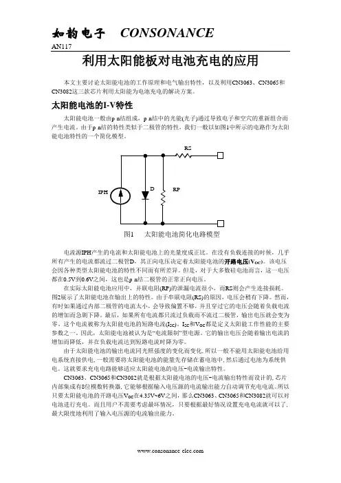
太阳能电池的I-V 特性太阳能电池一般由p-n 结组成,p-n 结中的光能(光子)通过导致电子和空穴的重新组合而产生电流。
由于p-n 结的特性类似于二极管的特性,我们一般以如图1中所示的电路作为太阳能电池特性的一个简化模型。
IPH图1 太阳能电池简化电路模型电流源IPH 产生的电流和太阳能电池上的光量度成正比。
在没有负载连接的时候,几乎所有产生的电流都流过二极管D ,其正向电压决定着太阳能电池的开路电压(V OC )。
该电压会因各种类型太阳能电池的特性不同而有所差异。
但是,对于大多数硅电池而言,这一电压都在0.5V 到0.6V 之间,这也是p-n 结二极管的正常正向电压。
在实际太阳能电池应用中,并联电阻(RP)的泄漏电流很小,而RS 则会产生连接损耗。
图2展示了太阳能电池在输出上的特性。
由于串联电阻(RS)的原因,电压会稍有下降。
然而,有时如果通过内部二极管的电流太小,会导致偏置不够,并且穿过它的电压会随着负载电流的增加而急剧下降。
最后,如果所有电流都只流过负载而不流过二极管,输出电压就会变为零。
这个电流被称为太阳能电池的短路电流(I SC )。
I SC 和V OC 都是定义太阳能工作性能的主要参数之一。
因此,太阳能电池被认为是“电流限制”型电源。
它的输出电压会随着输出电流的增加而降低,并在负载电流达到短路电流时降为零。
由于太阳能电池的输出电流同光照强度的变化而变化,所以一般不能用太阳能电池给用电系统直接供电,一般需要将太阳能电池的能量先存储在蓄电池中,然后通过电池为系统供电。
这就要求充电电路能够适应太阳能电池的电压-电流输出特性。
CN3063、CN3065和CN3082就是根据太阳能电池的电压-电流输出特性而设计的,芯片内部集成有8位模数转换器,它能够根据输入电压源的电流输出能力自动调节充电电流。

摘要本科毕业设计(论文)手机充电器的设计与仿真毕业设计(论文)原创性声明和使用授权说明原创性声明本人郑重承诺:所呈交的毕业设计(论文),是我个人在指导教师的指导下进行的研究工作及取得的成果。
尽我所知,除文中特别加以标注和致谢的地方外,不包含其他人或组织已经发表或公布过的研究成果,也不包含我为获得及其它教育机构的学位或学历而使用过的材料。
对本研究提供过帮助和做出过贡献的个人或集体,均已在文中作了明确的说明并表示了谢意。
作者签名:日期:指导教师签名:日期:使用授权说明本人完全了解大学关于收集、保存、使用毕业设计(论文)的规定,即:按照学校要求提交毕业设计(论文)的印刷本和电子版本;学校有权保存毕业设计(论文)的印刷本和电子版,并提供目录检索与阅览服务;学校可以采用影印、缩印、数字化或其它复制手段保存论文;在不以赢利为目的前提下,学校可以公布论文的部分或全部内容。
摘要作者签名:期:学位论文原创性声明本人郑重声明:所呈交的论文是本人在导师的指导下独立进行研究所取得的研究成果。
除了文中特别加以标注引用的内容外,本论文不包含任何其他个人或集体已经发表或撰写的成果作品。
对本文的研究做出重要贡献的个人和集体,均已在文中以明确方式标明。
本人完全意识到本声明的法律后果由本人承担。
作者签名:日期:年月日学位论文版权使用授权书本学位论文作者完全了解学校有关保留、使用学位论文的规定,同意学校保留并向国家有关部门或机构送交论文的复印件和电子版,允许论文被查阅和借阅。
本人授权大学可以将本学位论文的全部或部分内容编入有关数据库进行检索,可以采用影印、缩印或扫描等复制手段保存和汇编本学位论文。
涉密论文按学校规定处理。
作者签名:日期:年月日导师签名:日期:年月日摘要1.设计(论文)的内容包括:1)封面(按教务处制定的标准封面格式制作)2)原创性声明3)中文摘要(300字左右)、关键词4)外文摘要、关键词5)目次页(附件不统一编入)6)论文主体部分:引言(或绪论)、正文、结论7)参考文献8)致谢9)附录(对论文支持必要时)2.论文字数要求:理工类设计(论文)正文字数不少于1万字(不包括图纸、程序清单等),文科类论文正文字数不少于1.2万字。
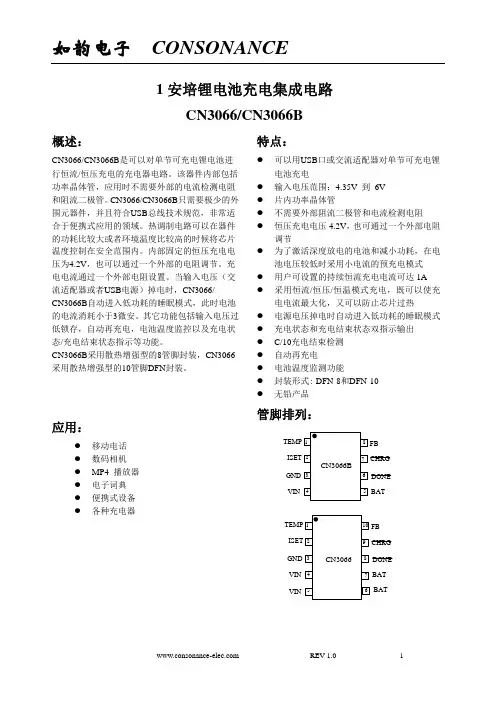
如韵电子CONSONANCE
AN119
充电电流自动调整技术的应用
CN3063/CN3065/CN3082
在实际应用中,经常会遇到一个电子产品需要用两路或两路以上的电源对电池充电的应用,比如,一路电源为电源适配器,另一路电源为USB接口,客户希望这两路电源有任何一路存在时都能为电池充电,电源适配器一般有较强的电流输出能力,可以实现对电池的快速充电;虽然USB接口的输出电流能力比较弱,但因为其随处可用,可以方便地对电池充电。
由于两路电源的输出电流能力不同,导致充电电流的设置陷入两难的境地,如果充电电流根据输出电流能力较强的电源来设置,那么当由较弱输出电流能力的电源供电时,就不能正常充电;反之,如果充电电流根据输出电流能力较弱的电源来设置,那么当由较强输出电流能力的电源供电时,就浪费了该电源的能力,不能实现快速充电。
例如,假设有两路电源,一路为电源适配器,输出电流能力为1安培;另一路为USB接口,其输出电流能力为500毫安,那么如果将充电电流设置在1安培,就不能用USB接口来充电;如果将充电电流设置在500毫安,那么就浪费了电源适配器的能力,不能对电池进行快速充电。
如果用上海如韵电子有限公司的CN3063/CN3065/CN3082就可以很方便地
解决这个问题。
在CN3063/CN3065/CN3082内部集成有8位模拟-数字转换电路,可以根据电源的输出电流能力自动调整充电电流,用户不需要考虑最坏情况,可最大限度地利用输入电源的电流输出能力。
为了解决上面例子的问题,可以使用CN3065,将充电电流设置在1安培,那么当用电源适配器供电时,用1安培的电流向电池充电,当用USB接口供电时,CN3065会自动将充电电流降到500毫安,以适应USB接口的输出电流能力,保证充电能够正常进行。

锂电池转干电池充放管理芯片-概述说明以及解释1.引言1.1 概述概述随着科技的不断发展,电池作为一种常见的电力供应方式,在我们的日常生活中扮演着越来越重要的角色。
传统的锂电池在许多方面都表现出了较好的性能,但是其存在一些使用限制,如充电时间长、容量下降、对温度敏感等问题。
而干电池则具有更长的寿命、更高的能量密度和更好的适应性,因此在某些特定应用领域有着广泛的应用。
为了解决锂电池的使用限制,一种新型的管理芯片问世了——锂电池转干电池充放管理芯片。
这种芯片可以将锂电池的充放电特性转换为符合干电池的需求,从而提供更稳定的供电和更长的使用寿命。
它通过优化充放电过程、合理控制电池的工作温度、降低电池容量衰减等方式,使得电池的性能和稳定性得到了显著提升。
在本文中,我们将会详细介绍锂电池和干电池的特点,并阐述为什么需要将锂电池转换为干电池。
随后,我们将重点介绍锂电池转干电池充放管理芯片的意义、技术要点和应用前景。
通过对这些内容的研究和探讨,我们希望能够更好地理解锂电池转干电池充放管理芯片的工作原理,并展望其在未来的发展趋势。
本文的结论部分将总结锂电池转干电池充放管理芯片的重要意义、技术要点和应用前景,并对其未来发展方向进行展望。
通过这篇文章,读者将能够对锂电池转干电池充放管理芯片有一个更全面和深入的了解,从而更好地应用于相关领域,并推动该技术的进一步发展。
1.2 文章结构本文共分为引言、正文和结论三个部分。
引言部分将介绍本文的概述、文章结构和目的。
首先,我们将概述锂电池和干电池的特点,以及锂电池转干电池的需求。
紧接着,本文旨在介绍锂电池转干电池充放管理芯片的意义、技术要点和应用前景。
正文部分将详细探讨锂电池和干电池的特点。
首先,我们将介绍锂电池的特点,包括其优点和缺点。
其次,我们将探讨干电池的特点,以及与锂电池相比的优势和劣势。
最后,我们将分析锂电池转干电池的需求,包括市场需求和技术需求。
结论部分将总结本文的主要内容。
锂电池充电管理芯片CN3052ACN3052BCN3056性能及应用电路图锂电池充电管理芯片CN3052A/CN3052B/CN3056性能及应用电路图CN3052A/CN3052B/CN3056的主要功能介绍电源低电压检测(UVLO) CN3052A/CN3052B/CN3056内部有电源电压检测电路,当电源电压低于电源电压过低阈值(典型值4.03V)时,芯片处于关断状态,充电也被禁止。
睡眠模式CN3052A/CN3052B/CN3056内部有睡眠状态比较器,当输入电压VIN小于电池端电压+40mV时,充电器处于睡眠模式;只有当输入电压VIN上升到电池端电压90mV以上时,充电器才能离开睡眠模式,进入正常工作状态。
预充电状态在充电周期的开始,如果电池电压低于3V,充电器处于预充电状态,充电器以恒流充电模式充电电流的10%对电池进行充电。
设定充电电流CN3052A/CN3052B/CN3056的恒流模式充电电流可以由ISET管脚的电阻来设定。
充电电流:热调制功能CN3052A/CN3052B/CN3056内部集成有热调制电路,当芯片的温度上升到一定的温度(115℃)后,热调制电路开始动作,将芯片的温度维持在115℃,处于恒温状态。
这项功能对于线性充电器电路非常重要,甚至可以说是必不可少的。
有了这项功能,用户在设计最大充电电流时,只要考虑通常情形就可以了,而不需要考虑最坏工作情况。
如果没有热调制功能,用户在设计最大充电电流时,必须充分考虑最坏情况,否则稍有不慎,芯片将会因为温度过高而被烧毁。
CN3052A/CN3052B/CN3056典型应用电路图CN3052A/CN3052B/CN3056是高性能的线性锂电池充电管理芯片。
这些器件内部集成有功率管,不需要外部的电流检测电阻和阻流二极管,只需要极少的外围元器件,并且符合USB总线技术规范,可以通过USB端口为锂电池充电,因此非常适用于各种充电器及MP4播放器、蓝牙耳机、数码相机等便携式产品。
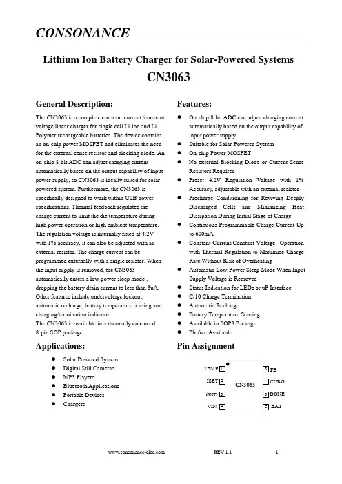
Lithium Ion Battery Charger for Solar-Powered SystemsCN3063General Description:The CN3063 is a complete constant-current /constant voltage linear charger for single cell Li-ion and Li Polymer rechargeable batteries. The device contains an on-chip power MOSFET and eliminates the need for the external sense resistor and blocking diode. An on-chip 8-bit ADC can adjust charging current automatically based on the output capability of input power supply, so CN3063 is ideally suited for solar powered system. Furthermore, the CN3063 is specifically designed to work within USB power specifications. Thermal feedback regulates the charge current to limit the die temperature during high power operation or high ambient temperature. The regulation voltage is internally fixed at 4.2V with 1% accuracy, it can also be adjusted with an external resistor. The charge current can be programmed externally with a single resistor. When the input supply is removed, the CN3063 automatically enters a low power sleep mode , dropping the battery drain current to less than 3uA. Other features include undervoltage lockout, automatic recharge, battery temperature sensing and charging/termination indicator.The CN3063 is available in a thermally enhanced8-pin SOP package.Applications:●Solar Powered System●Digital Still Cameras●MP3 Players●Bluetooth Applications●Portable Devices●Chargers Features:●On-chip 8-bit ADC can adjust charging currentautomatically based on the output capability ofinput power supply●Suitable for Solar-Powered System●On-chip Power MOSFET●No external Blocking Diode or Current SenseResistors Required●Preset 4.2V Regulation V oltage with 1%Accuracy, adjustable with an external resistor●Precharge Conditioning for Reviving DeeplyDischarged Cells and Minimizing Heat Dissipation During Initial Stage of Charge●Continuous Programmable Charge Current Upto 600mA●Constant-Current/Constant-Voltage Operationwith Thermal Regulation to Maximize ChargeRate Without Risk of Overheating●Automatic Low-Power Sleep Mode When InputSupply Voltage is Removed●Status Indication for LEDs or uP Interface●C/10 Charge Termination●Automatic Recharge●Battery Temperature Sensing●Available in SOP8 Package●Pb-free AvailablePin AssignmentFBGNDVIN BATCHRGDONETypical Application CircuitInput Power Supply 4.4V to 6VFigure 1 Typical Application Circuit(Constant V oltage Level 4.2V) Input Power Supply 4.4V to 6VFigure 2 Application Circuit(Adjust Constant V oltage Level with Rx)In Figure 2, the BAT pin’s voltage in constant voltage mode is given by the following equation:Vbat = 4.2+3.04×10⁻⁶×RxWhere,Vbat is in voltRx is in ohmBlock DiagramFigure 3 Block DiagramPin DescriptionPin No. Name Function Description1 TEMPTemperature Sense Input. Connecting TEMP pin to NTC thermistor’soutput in Lithium ion battery pack. If TEMP pin’s voltage is below 46% ofinput supply voltage V IN for more than 0.15S, this means that battery’stemperature is too high or too low, charging is suspended. If TEMP’s voltagelevel is above 46% of input supply voltage for more than 0.15S, battery faultstate is released, and charging will resume.The temperature sense function can be disabled by grounding the TEMP pin.2 ISETConstant Charge Current Setting and Charge Current Monitor Pin. Thecharge current is set by connecting a resistor R ISET from this pin to GND.When in precharge mode, the ISET pin’s voltage is regulated to 0.2V. When inconstant charge current mode, the ISET pin’s voltage is regulated to 2V. In allmodes during charging, the voltage on ISET pin can be used to measure thecharge current as follows:I CH = (V ISET/R ISET)×9003 GNDGround Terminal.4 VINPositive Input Supply Voltage. V IN is the power supply to the internal circuit.When V IN drops to within 40mv of the BAT pin voltage, CN3063 enters lowpower sleep mode, dropping BAT pin’s current to less than 3uA.5 BATBattery Connection Pin. Connect the positive terminal of the battery to BATpin. BAT pin draws less than 3uA current in chip disable mode or in sleepmode. BAT pin provides charge current to the battery and provides regulationvoltage of 4.2V.6Open-Drain Charge termination Status Output. In charge terminationstatus, is pulled low by an internal switch; Otherwise pin is inhigh impedance state.7Open Drain Charge Status Output. When the battery is being charged, thepin is pulled low by an internal switch, otherwise pin is in highimpedance state.8 FBBattery Voltage Kevin Sense Input. This Pin can Kelvin sense the batteryvoltage; Also the regulation voltage in constant voltage mode can be adjustedby connecting an external resistor between FB pin and BAT pin. Absolute Maximum RatingsAll Terminal V oltage……………-0.3V to 6.5V Maximum Junction Temperature…...150℃BAT Short-Circuit Duration………...Continuous Operating Temperature…...-40℃ to 85℃Storage Temperature….............-65℃ to 150℃ Thermal Resistance (SOP8)………….TBDLead Temperature(Soldering)…….............300℃Stresses beyond those listed under ‘Absolute Maximum Ratings’ may cause permanent damage to the device. These are stress ratings only and functional operation of the device at these or any other conditions above those indicated in the operational sections of the specifications is not implied. Exposure to Absolute Maximum Rating Conditions for extended periods may affect device reliability.Electrical Characteristics(VIN=5V, T A=-40℃ to 85℃, Typical Values are measured at T A=25℃,unless otherwise noted) Parameters Symbol TestConditions Min Typ Max Unit Input Supply Voltage VIN 4.4 6 V Operating Current I VIN Charge Termination Mode 400 650 950uA Undervoltage Lockout Vuvlo VIN falling 3.7 3.9V Undervoltage LockoutHysteresisHuvlo 0.1 V Regulation Voltage V REG Constant Voltage Mode 4.158 4.2 4.242 VR ISET=3.6K, V BAT=3.6V 400 500 600R ISET=3.6K, V BAT=2.4V25 50 75mAV BAT=V REG, standby mode 1.75 3.5 7 BAT pin Current I BATVIN=0V, sleep mode 3uA Precharge ThresholdPrecharge Threshold V PRE Voltage at BAT pin rising 2.9 3.0 3.1 VPrecharge Threshold Hysteresis H PRE 0.1VCharge Termination ThresholdCharge TerminationThresholdVterm Measure voltage at ISET pin 0.18 0.22 0.26 V Recharge ThresholdRecharge Threshold V RECH V REG-0.1 V Sleep ModeSleep Mode Threshold V SLP V IN from high to low, measuresthe voltage (V IN-V BAT)40 mvSleep mode Release Threshold V SLPRV IN from low to high, measuresthe voltage (V IN-V BAT)90 mvISET PinPrecharge mode 0.2ISET Pin Voltage V ISETConstant current mode 2.0VTEMP PINInput Threshold V TEMP43.5 46 48.5%V INTEMP input Current TEMP to V IN or to GND 0.5uAPinSink Current I DONE V DONE=0.3V, termination mode 10 mA Leakage Current V DONE=6V, charge mode 1 uAPinSink Current I CHRG V CHRG=0.3V, Charge status 10 mALeakage Current V CHRG=6V, termination mode 1 uADetailed DescriptionThe CN3063 is a linear battery charger designed primarily for charging single cell lithium-ion orlithium-polymer batteries. Featuring an internal P-channel power MOSFET, the charger uses aconstant-current/constant-voltage to charge the batteries. Continuous charge current can be programmed up to 600mA with an external resistor. No blocking diode or sense resistor is required. The on-chip 8-bit ADC can adjust charging current automatically based on the output capability of input power supply, so CN3063 is ideally suited for the solar-powered systems, or the applications that need to charge lithium-ion battery or lithiumpolymer battery with an input power supply whose output capability is limited. The open-drain outputand indicates the charger’s status. The internal thermal regulation circuit reduces the programmed charge current if the die temperature attempts to rise above a preset value of approximately 115℃. This feature protects the CN3063 from excessive temperature, and allows the user to push the limits of the power handling capability of a given circuit board without risk of damaging the CN3063 or the external components. Another benefit of adopting thermal regulation is that charge current can be set according to typical, not worst-case, ambient temperatures for a given application with the assurance that the charger will automatically reduce the current in worst-case conditions.The charge cycle begins when the voltage at the V IN pin rises above the UVLO level, a current set resistor isconnected from the ISET pin to ground. The pin outputs a logic low to indicate that the charge cycle is ongoing. At the beginning of the charge cycle, if the voltage at FB pin is below 3V, the charger is in precharge mode to bring the cell voltage up to a safe level for charging. The charger goes into the fast chargeconstant-current mode once the voltage on the FB pin rises above 3V. In constant current mode, the charge current is set by R ISET. When the battery approaches the regulation voltage, the charge current begins to decrease as the CN3063 enters the constant-voltage mode. When the current drops to charge termination threshold, thecharge cycle is terminated, is pulled low by an internal switch and pin assumes a high impedance state to indicate that the charge cycle is terminated. The charge termination threshold is 10% of the current in constant current mode. To restart the charge cycle, just remove the input voltage and reapply it. The charge cycle can also be automatically restarted if the FB pin voltage falls below the recharge threshold. The on-chip reference voltage, error amplifier and the resistor divider provide regulation voltage with 1% accuracy which can meet the requirement of lithium-ion and lithium polymer batteries. When the input voltage is not present, the charger goes into a sleep mode, dropping battery drain current to less than 3uA. This greatly reduces the current drain on the battery and increases the standby time.The charging profile is shown in the following figure:Charge CurrentBattery VoltageFigure 4 Charging ProfileApplication InformationUndervoltage Lockout (UVLO)An internal undervoltage lockout circuit monitors the input voltage and keeps the charger in shutdown mode until V IN rises above the undervoltage lockout voltage. The UVLO circuit has a built-in hysteresis of 0.1V. Sleep modeThere is an on-chip sleep comparator. The comparator keeps the charger in sleep mode if V IN falls below sleep mode threshold(VBAT+40mv). Once in sleep mode, the charger will not come out of sleep mode until V IN rises 90mv above the battery voltage.Precharge modeAt the beginning of a charge cycle, if the battery voltage is below 3V, the charger goes into precharge mode , and the charge current is 10% of fast charge current in constant current mode.Charging Current limited by the Output capability of Input Power SupplyIf the output capability of input power supply is less than the charging current set by the resistor at ISET pin, then the on-chip 8-bit ADC will begin to function to adjust the charging current based on the output capability of input power supply. In this case, the charging current may be less than the value set by the resistor at ISET pin, but it is maximized to the output capability of input power supply on the condition that the input voltage at VIN pin is no less than 4.35V, which is the minimum operating voltage of CN3063. So the charging current can be set according to the maximum output capability of input power supply, not the worst case.Adjusting the regulation voltage in constant voltage modeThe regulation voltage in constant voltage mode can be adjusted by an external resistor connecting between FB pin and BAT pin as shown in Figure 5:Figure 5 Adjusting Regulation V oltage in Constant V oltage ModeIn Figure 5, the regulation voltage in constant voltage mode will be given by the following equation:Vbat = 4.2+3.04×10⁻⁶×RxWhere,Vbat is in voltRx is in ohmProgramming Charge CurrentThe formula for the battery charge current in constant current mode is:I CH = 1800V / R ISETWhere:I CH is the charge current in ampereR ISET is the total resistance from the ISET pin to ground in ohmFor example, if 500mA charge current is required, calculate:R ISET = 1800V/0.5A = 3.6kΩFor best stability over temperature and time, 1% metal film resistors are recommended. If the charger is in constant-temperature or constant voltage mode, the charge current can be monitored by measuring the ISET pin voltage, and the charge current is calculated as the following equation:I CH = (V ISET / R ISET) × 900Combine Two Power InputsAlthough the CN3063 allows charging from a solar power supply, a wall adapter or a USB port can also be used to charge Li-Ion/Li-polymer batteries. Figure 6 shows an example of how to combine 2 power inputs. AP-channel MOSFET, M1, is used to prevent back conducting into the 2nd power supply when the 1st power supply is present and Schottky diode, D1, is used to prevent 2nd power supply loss through the 1kΩ pull-down resistor.1st power supply supplyFigure 6Combining 2 Input Power SupplyBattery Temperature SenseTo prevent the damage caused by the very high or very low temperature done to the battery pack, the CN3063 continuously senses battery pack temperature by measuring the voltage at TEMP pin.If V TEMP <(46%×VIN) for 0.15 seconds, it indicates that the battery temperature is too high or too low and the charge cycle is suspended. If V TEMP >(46%×VIN) for 0.15 seconds, the charge cycle resumes. The battery temperature sense function can be disabled by connecting TEMP pin to GND.RechargeAfter a charge cycle has terminated, if the battery voltage drops below the recharge threshold of 4.1V, a new charge cycle will begin automatically.Constant-Current/Constant-Voltage/Constant-TemperatureThe CN3063 use a unique architecture to charge a battery in a constant-current, constant-voltage, constant temperature fashion as shown in Figure 3. Amplifiers Iamp, Vamp, and Tamp are used in three separatefeedback loops to force the charger into constant-current, constant-voltage, or constant-temperature mode, respectively. In constant current mode the charge current delivered to the battery equal to 1800V/R ISET . If the power dissipation of the CN3063 results in the junction temperature approaching 115℃, the amplifier Tamp will begin decreasing the charge current to limit the die temperature to approximately 115℃. As the battery voltage rises, the CN3063 either returns to constant-current mode or it enters constant voltage mode straight from constant-temperature mode.Open-Drain Status OutputsThe CN3063 have 2 open-drain status outputs:and . is pulled low when the charger is incharging status, otherwisebecomes high impedance. is pulled low if the charger is in charge termination status, otherwisebecomes high impedance. When the battery is not present, the charger charges the output capacitor to the regulation voltage quickly, then the BAT pin’s voltage decays slowly to recharge threshold because of low leakage current at BAT pin, which results in a 100mv ripple waveform at BAT pin, in the meantime, pin outputs a pulse to indicate that the battery’s absence. The pulse’s frequency is around 10Hz when a 4.7uF output capacitor is used. The open drain status output that is not used should be tied to ground.V IN Bypass Capacitor C INMany types of capacitors can be used for input bypassing, C IN is typically a 22uF capacitor.For the consideration of the bypass capacitor, please refer to the Application Note AN102 from our website.StabilityTypically a 4.7uF capacitor from BAT pin to GND is required to stabilize the feedback loop.In constant current mode, the stability is also affected by the impedance at the ISET pin . With no additional capacitance on the ISET pin, the loop is stable with current set resistors values as high as 50KΩ. However, additional capacitance on ISET pin reduces the maximum allowed current set resistor. The pole frequency at ISET pin should be kept above 200KHz. Therefore, if ISET pin is loaded with a capacitance C, the following equation should be used to calculate the maximum resistance value for R ISET:R ISET < 1/(6.28×2×105×C)In order to measure average charge current or isolate capacitive load from ISET pin, a simple RC filter can be used on ISET pin as shown in Figure 7.Figure 7 Isolating Capacitive Load on ISET PinBoard Layout Considerations1.R ISET at ISET pin should be as close to CN3063 as possible, also the parasitic capacitance at ISET pinshould be kept as small as possible.2.The capacitance at VIN pin and BAT pin should be as close to CN3063 as possible.3.During charging, CN3063’s temperature may be high, the NTC thermistor should be placed far enough toCN3063 so that the thermistor can reflect the battery’s temperature correctly.4.It is very important to use a good thermal PC board layout to maximize charging current. The thermal pathfor the heat generated by the IC is from the die to the copper lead frame through the package lead(especially the ground lead) to the PC board copper, the PC board copper is the heat sink. The footprint copper pads should be as wide as possible and expand out to larger copper areas to spread and dissipate the heat to the surrounding ambient. Feedthrough vias to inner or backside copper layers are also useful in improving the overall thermal performance of the charger. Other heat sources on the board, not related to the charger, must also be considered when designing a PC board layout because they will affect overall temperature rise and the maximum charge current.The ability to deliver maximum charge current under all conditions require that the exposed metal pad on the back side of the CN3063 package be soldered to the PC board ground. Failure to make the thermal contact between the exposed pad on the backside of the package and the copper board will result in larger thermal resistance.Package InformationConsonance does not assume any responsibility for use of any circuitry described. Consonance reserves the right to change the circuitry and specifications without notice at any time.REV 1.1 11。
物联网技术 2022年 / 第1期900 引 言近几年,私家车拥有量快速增加,城市交通压力越来越大,拥堵时间逐步增加,拥堵面积逐年扩大。
经常出现交通拥堵的城市也由一、二线蔓延至三、四线。
交通压力的增加也促进了城市交通建设理念的不断进步,倡导公共交通、提倡绿色出行成为社会共识[1-2]。
在此背景下,越来越多的城市开通并运营了快速公交(BRT )和智轨列车(ART ),提升了城市交通的运行效力[3-4]。
传统交通模式下,通行BRT 和ART 的专用车道禁止社会车辆进入,在没有公交车辆运行的时间,专用车道处于闲置状态,虽保证了通行安全,但也造成了交通资源的浪费[5]。
为了提高专用车道利用率,在保证安全的同时提升交通容量,本文综合了LoRa 和ZigBee 技术,研究了一种可以安全、高效、有序、可靠地引导社会车辆利用公交专用道的路权控制系统[6-8]。
系统支持状态上传,设备维护简便,兼顾安全原则与路权原则,充分考虑到中国交通现状与特点,对解决城市交通拥堵有着积极的探索意义[9-10]。
1 系统架构与作用方式系统由路面信标设备、车载网关设备和后台管理软件 组成。
路面信标沿公交专用车道外侧布置,具有指令接收、状态上传和灯态显示功能。
车载网关设备安装在BRT 或ART 车辆内部,可向信标下发控制命令,接收信标上传的状态信息,通过4G 网络向后台管理软件上传状态参数。
每个发光信标在出厂时设置唯一ID ,所有信标等间距安装,安装时或安装后记录并上传部分信标的GPS 信息至后台管理中心。
其余信标的GPS 信息由后台软件根据信标安装间距自动生成。
信标实行分组管理模式,考虑车辆行驶速度和通信时延,每50 m 内的信标为一组。
每组编号和信标ID 按BRT 行驶方向递增。
BRT 沿公交专用车道行驶时,车载网关以LoRa 模式连续向路面信标发送控制命令,车辆前后一定范围内的信标接收指令并做出响应,控制灯态变化。
BRT 前方300 m范围内信标随车辆行驶依次显示红色灯态,BRT 后方200 m范围内信标随车辆行驶依次显示绿灯。