MIT有机化学讲义
- 格式:pdf
- 大小:3.74 MB
- 文档页数:81
mit化学反应原理MIT化学反应原理MIT(Methyl Isocyanate)是一种有机化合物,它在化学反应中具有重要的作用。
MIT化学反应原理涉及到MIT的生成、转化以及与其他化合物的反应等方面。
本文将从这几个方面来详细介绍MIT化学反应原理。
一、MIT的生成过程MIT的生成通常涉及到异氰酸甲酯(Methyl Isocyanate)和其他化合物之间的反应。
异氰酸甲酯是一种有机化合物,它具有高度的反应性。
在MIT的生成过程中,异氰酸甲酯与一些特定的底物反应,例如甲醇或甲胺。
这些反应通常在高温和高压的条件下进行,以促使反应的进行。
通过控制反应条件和底物的选择,可以有效地合成MIT。
二、MIT的转化过程MIT可以通过多种方式进行转化。
其中一种常见的转化方式是与水反应生成甲酸(Formic Acid)。
这是一个水解反应,通过在MIT中加入适量的水可以促使此反应的进行。
此外,MIT还可以与其他化合物发生加成、取代等反应,生成不同的产物。
这些反应的进行通常需要添加催化剂或调整反应条件,以实现所需的反应路径和产物选择。
三、MIT的反应性MIT是一种具有高度反应性的化合物。
它可以与许多化合物发生反应,包括醇、胺、酸等。
这些反应可以通过调整反应条件和底物的选择来控制。
例如,MIT与醇反应可以生成对应的酯类化合物,而与胺反应则可以生成对应的尿素类化合物。
这些反应的进行可以通过合适的催化剂和反应条件来实现。
四、MIT的应用MIT在化学工业中具有广泛的应用。
它被广泛用于合成各种有机化合物,例如聚氨酯、杀虫剂等。
MIT的高反应性使其在有机合成中成为一种重要的中间体。
通过合理设计反应路径和反应条件,可以利用MIT合成出具有特定结构和性质的化合物。
此外,MIT还被广泛应用于金属表面处理、涂料、塑料等领域。
总结:MIT化学反应原理涉及到MIT的生成、转化以及与其他化合物的反应等方面。
通过合理选择反应底物、调整反应条件以及加入适量的催化剂等手段,可以控制MIT的反应性,从而实现所需的反应路径和产物选择。
mit杀菌剂化学结构MIT杀菌剂是一种常用的杀菌剂,广泛应用于农业生产中。
它的化学结构是什么呢?下面我们来详细介绍一下。
MIT杀菌剂的全称是2-甲基异噁唑-3-醇(2-methyl-1H-isoindole-1,3(2H)-dione)。
它是一种有机化合物,化学式为C4H3NO2,分子量为97.07。
MIT杀菌剂是一种白色结晶固体,无臭,可溶于水。
它具有较强的杀菌作用,对多种病原微生物和真菌有很好的抑制效果。
因此,MIT杀菌剂被广泛应用于农业生产中,用于防治各种作物病害。
MIT杀菌剂的作用机理主要是通过抑制病原微生物和真菌的生长和繁殖来达到杀菌的效果。
它能够干扰病原微生物和真菌的细胞壁合成,破坏其细胞结构,使其不能正常进行代谢和生长。
同时,MIT杀菌剂还能够抑制病原微生物和真菌的酶活性,阻断其代谢途径,从而达到杀灭病原微生物和真菌的目的。
MIT杀菌剂的使用方法一般是将其溶解在水中,然后喷洒在植物叶面或土壤中。
在使用过程中,需要注意控制用药量,避免过量使用,以免对植物产生不良影响。
此外,使用MIT杀菌剂时还需要注意安全防护措施,避免接触皮肤和眼睛。
MIT杀菌剂是一种高效、低毒、广谱的杀菌剂,对多种病原微生物和真菌具有良好的抑制效果。
它在农业生产中的应用广泛,可以有效预防和控制作物病害,提高作物产量和质量。
同时,由于其低毒性和环境友好性,MIT杀菌剂也被广泛应用于食品加工和医药领域。
总之,MIT杀菌剂是一种重要的杀菌剂,具有良好的杀菌效果和安全性。
它的化学结构为2-甲基异噁唑-3-醇,通过抑制病原微生物和真菌的生长和繁殖来达到杀菌的效果。
在农业生产中的应用广泛,并且在食品加工和医药领域也有重要的应用价值。
高二化学有机物推断及知识点总结对于有机推断题首先要熟悉各种官能团的性质,其次对各类有机反应的条件要记牢。
解答有机推断题的常用方法有:1.根据物质的性质推断官能团,如:能使溴水反应而褪色的物质含碳碳双双键、三键“-CHO”和酚羟基;能发生银镜反应的物质含有“-CHO”;能与钠发生置换反应的物质含有“-OH”;能分别与碳酸氢钠镕液和碳酸钠溶液反应的物质含有“-COOH”;能水解产生醇和羧酸的物质是酯等。
2.根据性质和有关数据推知官能团个数,如:-CHO→2Ag→Cu20;2-0H→H2;2-COOH(CO32-)→CO23.根据某些反应的产物推知官能团的位置,如:(1)由醇氧化得醛或羧酸,-OH一定连接在有2个氢原子的碳原子上;由醇氧化得酮,-OH接在只有一个氢原子的碳原子上。
(2)由消去反应产物可确定“-OH”或“-X”的位置。
(3)由取代产物的种数可确定碳链结构。
(4)由加氢后碳的骨架,可确定“C=C”或“C≡C”的位置。
能力点击:以一些典型的烃类衍生物(溴乙烷、乙醇、乙酸、乙醛、乙酸乙酯、脂肪酸、甘油酯、多羟基醛酮、氨基酸等)为例,了解官能团在有机物中的作用.掌握各主要官能团的性质和主要化学反应,并能结合同系列原理加以应用.注意:烃的衍生物是中学有机化学的核心内容,在各类烃的衍生物中,以含氧衍生物为重点.教材在介绍每一种代表物时,一般先介绍物质的分子结构,然后联系分子结构讨论其性质、用途和制法等.在学习这一章时首先掌握同类衍生物的组成、结构特点(官能团)和它们的化学性质,在此基础上要注意各类官能团之间的衍变关系,熟悉官能团的引入和转化的方法,能选择适宜的反应条件和反应途径合成有机物.有机化学知识点总结1.需水浴加热的反应有:(1)、银镜反应(2)、乙酸乙酯的水解(3)苯的硝化(4)糖的水解(5)、酚醛树脂的制取(6)固体溶解度的测定凡是在不高于100℃的条件下反应,均可用水浴加热,其优点:温度变化平稳,不会大起大落,有利于反应的进行。
and two others with nodes (antibonding states), i.e., three molecular orbitals in all. (See fig. 3.)As the length of the chain is increased, the number of electronic states into which the atomic 2s state splits also increases, the number of states always equaling the number of atoms. The same occurs when lithium chains are placed side-by-side or stacked on top of each other, so that finally the space lattice of the lithium crystal is obtained. It is of great significance that these electronic states have energies which are bounded by an upper and lower limiting value (see fig. 4). Within these limits the states form an energy band of closely spaced values (one gram of lithium contains nearly 1023 atoms). Similarly, energy bands can also result from overlapping p and d orbitals. The electronic states (orbitals) within an energy band are filled progressively by pairs of electrons in the same way that the orbitals of an atom were filled in accordance with the Pauli principle. This means that for lithium the electronic states of the 2s band will be exactly half-filled.It is of interest to consider why lithium atoms or Li2 molecules combine to form a metal lattice. In the lithium lattice the smallest distance between neighboring atoms is3.03 x 10–10 m, which is larger than in the Li2 molecule. This reflects the fact that bonds between pairs of atoms in the metal are weaker than they are in the molecule. Nevertheless, the metallic form of lithium is more stable than the molecular form because in the metal one atom has many more neighbors than in the Li2 molecule. As a result, the binding energy per gram atom of lithium (i.e., per 6.92 g of lithium) is163 kJ for the metal lattice, but only 56 kJ for one mole of molecule.[The possibility of hybridization (first advanced by L. Pauling to explain metallic bonding) is also a likely factor for the formation of metallic bonds. Thus strong bonds can be formed when the valence electron clouds become concentrated along the direction in which the bonding partners are situated. According to Pauling the situationtable, can often replace each other in arbitrary proportions without altering either the lattice type or the structure of the energy bands. This explains why such metals tend to form a complete series of solid solutions. Metallic alloys consist of such solid solutions or of heterogeneous mixtures of such solutions. Within certain limits, even metal atoms of different valence can be interchanged in a lattice.Band Structure of MetalsAccording to the above considerations the band structure of Li metal can be represented as shown in fig. 5.According to previous reasoning, the 2s band has N states (N = number of atoms) and accommodates n 2s electrons (where n is the number of electrons per atom in the 2s state times N). Thus, this band has only half of the states filled since each state can accommodate two electrons of opposite spin (Pauli exclusion principle). In accordance with the Aufbau principle, the lowest energy states of the band are filled first and the upper states remain empty – but can readily be occupied by electrons upon thermal excitation or the application of an electric field. Since the width of the energy band is of the order of a few volts, spacings of states within the band are of the order of~10–20 eV (1 eV = 1.6 x 10⁻¹⁹ J), electrons can readily acquire the energy necessary to move into excited states, be accelerated, and move through the metal as conducting electrons. Partly filled bands thus constitute conduction bands.The conduction mechanism in Mg, for example, appears complicated by the fact that each 3s state of the valence shell in the atoms is doubly occupied (3s2). Thus the 3s band must be filled completely and no electronic conduction would in principle be expected. Electronic conduction, however, is observed because of a partial overlap of the 3s and the empty 3p bands. With this overlap, electrons can be activated into empty 3p states and exhibit conduction, as in the partly filled s band in Li.filledsolidfilled levelsFig. 6 Band structure of insulators and semiconductors (molecular crystals); the conditions depicted reflect a molar crystal of carbon (diamond).Both insulators and semiconductors have the same basic band structure – the primary) between the valence and the, generically, are materials with very high resistivity (see T able I), comprising glasses, polymers, refractories, composites, liquids and gases. In the present context, an insulator is a molecular crystal, such as diamond (C) or sapphire, with a band gap ) in excess of 4 eV (arbitrary value). Generally such materials will not conduct electricity since their valence band is filled and the energy required to transfer electronsfrom the valence band to the empty conduction band is far in excess of both the thermal energies at room temperature and the energy provided by radiation of the visible spectrum (~2 eV). Therefore, insulators (in single crystal form) are normally transparent (colorless); however, if light is excessively or totally scattered at internal heterogeneities (such as grain boundaries), they may be translucent and even opaque. It should also be recognized that impurities (Cr3+ in Al2O3) or particular point defects (color centers) may impart a color to the transparent insulator crystals. The color arises because of partial absorption of white light and selective transmission of the other portions of the visible spectrum.Semiconductors: The conventional semiconductors, silicon (Si) and germanium (Ge), have a band gap (E g) of 1.1 and 0.7 eV respectively and therefore absorb visible radiation; they are opaque (fig. 7). Considering the statistical nature of the thermal energy distribution in the solid matrix (Maxwell-Boltzmann), a significant number of electrons in the valence band will, at room temperature, acquire sufficient energy to cross the existing energy gap and thus provide for semiconductivity. The conductivity will therefore increase with temperature, contrary to metallic systems, until electron scattering effects, due to increased lattice vibrations (which decrease the mobility of electrons), begin to dominate.The value of semiconductors for solid state device fabrication lies in the fact that the number and type of conducting electric charge carriers [electrons are n-type (negative), holes are p-type (positive)] can be controlled through incorporation of appropriate dopant elements. Thus the substitutional incorporation of Group V elements (Sb, As, P) provides for shallow donor levels in the band gap at about 0.01 eV from the conduction band. The substitutional incorporation of Group III elements (B, Al) generates acceptor levels in the band gap at about 0.01 eV from the valence band. The two types of impurities are almost completely ionized at room temperature and give rise to extrinsicE h (transparent to light)Insulators (carbon)Impurity and defect levels in the energygap may give rise to selective absorptionof light (colour the object).E h (visible light is absorbed)(-)(+)excited electron holeSemiconductor (Si)Fig. 7 Optical bebavior of insulators and semiconductorsn-type and p-type conductivity – the basis for the formation of diodes and transistors (fig. 8).Of increasing importance are compound GaAs, InSb, InP and GaP (compounds of Group III and Group V elements). Together these compounds provide eight valence electrons and, by sp form a diamond-like, covalent crystal structure with semiconductor properties. These* * * * * * * * * * * * * * * * * * * * * * * * * * * * * * * * * * * * * * * * * * * * * * * *Table I. ELECTRICAL RESISTIVITIES OFMETALS AND NONMETALS AT 20_C*______________________________________________________________________________Resistivity,Resistivity, Metals10–8 ohm–m**Nonmetals ohm–m**______________________________________________________________________________Silver 1.6SemiconductorsCopper 1.67Silicon1000.0Gold 2.3Germanium0.09Aluminum 2.69InsulatorsMagnesium 4.4Diamond1010–1011Sodium 4.61Quartz 1.2 x 10¹²Tungsten 5.5Ebonite 2 x 10¹³Zinc 5.92Sulfur 4 x 10¹³Cobalt 6.24Mica9 x 1013Nickel 6.84Selenium 2 x 10¹⁴Cadmium7.4Paraffin wax 3 x 10¹⁶Iron9.71Tin12.8Lead20.6Uranium29Zirconium41Manganin44Titanium55Lanthanum5996%Iron–4%Si62Cerium78Nichrome100*From American Institute of Physics Handbook, Dwight E. Gray, ed. McGraw-Hill, New York(1963), pp. 4–90; 9–38.**Note the different units in the two columns.* * * * * * * * * * * * * * * * * * * * * * * * * * * * * * * * * * * * * * * * * * * * * * * *EXERCISE FOR THE IDLE MIND1. A solid is found to have an energy band gap (E g) of 3 eV. What is the likely colorof this solid in transmitted sunlight?2.An optically transparent solid appears green in transmitted sunlight. What do youexpect the band gap (E g) of this solid to be (in eV)?3.AlN and GaSb are compounds, solid at room temperature. On the basis ofbonding considerations and data provided in the P/T, attempt to predictdifferences in the properties of these solids.4.Account for the conductivity of (a) Na (metallic) and (b) Mg (metallic) on the basisof appropriate energy diagrams.5.What is the radiation of longest wavelength which is still capable of beingtransmitted through:(a)Si with E g = 1.1 eV(b)Ge with E g = 0.7 eV, and(c)the compound GaAs with E g = 1.43 eV?6.Explain the difference between extrinsic and intrinsic semiconductors.7.Semiconductors in single crystal form are usually produced by solidification ofmelts. To achieve extrinsic semiconductivity it is customary to add to the melt“doping elements” which are substitutionally incorporated [replace, for example, a silicon atom in the crystal (ordered structure)]. If the doping element is P, which has 5 valence electrons, and it replaces a silicon atom (whose 4 valence electrons are normally immobilized because of bond formation), each P atom will be able to contribute one electron to conduction; its other four valence electrons take part in bond formation. Assume you add 3 mg P to 50 g silicon and form a crystal from it in which the P atoms are uniformly distributed; what is the number of conduction electrons/cm3 in the doped crystal? (You may neglect the volume of thesubstitutionally replaced Si atoms and assume that only electrons from P atoms contribute to conduction.)8.Potassium (K) and beryllium (Be) are metals which exhibit good electricalconductivity. Explain for both elements the reasons for the observed conductivity on the basis of the band structure.9.The energy gap (E g) in zinc oxide (ZnO) is 3.2 eV.(a)Is this material transparent to visible radiation?(b)Do you expect this material to be a conductor at room temperature? (Givethe reasons for your answer.)18. A chemical analysis indicates that a silicon crystal weighing 100 g contains 33 mgof aluminum (Al) which is substitutionally incorporated (the Al atoms replace some Si atoms in the crystal).(a)Is this crystal n-type or p-type? (Explain in one sentence.)(b)What is the number of extrinsic charge carriers (per cm3) in this crystal?19.An unknown material is transparent to light of frequencies ($) up to 1.3 x 10¹⁴ s–1.Draw a meaningful schematic band structure for this material.20.We know that, in semiconductors, charge carriers can be thermally activated fromthe valence band into the conduction band. The number of thermally activatedelectrons (n e) per cm3 is given by:n e+A T3ń2e*E gńkT(where A = 5 x 1015 cm–3 for silicon). Determine for pure silicon (Si) the number of electrons/cm3 in the conduction band at 500°C.21. A crystal of germanium (E g = 0.7 eV) is found to be n-type with 5 x 10¹⁸ mobilecharge carriers/cm3 (at room temperature).(a)Draw a schematic energy band diagram that reflects the indicatedproperties. (Label pertinent features in the diagram.)(b)Do you expect this crystal to be transparent or opaque to radiation of $=1 x 10¹⁵ s–1?22.Draw three energy band structures representing respectively (and identifiably) an:(1)extrinsic n-type semiconductor(2)an insulator(3)and a metal.23. A 50 kWatt radio transmitter emits radio waves with a wavelength of 300m. Howmany photons does it emit per minute (1 Joule = 1 Watt per sec)?24. A material exhibits an “optical band edge” (transition from absorption of light totransmission) at $ = 5 x 10¹⁴ Hz (s–).(a)Draw a diagram which reflects the indicated optical behavior.(b)What do you expect the color of this material to be when viewed in daylight?(c)What is the band gap (E g) of this material?25. A sample of germanium (Ge), weighing 30 g, is found to contain 54 mg of arsenic(As). Determine for this sample the mobile charge carrier density (carriers/cm3) at room temperature. (Assume As to be substitutionally incorporated in Ge and that all As atoms are ionized at room temperature; you may neglect any intrinsiccharge contributions.)。
target material and result in electronic excitation. If the energy of the arriving electrons is high enough, some may knock out a K shell electron in the target and thus generate a vacancy. [It should be clear that a K # L excitation cannot take place since the L shell is filled: excitation must involve (n = 1) # (n = $).] When such a vacancy is generated, it can readily be filled by an electron from the L shell or the M shell of the same atom. These internal electron transitions give rise to the emission of “characteristic”X-radiation which, because of its short wavelength, has extremely high “penetrating”power. [Since an electron beam is used to generate X-rays, the X-ray tube has to be evacuated: to dissipate the energy flux arriving at the target, the anode support (onto which the target is mounted) is water-cooled.]Under standard operating conditions, the characteristic radiation emitted by the target comprises two sharp lines, referred to as K" and K% lines (fig. 3). They are associated, respectively, with electron transitions from n = 2 to n = 1 and from n = 3 to n = 1.Emitted X-ray spectra were extensively studied by H.G.J. Moseley who established the relationship between the wavelength of characteristic radiation and the atomic number Z of the radiation emitting target material (fig. 4). Experimentally he found that the K" lines for various target materials (elements) exhibit the relationship:(n K a T Z2)l K a T1Z2Moseley’s empirical relationship (which reflects a behavior in agreement with the Rydberg equation) can be quantified. While the energy levels associated with outer electron transitions are significantly affected by the “screening” effect of inner electrons (which is variable and cannot as yet be determined from first principles), the conditions associated with X-ray generation are simple. Very generally, the screening effect of the innermost electrons on the nuclear charge is accounted for in an effective nuclearShortest Wavelength (SWL) – the cut-off of the continuous spectrum for decreasing values of & (fig. 5). Analytically, we have:;l SWL+hc eVeV+h n max+h c lSWLFrom this relationship it is evident that the cut-off of the continuous spectrum toward decreasing &’s (&SWL) is controlled by the accelerating potential (fig. 5).3.THE “FINE STRUCTURE” OF CHARACTERISTIC X-RAYSIt is customary to consider the characteristic X-ray spectral lines as discrete lines (K", K%, L", L%, etc.). In reality, they are not discrete since the electron shells involved in the associated electron transitions have energy sublevels (s, p, d orbitals). These sublevels give rise to a “fine structure” insofar as the K" lines are doublets composed of K"1 and K"2 lines. Similarly, L", L%, etc., exhibit a fine structure.These considerations suggest that X-ray spectra contain information concerning the energetics of electronic states. Obviously, analysis of X-rays emitted from a target of unknown composition can be used for a quantitative chemical analysis. [This approach is taken routinely in advanced scanning electron microscopy (SEM) where X-rays, generated by the focused electron-beam, are analyzed in an appropriate spectrometer.] In fundamental studies it is also of interest to analyze soft (long &) X-ray spectra. For example, take the generation of X-rays in sodium (Na). By generating an electron vacancy in the K shell, a series of K" and K% lines will result. The cascading electron generates vacancies in the 2p level, which in turn can be filled by electrons entering from the 3s level (generation of “soft” X-rays). If the X-rays are generated in a Na vapor, the 3s # 2p transition will yield a sharp line; on the other hand, if X-rays are analyzed in sodium metal, the same transition results in the emission of a continuous broad band, about 30 Å in width. This finding confirms the existence of an energy band (discussed earlier).fact that all reflections present have unmixed indices indicates that the Bravais lattice is FCC – the extra missing reflections give additional information as to the exact atom arrangement.)A hypothetical diffraction experiment: A material is known to be of simple cubic structure; determine a, the lattice constant, by X-ray diffraction. In theory, the question may be answered by placing the crystal into a diffractometer, rotating it into all possible positions relative to the incident X-ray beam and recording all diffracting 2+ values. From the above we know that the smallest observed + value must correspond to diffraction on {100} planes and also that d(100) = a. We may now use Bragg’s equation to determine a, the lattice constant:l+2d sin q+2a sin qa+l2sin qThere are two simplifying assumptions in this problem: (1) we know the system is SC and (2) we are able, through rotation, to bring all planes present into diffraction conditions.6.EXPERIMENTAL APPROACHES TO X-RAY DIFFRACTIONIn the context of this course we are interested in making use of X-ray diffraction for the purpose of (a) identifying (cubic) crystal systems, (b) determining the lattice constant, a, and (c) identifying particular planes or meaningful orientations. The possible approaches can, in principle, be identified through an examination of Bragg’s law. The Bragg condition for particular d(hkl) values can be satisfied by adjusting either one of two experimental variables: (a) &, the wavelength of the X-ray beam used, or (b) +, the orientation of the crystal planes relative to the incident X-rays.sin2q (h2)k2)l2)+l24a2+const.Substitution and rearrangement of above yields:Accordingly, we find that for all lines (+ values) of a given pattern, the relationshipsin2q1 (h2)k2)l2)1+sin2q2(h2)k2)l2)2+sin2q3(h2)k2)l2)3+const.holds. Since the sum (h2 + k2 + l2) is always integral and &2/4a2 is a constant, the problem of indexing the pattern of a cubic system is one of finding a set of integers(h2 + k2 + l2) which will yield a constant quotient when divided one by one into the observed sin2+ values. (Certain integers such as 7, 15, 23, etc. are impossible because they cannot be formed by the sum of three squared integers.)Indexing in step-by-step sequence is thus performed as follows: + values of the lines are obtained from the geometric relationship of the unrolled film strip. Between the exit hole of the X-ray beam (2+ = 0_) and the entrance hole (2+ = 180_) the angular relationship is linear (fig. 12). The increasing + values for successive lines are indexed +1, +2,+3, etc., and sin2+ is determined for each. If the system is simple cubic we know that all planes present will lead to diffraction and the successive lines (increasing +) result from diffraction on planes with decreasing interplanar spacing: (100), (110), (111), (200), (210), (211), (220), etc. From equation (3) above we recognize:sin2q11+sin2q22+sin2q33+sin2q44+sin2q55+const.If the system is BCC, however, we know from the selection rules that only planes for which (h + k + l) = even will reflect. Thus:sin2q12+sin2q2+sin2q3+sin2q4etc.+const.[SC can be differentiated from BCC through the fact that no sum of three squared integers can yield 7, but 14 can be obtained from planes (321)].For FCC systems, the selection rules indicate reflections on planes with unmixed h,k,l indices:sin2q13+sin2q24+sin2q38++const.After proper indexing, the constant is obtained:sin2q(h2)k2)l2)+const.and the particular Bravais lattice is identified. The lattice constant of the unit cell is subsequently obtained, knowing the wavelength of the incident radiation:sin2q (h2)k2)l2)+const.+l24a2a2+l24sin2q(h2)k2)l2) a+l(h2)k2)l2)ǸEXERCISE FOR THE IDLE MIND1.(a)Give a schematic drawing of the X-ray spectrum emitted from a molybdenum(Mo) target and identify on it with appropriate symbols all characteristicwavelengths.(b)Explain the origin of all characteristic “&’s” on a schematic drawing and anenergy diagram respectively.(c)Assuming the X-ray unit is operated with an accelerating voltage of 40 kV,what is the shortest X-ray wavelength (&) obtained from it?2. A powder of a material, crystallizing in a BCC structure (a = 10 x 10–10 m), isexposed to the radiation emitted from an X-ray tube operated at a voltage (V).Below which value of V will no wavelength emitted by the X-ray tube be able to cause diffraction?3.For an unknown cubic metal the diffracting angles, +, obtained with CuK" radiation(& = 1.541 Å) are: 20.1°, 29.2°, 36.6°, 43.5°, 50.2°, 57.4°, 65.5°.(a)Determine the lattice constant “a” for this metal.(b)Determine the atomic radius for this metal.4.Calculate the angular position of the first diffraction peak (smallest +) for Cr andfor Pd using CuK" radiation (& = 1.542 Å).5.Gold (Au) is studied in a Debye-Scherrer diffraction arrangement. Using radiationof 1 Å, what is the diffraction angle (+) for (a) the (112) planes and (b) the (220) planes?6.An X-ray generator operates with a deficient power supply which can only deliveran accelerating voltage of kV.(a)Will you be able to obtain CuK" radiation (& = 1.542 Å) from this generator?(b)What is the shortest & of X-radiation obtainable?(c)Assuming the shortest & obtainable through Bremsstrahlung (&SWL) were1.380 Å, which is the same wavelength as that of CuK%, could CuK"radiation be obtained under these conditions?7.From a hypothetical diffraction experiment involving a “cubic” crystal, the followingsin2+ values are obtained: 0.100, 0.200, 0.300, 0.400, 0.500, 0.600, 0.800 and0.900. Is this system SC, BCC or FCC? Attempt to find the answer by deductivereasoning along; after writing down the answer, explain how you arrived at your conclusion.8.An element of BCC structure crystallizes with a lattice constant (a) of 3.26 Å. Whatis the minimum acceleration potential that must be applied to an X-ray generator so as to still observe in this material X-ray diffraction with radiation emanatingfrom this tube?9.What will be the Miller indices for the smallest diffracting angles (with a given fixed&) for:(a)SC crystals?(b)FCC crystals?(c)BCC crystals?10.On a crystal (cubic) a set of diffraction lines (+) was obtained with CuK" (1.54 Å)radiation: 13.70, 15.89, 22.75, 26.91, 28.25, 33.15, 36.62, 37.60 and 41.95degrees. What is the lattice parameter of this solid?ing CuK" radiation in a diffraction experiment on Ag, what are the values of thethree smallest +angles?12.What is the smallest acceleration potential that must be applied to an X-raygenerator so as to still achieve diffraction in solid potassium (at roomtemperature)?13.For a diffraction experiment on gold (Au) a collimated beam of electrons, ratherthan X-rays, is used. Assuming the acceleration potential (V) for the electron is45 kV, what will be the Bragg angle, +, for (220) diffraction?ing K" radiation of vanadium (V) in a diffraction experiment on an unknowncubic (BCC) material, the first diffraction peak is observed at 2+ = 83.5°. What is the lattice constant (a) of this material?15.The interplanar spacing of the {110} planes in an iron (Fe) crystal is 2.024 Å. Atthat Bragg angle (+) will AgK" radiation experience first order diffraction (alsocalled reflection) on these planes?16.An X-ray generator with an unknown target material yields K" radiation with whichthe smallest diffraction peak (2+1) in tantalum (Ta) is found to be at 58.7°. What is the target material in the X-ray generator?17.On a Debye-Scherrer film strip, after exposure to diffraction from a face-centeredcubic Ni specimen, the separation between the two lines lying closest to theposition of the undiffracted (transmitted) beam is 7.8 cm.(a)What planes of the crystal structure are responsible for these lines?(b)Knowing that the radius of the camera is 5 cm and that CuK" radiation isused in this experiment, determine the atomic radius of Ni.ing electrons accelerated by 100,000 Volt, what will be + (the diffraction angle)for diffraction on (112) planes in gold (Au)?19.The Debye-Scherrer pattern of an unknown material exhibits reflections(diffraction peaks) at 40.50°, 58.60°, 73.64°, 87.62°, 101.38°, 116° and 132.6°,using CuK" radiation (& = 1.541 Å). Determine the molar volume of this material.20.Diffraction experiments on Ag are made at 300K and at 1073K with MoK"radiation (& = 0.709 Å). It is found that the diffraction angle +(111) at 1073K is by0.11° smaller than that at 300K. Determine the molar volume of Ag at 800°C. (Youmay make use of information in your Periodic T able.)21.In an unknown material of cubic structure, (100) diffraction is obtained at 14.88°with radiation of & = 1.541 Å. Can this material accommodate interstitially (in void space) atoms of 1.08 Å radius without lattice distortion?22. A powder of a metallic system with BCC structure and a lattice constant of 5.5 Å isexposed to the radiation from an X-ray tube operated at 1.2 kV. How manydiffraction cones can be generated by this powder in a Debye-Scherrer set-up.23.You are given an unknown material of irregular shape and are asked to determine(a) if the material is crystalline, (b) if it belongs to the BCC system, and (c) thelattice constant of its unit cell. How would you proceed? (Give your answer in no more than ten lines with no more than three equations.)24. A powder of an FCC system with a lattice constant (a) of 6 Å is exposed toradiation emitted from an X-ray tube operated at an accelerating potential (V) of1.5 kV (the target material is Cr). How many diffraction cones can the radiationemitted generate in a Debye-Scherrer set-up?25.Do you expect the first diffraction peak in Pd to be shifted to a larger or smaller +value (operating with K", monochromatic X-rays) if you change the target in anX-ray tube from Cu to Mo? Explain.26.Determine the longest wavelength of X-rays which can still produce diffraction invanadium (V).27.Determine the wavelength of &K" for Mo.28.Identify the element giving rise to K" with & = 2.51 x 10⁻¹⁰ m.29.Determine the longest wavelength of radiation that is still capable of producingdiffraction in nickel (Ni).30.You are operating an X-ray tube with an Mo target by applying an accelerationpotential of 50 keV. Draw a schematic of the X-ray spectrum emitted by this tube;label on it three (3) characteristic wavelengths (&’s) and give the calculatednumerical value for two of these.31.When doing “electron diffraction”, what acceleration potential must be applied to abeam of electrons to achieve with them diffraction on {111} planes of gold at +=6°?32.Determine the smallest acceleration potential that must be applied in an X-raygenerator so as to still achieve diffraction in nickel (Ni).33.An element, solid, of BCC structure has the lattice constant 0.316 nm with adensity of 19.3 g/cm3. Calculate the atomic weight of this element.34.Draw the schematic of a set-up for an X-ray diffractometer experiment on ironusing NiK" radiation. (Provide as much information as required to achievemonochromatic K" radiation suitable for the diffraction study.)35.Determine the chemical element that will generate K" radiation with an energy of7.725 x 108 J/mole photons.36.At what Bragg angle (+) will K" radiation from a Ni target experience first orderdiffraction on {110} planes of BCC iron?37.Give a definition for the “unit cell”.38.What is the coordination number of each atom in (a) a three-dimensional,close-packed array of equal sized spheres, (b) a simple cubic structure and (c) a body centered cubic lattice?39.Describe what is understood by “constructive interference” and “destructiveinterference” and explain how these terms apply to the diffraction of X-rays by a crystal.40.Explain the fact that a polycrystalline (fine grained) aluminum sample exhibits ahigher tensile strength (strength under tension) than a high quality Al singlecrystal.。
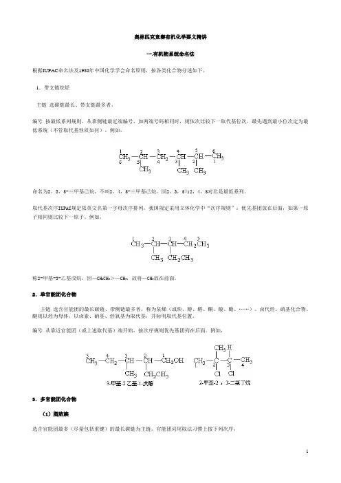
奥林匹克竞赛有机化学要义精讲一.有机物系统命名法根据IUPAC命名法及1980年中国化学学会命名原则,按各类化合物分述如下。
1.带支链烷烃主链选碳链最长、带支链最多者。
编号按最低系列规则。
从靠侧链最近端编号,如两端号码相同时,则依次比较下一取代基位次,最先遇到最小位次定为最低系统(不管取代基性质如何)。
例如,命名为2,3,5-三甲基己烷,不叫2,4,5-三甲基己烷,因2,3,5与2,4,5对比是最低系列。
取代基次序IUPAC规定依英文名第一字母次序排列。
我国规定采用立体化学中“次序规则”:优先基团放在后面,如第一原子相同则比较下一原子。
例如,称2-甲基-3-乙基戊烷,因—CH2CH3>—CH3,故将—CH3放在前面。
2.单官能团化合物主链选含官能团的最长碳链、带侧链最多者,称为某烯(或炔、醇、醛、酮、酸、酯、……)。
卤代烃、硝基化合物、醚则以烃为母体,以卤素、硝基、烃氧基为取代基,并标明取代基位置。
编号从靠近官能团(或上述取代基)端开始,按次序规则优先基团列在后面。
例如,3.多官能团化合物(1)脂肪族选含官能团最多(尽量包括重键)的最长碳链为主链。
官能团词尾取法习惯上按下列次序,—OH>—NH2(=NH)>C≡C>C=C如烯、炔处在相同位次时则给双键以最低编号。
例如,(2)脂环族、芳香族如侧链简单,选环作母体;如取代基复杂,取碳链作主链。
例如:(3)杂环从杂原子开始编号,有多种杂原子时,按O、S、N、P顺序编号。
例如:4.顺反异构体(1)顺反命名法环状化合物用顺、反表示。
相同或相似的原子或基因处于同侧称为顺式,处于异侧称为反式。
例如,(2)Z,E命名法化合物中含有双键时用Z、E表示。
按“次序规则”比较双键原子所连基团大小,较大基团处于同侧称为Z,处于异侧称为E。
次序规则是:(Ⅰ)原子序数大的优先,如I>Br>Cl>S>P>F>O>N>C>H,未共享电子对:为最小;(Ⅱ)同位素质量高的优先,如D>H;(Ⅲ)二个基团中第一个原子相同时,依次比较第二、第三个原子;(Ⅳ)重键分别可看作(Ⅴ)Z优先于 E,R优先于S。
高中有机化学知识必备讲义中学有机化学“断键”全解一.取代反应1.卤代反应:C—H键断裂①烷烃的卤代:CH4 + Cl2 CH3Cl + HCl反应条件:光照、纯卤素②苯的卤代:反应条件:液溴、催化剂(FeBr3) ③苯的同系物的卤代:反应条件:液溴、催化剂(FeBr3)④酚的卤代:反应条件:浓溴水⑤醇的卤代:C2H5O H + HBr C2H5Br + H2O反应条件:浓硫酸作催化剂、脱水剂,加热2.硝化反应:C—H键断裂①苯的硝化反应条件:浓硫酸作催化剂、脱水剂,水浴加热55—60℃②苯的同系物的硝化反应条件:浓硫酸作催化剂、脱水剂,加热③酚的硝化反应条件:浓硫酸作催化剂、脱水剂3.酯化反应:羧酸中的C—O键、醇中的O—H键断裂CH3C OO H + C2H5OH CH3C OO CH2CH3 + H2O反应条件:浓硫酸作催化剂、脱水剂,加热4.水解反应①卤代烃的水解:C—X断裂C2H5Br + H2O C2H5OH + HBr反应条件:强碱NaOH的水溶液,加热②酯的水解:C—O键断裂反应条件:稀硫酸作催化剂,水浴加热70—80℃③蛋白质的水解:酰氨键中C—N键断裂5.醇与醇分子间脱水:醇分子中的的C—O键与另一醇分子中与羟基相连碳原子上的C—H键发生断裂2 CH3CH2OH CH3CH2OCH2CH3 + H2O反应条件:浓硫酸作催化剂、脱水剂,加热140℃6.置换反应:①醇的置换反应:O—H键断裂2 CH3CH2OH + 2 Na →2CH3CH2ONa + H2↑反应条件:活泼金属(K、Ca、Na、Mg、Al、Li等)②酚的置换反应:O—H键断裂反应条件:活泼金属(K、Ca、Na、Mg、Al、Li等),熔化的苯酚③羧酸的置换反应:O—H键断裂2CH3COOH + Zn →(CH3COO)2Zn + H2↑反应条件:氢以前的活泼金属7.羧酸盐的脱羧反应:C—C键断裂CH3C OO Na + Na O H CH4↑+ Na2CO3反应条件:羧酸盐无水,加热8.复分解反应:C—H键断裂①中和反应:R COOH + NaOH → R COONa + H2O②羧基的检验:R COOH + NaHCO3→ R COONa + H2O + CO2↑二.加成反应1.烯烃的加成反应:断裂中的一个键①与水的加成:CH2=CH2 + H2O CH3CH2OH②与卤素的加成:CH2=CH2 + Br2 → CH2BrCH2Br③与卤代烃的加成:CH2=CH2 + HCl CH3CH2Cl④与氢气的加成:CH2=CH2 + H2 CH3CH32.炔烃:断裂中的一个键或二个键①与水的加成:②与卤素的加成:③与卤代烃的加成:④与氢气的加成:3.苯及苯的同系物的加成:断裂苯环上的特殊化学键4.醛的加成:断裂碳氧双键中的一个键三.消去反应:1.醇的消去反应:羟基与碳相连的C—O键及与羟基所在碳原子相邻的碳上的C—H键断裂CH3CH2OH CH2==CH2↑+ H2O反应条件:浓硫酸作催化剂、脱水剂,加热170℃2.卤代烃的消去反应:卤代烃C—X键及与卤素原子所在碳原子相邻的碳上的C—H键断裂CH3CH2Cl + NaOH CH2==CH2↑+ NaCl + H2O反应条件:强碱NaOH的醇溶液,加热四.氧化反应:1.剧烈氧化(有机物的燃烧):断裂分子中所有化学键CH3CH2OH + 3O2 2CO2 +3 H2O2.控制氧化①醇的催化氧化:醇羟基上的C—H键及与羟基所在碳原子相邻的碳上的C—H键断裂2 CH3CH2OH + O2 2CH3CHO + H2O②醛的催化氧化:断裂醛基上的C—H键2R—CHO + O2 RCOO H③醛的银镜反应:断裂醛基上的C—H键R—CHO + 2Ag(NH3)2OH RCOONH4 + 3NH3 +2Ag↓ +H2O反应条件:现配的银氨溶液,水浴加热④醛与新制的Cu(O H)2反应:断裂醛基上的C—H键R—CHO +2Cu(O H)2 RCOOH + Cu2O↓ + 2H2O反应条件:新配的Cu(O H)2悬浊液,加热⑤苯的同系物与酸性KMn O4反应:断裂苯环侧链上的C—H、C—C键⑥烯烃的催化氧化:断裂中的一个键断裂CH2=CH2 +O2 CH3CHO⑦丁烷的催化氧化:C—C断裂CH3CH2 CH2CH3 + 5O2 4 CH3COOH + 2 H2O五、聚合反应:1.加聚反应:断裂中的一个键断裂①烯烃的加聚:②卤烯烃的加聚:③不饱和羧酸的加聚:2.缩聚反应:①酚醛缩聚:酚羟基上的C—H与醛基上的C==O键断裂②氨基酸缩聚:羧基中C—O键与氨基中N—H键断裂③脂化缩聚:醇羟基上的O—H与羧基上的C—O键断裂六、分解与裂化、裂解1.分解反应①甲烷的分解:断裂C—H键反应条件:隔绝空气,加热到1000—1500℃②烯烃的臭氧分解:中的二个键全断裂③炔烃的臭氧分解:中的三个键全断裂2.裂化与裂解:C—C键断裂CH3CH2 CH2CH3 C2H4 + C2H6七、颜色反应酚遇Fe3+显蓝色:酚羟基上的O—H键断裂有机化学反应类型归纳及复习2014.8.14一、取代反应1.概念:有机物分子里某些原子或原子团被其它原子或原子团所代替的反应。