TD6811 5.5V 1.2A降压芯片
- 格式:pdf
- 大小:940.79 KB
- 文档页数:17
15V降压5V,18V降压5V芯片,稳压电路图,降压芯片选型表,稳压芯片选型表,降压芯片和LDO选型表,低功率LDO大电流降压芯片,稳定恒压输出电路图,低功耗芯片15V和18V的电源供电,要输出降压5V的降压电路时,需要注意输入拔插和开关时的浪涌尖峰电压,时常我们需要加TVS管,或者电解电容等等来吸收尖峰高压,同时我们在芯片IC的选择上,也需要把注意输入电压的范围提供留有5V以上最少的余量。
15V降压5V和18V降压5V的电源电路解决方案有两种,根据不同的应用,功耗要求,输入电压范围,输出电流等等来觉得,解决方案1,LDO线性稳压IC,2,DC-DC降压稳压芯片。
解决方案1,LDO线性稳压IC:我们知道当开关或者拔插电源时,会产生数倍高于输入电压的尖峰电压。
表现明显的类似我们平时插上充电器时的电击声音,这个插入拔出的动作或者开关动作就会产生输入尖峰电压。
吸收输入尖峰电压解决方案常见:并联TVS管,加大或加47uF-470uF电解电容,RC 电路等等。
根据不同输入应用来测试选择。
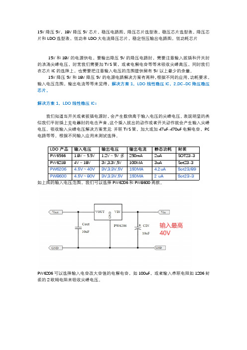
LDO产品输入电压输出电压输出电流静态功耗封装PW6566 1.8V~5.5V 1.2V~5V多250mA 2uA SOT23-3PW62184V~18V 3V,3.3V,5V 100MA 3uA Sot23-3PW6206 4.5V~40V3V,3.3V,5V150MA 4.2uA Sot23/89PW8600 4.5V~80V3V,3.3V,5V150MA 2 uA Sot23-3如上图的输入电压范围,我们可以选择PW6206和PW8600两款。
PW6206可以选择输入电容改大容值的电解电容,如100uF,或者输入串联电阻如1206封装的2欧姆电阻来吸收尖峰电压。
解决方案2,DC-DC降压电路芯片DC-DC降压产品输入电压输出电压输出电流频率封装PW2057 2.0V~6.0V 3.3V,1.8V,1.2V 0.7A 1.5MHz SOT23-5PW2058 2.0V~6.0V 1V~5V 0.8A 1.5MHz SOT23-5PW2051 2.5V~5.5V 1V~5V 1.5A 1.5MHz SOT23-5PW2052 2.5V~5.5V 1V~5V 2.0A 1.0 MHz SOT23-5PW2053 2.5V~5.5V 1V~5V 3.0A 1.0 MHz SOT23-5PW2162 4.5V~16V 1V~15V 2A 600KHZ SOT23-6PW2163 4.5V~16V 1V~15V 3A 600KHZ SOT23-6PW2205 4.5V~30V1V~25V5A500KHZ SOP8-EPPW2312 4.0V~30V1V~28V 1.2A 1.4 MHz SOT23-6PW2330 4.5V~30V1V~28V3A500KHz SOP8PW2431 4.5V~40V1V~30V3A340KHz SOP8-EPPW2558 4.5V~55V 1.25V~30V 0.8A 1.2 MHz SOT23-6PW2608 5.5V~60V 1.5-30V 0.8A 0.3-1Mhz SOP8-EPPW2815 4.5V~80V 1.5V~30V 1.5A 400KHZ SOP8-EPPW2906 12V~90V 1.25V~20V 0.6A 150KHZ SOP8-EPPW2902 8V~90V 5V~30V 2A 140KHZ SOP8-EPPW2153 8V~140V 5V~30V 4A 140KHZ SOP8降压芯片推荐输入电压最高到30V以上的芯片,图PW2312,PW2330,PW2431,PW2558等5V输出的测试图片没有拍,就发15V-18V降压输出12V的测试图片了。

15V降压5V18V降压5V的IC和LDO芯片的方案在设计数电路降压电源的过程中,需要选择适当的电压降低IC和LDO芯片来实现所需的降压功能。
以下是两种实现15V降压到5V和18V 降压到5V的方案。
方案一:15V降压到5V的IC和LDO芯片在15V降压到5V的设计中,我们可以选择LM7805稳压芯片作为LDO 芯片。
LM7805是一种三端稳压器,具有过热保护和过载保护功能,能够将高电压输入稳定到5V输出。
接下来,我们需要选择适当的降压IC来实现15V到5V的降压功能。
一种常用的降压IC是LM2596,它是一种开关稳压器,可以使用外部电感和电容实现高效的降压转换。
LM2596具有宽输入电压范围和可调输出电压功能,非常适合这种应用。
通过将15V输入连接到LM2596的输入引脚,将5V输出连接到LM7805的输入引脚,然后将LM7805的输出引脚连接到所需的负载,就可以实现15V降压到5V的功能。
方案二:18V降压到5V的IC和LDO芯片在18V降压到5V的设计中,我们同样可以选择LM7805作为LDO芯片来稳定输出电压。
与此同时,我们可以选择TPS5430作为降压IC来实现18V到5V的降压功能。
TPS5430是一款效率高的非同步降压DC-DC转换器,可以根据需要调整频率和占空比。
TPS5430具有宽输入电压范围和大输出电流能力,非常适合这种应用。
将18V输入连接到TPS5430的输入引脚,将5V输出连接到LM7805的输入引脚,然后将LM7805的输出引脚连接到所需的负载,就可以实现18V降压到5V的功能。
需要注意的是,在设计降压电源时,除了选择适当的芯片之外,还需要合理布局电路板、选择合适的电感和电容,并考虑散热和过载保护等因素,以确保电路的可靠性和稳定性。

6815芯片工作原理6815芯片的主要工作原理是基于一种称为VLIW(Very Long Instruction Word)的指令集体系结构。
VLIW是一种指令并行处理的技术,它允许多个指令同时执行,极大地提高了芯片的运算能力。
在6815芯片中,CPU核心是其中最重要的模块,它负责执行指令、控制数据流动和完成各种运算操作。
CPU核心包括多个处理单元,可以同时执行多个指令。
这些指令可以是不同类型的指令,例如算术指令、逻辑指令、分支指令等。
通过同时执行多个指令,CPU核心能够提高芯片的处理能力,实现更高效的运算。
浮点运算单元是另一个重要的功能模块,它负责执行浮点运算操作。
浮点运算是一种对于小数点的数进行操作的方法,它广泛应用于科学计算、图像处理和语音识别等领域。
浮点运算单元通过专门的硬件电路,能够高效地完成复杂的浮点运算操作,提高了芯片的浮点运算能力。
存储器是芯片的另一个关键模块,它用于存储数据和指令。
存储器是芯片的“记忆”部分,它可以分为内部存储器和外部存储器两部分。
内部存储器是芯片内部集成的存储器,速度快但容量有限;外部存储器是外接的存储器,容量大但速度较慢。
存储器在芯片的运算过程中发挥着至关重要的作用,它能够存储各种数据和指令,为CPU核心提供必要的数据支持。
总线接口是连接芯片与外部设备的接口,它负责数据的输入和输出。
总线接口可以连接到各种外部设备,例如显示器、键盘、存储器等。
通过总线接口,芯片能够与外部设备进行数据交互,实现更丰富的功能。
综上所述,6815芯片的工作原理是基于VLIW指令集体系结构,通过多个功能模块的协调工作,实现数据的输入、处理和输出。
CPU核心执行指令,浮点运算单元执行浮点运算操作,存储器存储数据和指令,总线接口连接外部设备,完成各种功能。
这种工作原理使得6815芯片能够实现高性能的数字信号处理功能,广泛应用于移动通信领域。

PL831036V, 1.5A Monolithic Step-Down Switching Regulator1 Features∙1.5A continuous output current capability∙ 4.5V to 36V wide operating input range with 33V input Over Voltage Protection∙ Integrated 36V, 250m Ω high side and 36V, 140m Ω low side power MOSFET switches ∙ Up to 97% efficiency∙ Internal Soft-Start limits the inrush current at turn-on ∙ Internal compensation to save external components ∙ Input Under-Voltage Lockout∙ Input over-voltage protection to protect device from working in high voltage and high current condition ∙ Output Over-Voltage Protection∙ Output short protection with both high side current limit and low side current limit to protect the device in hard short∙ Over-Temperature Protection∙ Pulse skip mode at light load to improve light load efficiency∙ Stable with Low ESR Ceramic Output Capacitors ∙ Fixed 150KHz Switching Frequency∙ Fewest external components and intensive internal protection features∙Available in SOP-8, ESOP8 and SOT23-6 Package2 Applications∙ USB car charger∙ Portable charging device∙General purpose DC-DC conversion3 DescriptionPL8310 is a monolithic 36V, 1.5A step-down switching regulator. PL8310 integrates a 36V 250m Ω high side and a 36V, 140m Ω low side MOSFETs to provide 1.5A continuous load current over a 4.5V to 36V wide operating input voltage with 33V input over voltage protection. Peak current mode control provides fast transient responses and cycle-by-cycle current limiting.PL8310 has configurable line drop compensation, configurable charging current limit. CC/CV mode control provides a smooth transition between constant current charging and constant voltage charging stages. Built-in soft-start prevents inrush current at power-up.4 Typical Application SchematicWork Mode 0: CS floating Work Mode 1: CS to GND with sensing resistorFig. 1 SchematicLEDFig. 2 Pin-out diagramFig. 3 Efficiency curveICQ:294 434 3362唐云:135****2646 QQ:29443533625 Pin Configuration and FunctionsLEDFBCSBSTPL8310 SOP-8 Package PL8310D ESOP-8 PackagePL8310C SOT23-6 PackageCSBSTENBSTPL8310E SOT23-6 Package PL8310F SOT23-6 PackagePL8310 Pin-Functions (SOP-8 Package)6 Device Marking InformationPL8310: Part NumberRAAYMD: RAA: LOT NO.; YMD: Package Date7 Specifications7.1 Absolute Maximum Ratings (Note1)7.2 Handling Ratings7.3 Recommended Operating Conditions (Note 2)PL8310 7.4 Thermal Information (Note 3)Notes:1) Exceeding these ratings may damage the device.2) The device function is not guaranteed outside of the recommended operating conditions.3) Measured on approximately 1” square of 1 oz copper.7.5 Electrical Characteristics (Typical at Vin = 12V, T J=25°C, unless otherwise noted.)Note:4) Guaranteed by design, not tested in production.8 Typical CharacteristicsVin = 12V, Vo = 5VCh1: SW Ch2:VOUT Ch3: VIN Ch4:IL Fig. 6 Startup waveform, Iout = 0AVin = 12V, Vo = 5VCh1: SW Ch2:VOUT Ch3: VIN Ch4:IL Fig. 7 Startup waveform, Iout = 1.5AVin = 24V, Vout = 5VCh1: SW Ch2:VOUT Ch3: VIN Ch4:IL Fig. 8 Startup waveform, Iout = 0AVin = 24V, Vout = 5VCh1: SW Ch2:VOUT Ch3: VIN Ch4:IL Fig. 9 Startup waveform, Iout = 1.5AVin = 12V, Vout = 5VCh1: SW Ch2:VOUT Ch3: VIN Ch4:IL Fig. 10 Steady state waveform, Iout = 0AVin = 12V, Vout = 5VCh1: SW Ch2:VOUT Ch3: VIN Ch4:IL Fig. 11 Steady state waveform, Iout = 1.5AVin = 24V, Vout = 5VCh1: SW Ch2:VOUT Ch3: VIN Ch4:IL Fig. 12 Steady state waveform, Iout = 0AVin = 24V, Vout = 5VCh1: SW Ch2:VOUT Ch3: VIN Ch4:IL Fig. 13 Steady state waveform, Iout = 1.5AVin = 12V, Vout = 5VCh1: SW Ch2:VOUT Ch3: VIN Ch4:IL Fig. 14 Shutdown waveform, Iout = 0AVin = 12V, Vout = 5VCh1: SW Ch2:VOUT Ch3: VIN Ch4:IL Fig. 15 Shutdown waveform, Iout = 1.5A9 Detailed Description9.1 OverviewPL8310 is an easy to use synchronous step-down DC-DC converter that operates from 4.5V to 36V supply voltage. It is capable of delivering up to 1.5A continuous load current with high efficiency and thermal performance in a very small solution size.PL8310 also integrates input over voltage and output over voltage protection. This feature helps customers to design a safe DC-DC converter easily.The switching frequency is fixed at 150 kHz switching frequency to minimize inductor size and improve EMI performance.9.2 Functional Block DiagramLEDFig.16 PL8310 Diagram9.3 Peak Current Mode ControlPL8310 employs a fixed 150 kHz frequency peak current mode control. The output voltage is sensed by an external feedback resistor string on FB pin and fed to an internal error amplifier. The output of error amplifier will compare with high side current sense signal by an internal PWM comparator. When the second signal is higher than the first one, the PWM comparator will generate a turn-off signal to turn off high side switch. The output voltage of error amplifier will increase or decrease proportionally with the output load current. PL8310 has a cycle-by-cycle peak current limit feature inside to help maintain load current in a safe region.9.4 Sleep Operation for Light Load EfficiencyPL8310 has an internal feature to help improving light load efficiency. When output current is low, PL8310 will go into sleep mode.9.5 Setting Output VoltageThe output voltage is set with a resistor divider from the output node to the FB pin. 1% resistance accuracy of this resistor divider is preferred. The output voltage value is set as equation 1 below (R1 is the upper resistor, R2 is the lower resistor).1(1)out refV ref is the internal reference voltage of PL8310, which is 0.9V.9.6 Setting Enable ThresholdWhen the voltage at EN pin exceeds the threshold, PL8310 begins to work. When keeping EN low (below threshold), PL8310 stops working. The quiescent current of PL8310 is very low to maintain a good shut down operation for system. PL8310 has an internal pull up resistor to make sure IC work when EN pin is float. If an application requires to control EN pin, use open drain or open collector output logic circuit to interface with it.When system needs a higher VIN UVLO threshold, the EN pin can be configured as shown in Figure 17 below.Fig.17 Adjustable VIN Under voltage Lockout9.7 Slope CompensationIn order to avoid sub-harmonic oscillation at high duty cycle, PL8310 adds a slope compensation ramp to the sensed signal of current flowing through high side switch.9.8 Error AmplifierThe error amplifier compares the FB voltage against the internal reference (V ref) and outputs a current proportional to the difference between these two signals. This output current charges or discharges the internal compensation network to generate the error amplifier output voltage, which is used to control the power MOSFET current. The optimized internal compensation network minimizes the external component counts and simplifies the control-loop design.9.9 Bootstrap Voltage provided by internal LDOPL8310 has an internal LDO to provide energy consumed by high side switch. At BST pin, PL8310 needs a small ceramic capacitor like 100nF between BST and SW pin to provide gate-drive voltage for high side switch. The bootstrap capacitor is charged when high side is off. In Continuous-Current-Mode, the bootstrap capacitor will be charged when low side is on. The bootstrap capacitor voltage will be maintained at about 5.3V. When IC works under sleep mode, what value the bootstrap capacitor is charged depends on the difference of Vin and output voltage. However, when the voltage on the bootstrap capacitor is below bootstrap voltage refresh threshold, PL8310 will force low side on to charge bootstrap capacitor. Connecting an external diode from the output of regulator to the BST pin will also work and increase the efficiency of the regulator when output is high enough.9.10 High Side Over-Current ProtectionIn PL8310, high-side MOSFET current is sensed. This sensed signal will compare the lower voltage between COMP pin voltage and over current threshold. High-side MOSFET will be turned off when the sensed current reaches the lower voltage. In normal operation, COMP pin voltage will be lower. If the over current threshold is lower, PL8310 enters over current protection mode.9.11 Thermal ShutdownThe internal thermal-shutdown circuitry forces the device to stop switching if the junction temperature exceeds 155°C typically. When the junction temperature drops below 140°C, IC will start to work again.9.12 Setting current limitA current sensing resistor R3 can be used to adjust current limit. The following equation can be used to calculate the needed resistor value.Ω9.13 Line drop compensationWhen USB charging cable line is long and resistance is high, there will be some significant voltage drop on the cable. Portable device will see much lower input voltage. If the voltage across the load input terminals is too low, it will affect the charge time for the load. It is recommended to adjust the output voltage of charger to compensate this voltage drop. PL8310 has an configurable line drop compensation feature. The line drop compensation value can be programmed by the top feedback resistor R1 in Fig 1. The line compensation voltage can be roughly calculated as following:ΔVout=R cs*I out*15*R1/200kΩR cs is the sum of current sensing resistor on CS pin, all of the parasitic resistance on PCB board and GND pin. I out is output load current going through R cs. R1 is the top feedback resistor.10 Application and Implementation10.1 Inductor selectionAn inductor is required to supply constant current to the load while being driven by the switched input voltage. A larger value inductor will result in less current ripple and lower output voltage ripple. However, the larger value inductor will have larger physical size, higher DC resistance, and/or lower saturation current. A good rule to calculate the inductance is to allow the peak-to-peak ripple current in the inductor to be approximately 25% of the maximum load current. At the same time, it is needed to make sure that the peak inductor current is below the inductor saturation current.The inductance value can be calculated by:1-(2)f sWhere V OUT is the output voltage, V IN is the input voltage, f S is the switching frequency, and Δ L is the peak-to-peak inductor ripple current.Choose an inductor that will not saturate under the maximum peak current. The peak inductor current can be calculated by:1-(3)load fsWhere I load is the load current.The choice of inductor material mainly depends on the price vs. size requirements and EMI constraints.10.2 Optional Schottky DiodeDuring the transition between the high-side switch and low-side switch, the body diode of the low-side power MOSFET conducts the inductor current. The forward voltage of this body diode is high. An optional Schottky diode may be paralleled with low side MOSFET to improve overall efficiency. Table 2 lists example Schottky diodes and their Manufacturers.10.3 Input capacitors selectionThe input current to the step-down converter is discontinuous, therefore a capacitor is required to supply the AC current to the converter. It is recommend to use low ESR capacitors to optimize the performance. Ceramic capacitor is preferred, but tantalum or low-ESR electrolytic capacitors may also meet the requirements. It is better to choose X5R or X7R dielectrics when using ceramic capacitors.Since the input capacitor (C IN) absorbs the input switching current, a good ripple current rating is required for the capacitor. The RMS current in the input capacitor can be estimated by:1-(4)loadThe worst-case condition occurs at V IN = 2×V OUT, where:load(5) For simplification, choose the input capacitor whose RMS current rating is greater than half of the maximum load current.When electrolytic or tantalum capacitors are used, a small, high quality ceramic capacitor, i.e. 0.1µF, should be placed as close to the IC as possible. When ceramic capacitors are used, make sure that they have enough capacitance to maintain voltage ripple at input. The input voltage ripple caused by capacitance can be estimated by:load1-(6)f sC IN is the input capacitance.10.4 Output capacitors selectionThe output capacitor (C OUT) is required to maintain the DC output voltage. Ceramic, tantalum, or low ESR electrolytic capacitors are recommended.Low ESR capacitors are preferred to keep the output voltage ripple low. The output voltage ripple can be estimated by:f s 1-1f s(7)Where L is the inductor value, R ESR is the equivalent series resistance (ESR) value of the output capacitor and C OUT is the output capacitance value. In the case of ceramic capacitors, the impedance at the switching frequency is dominated by the capacitance. The output voltage ripple is mainly determined by the capacitance. For simplification, the output voltage ripple can be estimated by:f s1-(8)In the case of tantalum or electrolytic capacitors, the ESR dominates the impedance at the switching frequency. For simplification, the output ripple can be approximated to:f s1-(9)The characteristics of the output capacitor also affect the stability of the regulator. PL6320is optimized for a wide range of capacitance and ESR values..11 PCB Layout11.1 GuidelinePCB layout is a critical portion of good power supply design. The following guidelines will help users design a PCB with the best power conversion efficiency, thermal performance, and minimized EMI.1. The feedback network, resistor R1 and R2, should be kept close to FB pin. V out sensing path should stay awayfrom noisy nodes, such as SW and BST signals. The ground of R2 should be connected directly to GND pin by a single point. An optional 47pF capacitor C6 may be needed to improve the noise immunity for a poor placed PCB.2. The input bypass capacitor C1 and C2 must be placed as close as possible to V IN pin and GND pin. Groundingfor both the input and output capacitors should consist of localized top side planes. Make the GND plane as big as possible for best thermal performance.3. Place current sense resister R3 as close as possible to the chip and stay away from noisy nodes such as SW,BST.4. Input capacitor, output capacitor, inductor and PL8310 should be placed evenly on the PCB board for the bestthermal performance. Separate PL8310 from inductor as much as possible since they are the hottest components on the PCB.5. R6, C4 may be needed to improve EMI in some design. The parameters for these components could beR6=4.7Ohm, C4=2.2nF. Connect R6 to SW and C4 to gnd. Place these two components close to SW pin and GND pin for the best EMI performance.6. An external schottky diode may be needed to improve the current loading capability. Place the diode close to SWand GND pin as close as possible.11.2 ExampleWork Mode 0: CS floating Fig.18 SchematicWork Mode 0: CS floating Fig.19 PCB LayoutC3Work Mode 1: CS to GND with sensing resistor or short to GND directlyFig.20 SchematicC2, C6, C9 are optional, R6, C4 are used to improve EMI onlyWork Mode 1: CS to GND with sensing resistor or short to GND directlyFig.21 PCB Layout12 Packaging Information13 Taping OrientationIMPORTANT NOTICESiipower T ch. assumes no responsibility for any error which may appear in this document. Powlicon Inc. reserves the right to change devices or specifications detailed herein at any time without notice. Siipowe Tch.does not assume any liability arising out of the application or use of any product described herein; neither it does it convey any license under its patent rights, nor the rights of others. Siipower Tch. products are not authorized for use as critical components in life support devices or systems without written approval letter from the Chief Executive Officer of Siipower Tch.. The user of products in such applications shall assume all risks of such use and will agree to not hold against Powlicon Inc. for all damages.。

1.5MHz的800mA同步降压稳压器-TD6810
TD6810是一个高效率单片同步降压型稳压器采用恒定频率,电流模式架构。
该装置是在版本可调及固定输出电压为1.5V和1.8V。
在操作过程中电源电流只有20mA和下降到≤ 1毫安关机。
2.5V至5.5V 的输入电压范围使其非常适用于单节锂离子电池供电的应用TD6810。
100%占空比提供低漏失操作,延长电池寿命增加在便携式systems.Automatic的突发模式操作在轻负载时的效率,进一步延长电池life.Switching的频率被内部设置为1.5MHz,允许使用小型表面贴装电感器和电容器内部同步开关提高了效率,并省去了对外部肖特基二极管。
低输出电压很容易支持与0.6V反馈参考电压。
TD6810是低调(1毫米)TSOT 23-5 封装。
特点
*高效率:高达96%
*在轻负载时的高效率
*非常低的静态电流:只有20 ü A在操作
* 8 00毫安输出电流
* 2.5V至5.5V输入电压范围
* 1.5MHz恒定频率操作
*无需肖特基二极管
*低压差操作:100%占空比
* 0.6V基准允许低输出电压
*关机模式绘制≤ 1 ü的电源电流
*出色的线路和负载瞬态响应的电流模式操作
*过热保护
*低调(1mm)TSOT 23-5 包装
应用
*蜂窝电话
*个人信息设备
*无线和DSL调制解调器
*数码相机
* MP3播放器*便携式仪器。
6815芯片工作原理6815芯片是一种常用的集成电路芯片,主要应用于各种电子设备中。
本文将详细介绍6815芯片的工作原理。
一、概述6815芯片是一种高性能、低功耗的集成电路芯片,其工作原理是通过不同的电路模块相互配合来完成各种功能。
该芯片由处理器核心、存储器、输入输出接口、时钟模块以及各种外设模块等组成。
二、处理器核心6815芯片的处理器核心采用先进的架构设计,具有较高的计算速度和处理能力。
它能够执行各种指令,控制芯片的运行,并与其他模块进行通信和数据交换。
处理器核心是6815芯片的"大脑",起着决策和控制的作用。
三、存储器6815芯片内置了多种存储器,包括闪存、随机访问存储器(RAM)等。
闪存用于存储程序代码和数据,RAM用于临时存储数据。
存储器模块能够快速读写数据,提高芯片的运行效率。
四、输入输出接口6815芯片的输入输出接口模块用于与外部设备进行数据交换。
它支持多种接口标准,如串行接口、并行接口等。
通过这些接口,芯片可以连接各种外设设备,如显示器、键盘、鼠标等,实现数据输入输出功能。
五、时钟模块6815芯片内置了时钟模块,用于提供精确的时钟信号。
时钟信号是芯片运行的基准,能够同步各个模块的工作,确保芯片的正常运行。
时钟模块具有较高的稳定性和精度,能够满足各种应用场景的需求。
六、外设模块6815芯片还内置了各种外设模块,如通信模块、音频模块、图形处理模块等。
这些模块能够实现与外部设备的数据交换和处理,为用户提供更加丰富的功能和体验。
七、工作原理6815芯片的工作原理是通过处理器核心控制各个模块的协同工作来实现功能。
首先,处理器核心根据程序指令从存储器中读取相应的数据和指令,然后通过输入输出接口与外部设备进行数据交换。
同时,时钟模块提供稳定的时钟信号,同步各个模块的工作。
外设模块根据处理器核心的指令进行相应的数据处理和功能实现。
八、应用领域6815芯片广泛应用于各种电子设备中,如智能手机、平板电脑、电视机、路由器等。
6815芯片工作原理6815芯片是一种集成电路芯片,具有多种功能和应用。
本文将介绍6815芯片的工作原理。
我们来了解一下6815芯片的基本结构。
6815芯片由多个功能模块组成,包括处理器、存储器、输入输出接口等。
这些模块相互连接,协同工作,实现各种功能。
6815芯片的工作原理涉及到处理器的运算和控制过程。
处理器是芯片的核心部分,负责执行各种指令,进行数据处理和控制操作。
处理器内部有多个寄存器,用于存储和传输数据。
当处理器接收到指令时,会按照指令的要求进行相应的数据处理并输出结果。
6815芯片的存储器模块用于存储数据和程序。
存储器分为内部存储器和外部存储器两部分。
内部存储器速度快,容量小,用于存储临时数据和程序代码;外部存储器容量大,速度相对较慢,用于长期存储数据和程序。
输入输出接口模块是6815芯片与外部设备进行数据交换的通道。
通过输入输出接口,芯片可以与键盘、鼠标、显示器、打印机等外部设备进行数据的输入和输出。
输入输出接口模块会将外部设备传输的数据转换为芯片内部可以处理的格式,并将芯片内部的数据转换为外部设备可以识别的格式进行输出。
在6815芯片的工作过程中,还涉及到时钟和控制信号的生成和传输。
时钟信号用于同步芯片内部各个模块的工作,保证各个模块可以按照统一的节拍进行工作。
控制信号用于控制各个模块的工作状态和操作。
总结一下,6815芯片的工作原理可以概括为:处理器接收指令和数据,按照指令要求进行数据处理并输出结果;存储器用于存储数据和程序;输入输出接口用于与外部设备进行数据交换;时钟和控制信号用于同步和控制各个模块的工作。
6815芯片具有广泛的应用领域,例如智能手机、平板电脑、电视机、汽车电子等。
它的工作原理的理解对于我们理解和应用这些设备都具有重要意义。
通过了解6815芯片的工作原理,我们可以更好地利用和开发它的功能,实现更多的应用和创新。
15V降压12V,18V降压12V电源芯片,降压芯片,电路图,大电流降压芯片,极高效率降压IC,电源芯片降压选型表15V降压12V和18V降压12V的电源芯片,适合1-5A大电流应用等,根据不同的输入电压来选择,15V和18V降压12V解决方案比较推荐:DC-DC降压电路了。
DC-DC降压电路:输入电压输出电压输出电流频率封装DC-DC降压产品PW2058 2.0V~6.0V 1V~5V 0.8A 1.5MHz SOT23-5PW2051 2.5V~5.5V 1V~5V 1.5A 1.5MHz SOT23-5PW2052 2.5V~5.5V 1V~5V 2.0A 1.0 MHz SOT23-5PW2053 2.5V~5.5V 1V~5V 3.0A 1.0 MHz SOT23-5PW2162 4.5V~16V 1V~15V 2A 600KHZ SOT23-6PW2163 4.5V~16V 1V~15V 3A 600KHZ SOT23-6PW2205 4.5V~30V1V~15V5A500KHZ SOP8-EPPW2312 4.0V~30V1V~28V 1.2A 1.4 MHz SOT23-6PW2330 4.5V~30V1V~28V3A500KHz SOP8PW2431 4.5V~40V1V~30V3A340KHz SOP8-EPPW2558 4.5V~55V 1.25V~30V0.8A 1.2 MHz SOT23-6PW2608 5.5V~60V 1.5-30V 0.8A 0.3-1Mhz SOP8-EPPW2815 4.5V~80V 1.5V~30V 1.5A 400KHZ SOP8-EPPW2906 12V~90V 1.25V~20V 0.6A 150KHZ SOP8-EPPW2902 8V~90V 5V~30V 2A 140KHZ SOP8-EPPW2153 8V~140V 5V~30V 4A 140KHZ SOP8。
DC-DC 降压转换器产品概述PW2051 是一款由基准电压源、振荡电路、比较器、 PWM/PFM 控制电路等构成的 CMOS 降压型 DC/DC 调整器。
利用 PWM/PFM 自动切换控制电路达到可调占空比,具有全输入电压范围内的低纹波、高效率和大输出电流等特点。
PW2051 内置功率 MOSFET, 集成了过压、过流、过热、 短路等诸多保护电路,在超过控制值时会自动断开,以保护芯片。
本产品结合了微型封装和低消耗电流等特点,最适合在移动设备的电源内部使用。
PW2051采用SOT23-5L 封装配合较少的外围原件使其非常适用于便携式产品.产品特点● 最大效率可达 95% ● 最大输出电流 1.5A ● 超低静态电流 40μA ● 甚小输出纹波 <±0.4%● 低压操作 可达 100%占空比● PWM/PFM 自动切换 占空比自动可调以保持全负载范围内的高效率、低纹波 ●短路保护应用范围● 数码相机、电子记事本、 PDA 等移动设备电源 ● 照相机、视频设备、通信设备的稳压电源 ● 微机电源 ●机顶盒典型应用电路C1为可选电容代理深圳夸克微科技引脚配置/说明引脚号 符号 引脚说明 1 CE 芯片使能端,高有效 2 GND 地3 LX 内部功率开关输出端口4 VIN 电源输入端 5FB输出电压反馈端绝对最大额定值项目 符号 绝对最大额定值 单位 输入电压 VIN -0.3~6.5V 输出电压 VFB -0.3~6.5 V VLX -0.3~VIN + 0.3 V CE 端电压 VCE -0.3~VIN + 0.3 V LX 端电流 ILX ±2 A 容许功耗 Pd 250 mW 工作环境温度 Topr -40~+85 ℃ 保存温度Tstg-55~+125℃CE GND LX FBSOT-23-5L (TOP VIEW)VIN12345PCB 布局为了使噪音最低和操作性能最佳, PCB 布局时以下几点建议可作为参考: 1、 VIN、 LX 、 GND 组成的功率通路,尽量采用短而宽的布线,避免过孔。
General DescriptionThe TD6811 is a high efficiency monolithic synchronousbuck regulator using a constant frequency, current mode architecture. The device is available in an adjustable version and fixed output voltages of 1.5V and 1.8V.Supply current during operation is only 20mA and drops to ≤1mA in shutdown. The 2.5V to 5.5V input voltage range makes the TD6811 ideally suited for single Li-Ion battery-powered applications. 100% duty cycle provides low dropout operation, extending battery life in portable systems.Automatic Burst Mode operation increases efficiency at light loads, further extending battery life. Switching frequency is internally set at 1.5MHz, allowing the use of small surface mount inductors and capacitors.The internal synchronous switch increases efficiency and eliminates the need for an external Schottky diode. Low output voltages are easily supported with the 0.6Vfeedback reference voltage. The TD6811 is available in TSOT23-5 package.Featuresz High Efficiency: Up to 96% z High Efficiency at light loadsz Very Low Quiescent Current: Only 20uA DuringOperationz 1.2A Output Currentz 2.5V to 5.5V Input Voltage Range z 1.5MHz Constant Frequency Operation z No Schottky Diode Requiredz Low Dropout Operation: 100% Duty Cycle z 0.6V Reference Allows Low Output Voltages z Shutdown Mode Draws ≤1uA Supply Currentz Current Mode Operation for Excellent Line and LoadTransient Response z Overtemperature Protected z TSOT23-5 Package is AvailableApplicationsz Cellular Telephonesz Personal Information Appliances z Wireless and DSL Modems z Digital Still Cameras z MP3 Players z Portable InstrumentsPackage TypesFigure1. Package Types of TD6811TSOT235Pin AssignmentsTSOT23‐5Pin Name Description1 RUNRun Control Input. Forcing this pin above 1.5V enables the part. Forcing this pin below 0.3V shuts down the device. In shutdown, all functions are disabled drawing <1μA supply current. Do not leave RUN floating.2 GND Ground Pin.3 SW Switch Node Connection toInductor. This pin connects to the drains of the internal main and synchronous power MOSFET switches.4 VIN Main Supply Pin. Must be closelydecoupled to GND, Pin 2, with a2.2μF or greater ceramic capacitor.5 VFB Feedback Pin. Receives thefeedback voltage from an external resistive divider across the output. 5 VOUTOutput Voltage Feedback Pin. An internal resistive divider divides the output voltage down for comparison to the internal reference voltage.Ordering InformationTD6811 □ □Circuit Type Output Versions Blank :Adj 12:1.2V Package 15:1.5V T:TSOT23-5 18:1.8VFunctional Block DiagramFigure2:Functional Block Diagram of TD6811Type Application CircuitFigure 3. Type Application Circuit of TD6811Absolute Maximum RatingsNote1: Stresses greater than those listed under Maximum Ratings may cause permanent damage to the device. This is a stress rating only and functional operationof the device at these or any other conditions above those indicated in the operation is not implied. Exposure to absolute maximum rating conditions for extendedperiods may affect reliability.Parameter ValueUnit Input Supply Voltage -0.3 ~6 VRUN, VFB Voltages -0.3 ~ VIN VSW Voltage -0.3V ~(VIN+0.3) VP-Channel Switch Source Current (DC) 1500 mAN-Channel Switch Sink Current (DC) 1500 mAPeak SW Sink and Source Current 1.8 AOperating Temperature Range -40~+85 ºCJunction Temperature 125 ºCLead Temperature (Soldering, 10 sec) 300 ºCStorage Temperature Range -65~150 ºCElectrical CharacteristicsUnless otherwise specified, VIN= 3.6V TA=25 ºC.Symbol Parameter Conditions Min.Typ.Max.UnitIVFB FeedbackCurrent 30 nAVFB Regulated FeedbackVoltageTA = 25°C 0.5880 0.6000 0.6120V0°C TA ≤ 85°C 0.5865 0.6000 0.6135–40°C ≤ TA ≤ 85°C 0.5850 0.6000 0.6150VFB Reference Voltage LineRegulationVIN = 2.5V to 5.5V 0.04 0.4 %/ VVOUT Regulated OutputVoltageTD6811-1.5, IOUT = 100mA 1.455 1.500 1.545 VTD6811-1.8, IOUT = 100mA 1.746 1.800 1.854VOUT Output Voltage LineRegulationVIN = 2.5V to 5.5V 0.04 0.4 %/ VElectrical Characteristics(Cont.)Unless otherwise specified, VIN= 3.6V TA=25 ºC.Symbol Parameter Conditions Min.Typ.Max.UnitIPK Peak Inductor Current VIN = 3V, VFB = 0.5V orVOUT = 90%, Duty Cycle <35%1.55 1.6 1.7 AVLOADREG Output Voltage LoadRegulation0.5%VIN Input Voltage Range 2.5 5.5 VIS Input DC Bias CurrentActive ModeVFB = 0.5V or VOUT =90%, ILOAD = 0A300400uA Sleep ModeVFB = 0.62V or VOUT =103%, ILOAD = 0A2035uA Shutdown VRUN = 0V, VIN = 4.2V 0.1 1 uAfOSCOscillator Frequency VFB = 0.6V or VOUT =100%1 1.52 MHz VFB = 0V or VOUT = 0V 400 KHzRPFET RDS(ON) of P-ChannelFETISW = 100mA 0.30 0.40 ΩRNFET RDS(ON) of N-ChannelFETISW = -100mA 0.30 0.40 ΩILSW SWLeakage VRUN = 0V, VSW = 0V or5V, VIN = 5V0.011 uAVRUN RUNThreshold 0.31 1.5V IRUN RUN Leakage Current 0.01 1 uATypical Operating CharacteristicsOscillator Frequency Reference VoltageOscillator Frequency vs Supply VoltageRDS(ON) vs TemperatureTypical Operating Characteristics(Cont.)Efficiency vs Output Current RDS(ON) vs Input VoltageEfficiency vs Output CurrentEfficiency vs Output CurrentTypical Operating Characteristics(Cont.)Output Voltage vs Output Current Efficiency vs Output CurrentEfficiency vs Input Voltage Dynamic Supply Current vs Supply VoltageTypical Operating CharacteristicsN-FET Leakage vs Temperature P-FET Leakage vs TemperatureFunction DescriptionMain Control LoopThe TD6811 uses a constant frequency, current mode step-down architecture. Both the main (P-channel MOSFET) and synchronous (N-channel MOSFET) switches are internal. During normal operation, the internal top power MOSFET is turned on each cycle when the oscillator sets the RS latch, and turned off when the current comparator, ICOMP, resets the RS latch. The peak inductor current at which ICOMP resets the RS latch, is controlled bythe output of error amplifier EA. When the load current increases, it causes a slight decrease in the feedback voltage, FB, relative to the 0.6V reference, which in turn, causes the EA amplifier’s output voltage to increase until the average inductor current matches the new load current. While the top MOSFET is off, the bottom MOSFET is turned on until either the inductor current starts to reverse, as indicated by the current reversal comparator IRCMP, or the beginning of the next clock cycle.Burst Mode OperationThe TD6811 is capable of Burst Mode operation in which the internal power MOSFETs operate intermittently based on load demand.In Burst Mode operation, the peak current of the inductor is set to approximately 200mA regardless of the output load. Each burst event can last from a few cycles at light loads to almost continuously cycling with short sleep intervals at moderate loads. In between these burst events, the power MOSFETs and any unneeded circuitry are turned off, reducing the quiescent current to 20mA. In this sleep state, the load current is being supplied solely from the output capacitor. As the output voltage droops, the EA amplifier’s output rises above the sleep threshold signaling the BURST comparator to trip and turn the top MOSFET on. This process repeats at a rate that is dependent on the load demand.ShortCircuit ProtectionWhen the output is shorted to ground, the frequency of the oscillator is reduced to about 400kHz, 1/4 the nominal frequency. This frequency foldback ensures that the inductor current has more time to decay, thereby preventing runaway. The oscillator’s frequency will progressively increase to 1.5MHz when VFB or VOUT rises above 0V.Dropout OperationAs the input supply voltage decreases to a value approaching the output voltage, the duty cycle increases toward the maximum on-time. Further reduction of the supply voltage forces the main switch to remain on for more than one cycle until it reaches 100% duty cycle. The output voltage will then be determined by the input voltage minus the voltage drop across the P-channel MOSFET and the inductor.An important detail to remember is that at low input supply voltages, the RDS(ON) of the P-channel switch increases (see Typical Performance Characteristics). Therefore, the user should calculate the power dissipation when the TD6811 is used at 100% duty cycle with low input voltage (See Thermal Considerations in the Applications Informationsection).Function Description(Cont.)Low Supply OperationThe TD6811 will operate with input supply voltages as low as 2.5V, but the maximum allowable output current isreduced at this low voltage. Figure 2 shows the reduction in the maximum output current as a function of input voltage for various output voltages.Slope Compensation and Inductor Peak CurrentSlope compensation provides stability in constant frequency architectures by preventing subharmonic oscillations at high duty cycles. It is accomplishedinternally by adding a compensating ramp to the inductor current signal at duty cycles in excess of 40%. Normally,this results in a reduction of maximum inductor peak current for duty cycles >40%. However, the TD6811 uses a patent-pending scheme that counteracts this compensating ramp, which allows the maximum inductor peak current to remain unaffected throughout all duty cycles.Maximum Output Current vs Input VoltagThe basic TD6811 application circuit is shown in Figure 3. External component selection is driven by the load requirement and begins with the selection of L followed by CIN and COUT.Inductor Selection For most applications, the value of the inductor will fall inthe range of 1mH to 4.7mH. Its value is chosen based onthe desired ripple current. Large value inductors lowerripple current and small value inductors result in higher ripple currents. Higher VIN or VOUT also increases theripple current as shown in equation 1. A reasonable starting point for setting ripple current is DIL = 480mA(40% of 1200mA).The DC current rating of the inductor should be at least equal to the maximum load current plus half the ripple current to prevent core saturation. Thus, a 1320mA rated inductor should be enough for most applications (1200mA + 120mA). For better efficiency, choose a low DC-resistanceinductor.The inductor value also has an effect on Burst Mode operation. The transition to low current operation begins when the inductor current peaks fall to approximately 200mA. Lower inductor values (higher DIL) will cause this to occur at lower load currents, which can cause a dip in efficiency in the upper range of low current operation. In Burst Mode operation, lower inductance values will cause the burst frequency to increase.Function Description(Cont.)Inductor Core SelectionDifferent core materials and shapes will change thesize/current and price/current relationship of an inductor. Toroid or shielded pot cores in ferrite or permalloy materials are small and don’t radiate much energy, but generally cost more than powdered iron core inductors with similar electrical characteristics. The choice of which style inductor to use often depends more on the price vs size requirements and any radiated field/EMI requirements than on what the TD6811 requires to operate. Table 1 shows some typical surface mount inductors that work well in TD6811 applications.Table 1. Representative Surface Mount Inductors CIN and COUT SelectionIn continuous mode, the source current of the top MOSFET is a square wave of duty cycle VOUT/VIN. To prevent large voltage transients, a low ESR input capacitor sized for the maximum RMS current must be used. The maximum RMS capacitor current is given by:This formula has a maximum at VIN = 2VOUT, where IRMS = IOUT/2. This simple worst-case condition is commonly used for design because even significant deviations do not offer much relief. Note that the capacitor manufacturer’s ripple current ratings are often based on 2000 hours of life. This makes it advisable to further derate the capacitor, or choose a capacitor rated at a higher temperature than required. Always consult the manufacturer if there is any question.The selection of COUT is driven by the required effective series resistance (ESR). Typically, once the ESR requirement for COUT has been met, the RMS currentrating generally far exceeds the IRIPPLE(P-P) requirement. The output ripple DVOUT is determined by:where f = operating frequency, COUT = outputcapacitanceand DIL = ripple current in the inductor. For afixed output voltage, the output ripple is highest at maximum input voltage since DIL increases with inputvoltage.Aluminum electrolytic and dry tantalum capacitors are both available in surface mount configurations. In the case of tantalum, it is critical that the capacitors are surge tested for use in switching power supplies. An excellent choice is the AVX TPS series of surface mount tantalum. These are specially constructed and tested for low ESR so they give the lowest ESR for a given volume. Other capacitor types include Sanyo POSCAP, KemetT510 and T495 series, and Sprague 593D and 595D series. Consult the manufacturer for other specific recommendations.Function Description(Cont.)Using Ceramic Input and Output CapacitorsHigher values, lower cost ceramic capacitors are now becoming available in smaller case sizes. Their high ripple current, high voltage rating and low ESR make them ideal for switching regulator applications. Because the TD6811’s control loop does not depend on the output capacitor’s ESR for stable operation, ceramic capacitors can be used freely to achieve very low output ripple and small circuit size.However, care must be taken when ceramic capacitors are used at the input and the output. When a ceramic capacitor is used at the input and the power is supplied by a wall adapter through long wires, a load step at the output can induce ringing at the input, VIN. At best, this ringing can couple to the output and be mistaken as loop instability. At worst, a sudden inrush of current through the long wires can potentially cause a voltage spike at VIN, large enough to damage the part.When choosing the input and output ceramic capacitors, choose the X5R or X7R dielectric formulations. These dielectrics have the best temperature and voltage characteristics of all the ceramics for a given value and size.Output Voltage ProgrammingIn the adjustable version, the output voltage is set by a resistive divider according to the following formula:The external resistive divider is connected to the output, allowing remote voltage sensing as shown in Figure4.Figure 4:Setting the output VoltageVout R1 R21.2V 150K 150K1.5V 160K 240K1.8V 150K 300K2.5V 150K 470K3.3V 150K 680KTable 2. Vout VS. R1, R2, Cf Select Table Efficiency ConsiderationsThe efficiency of a switching regulator is equal to the output power divided by the input power times 100%. It is often useful to analyze individual losses to determine what is limiting the efficiency and which change would produce the most improvement. Efficiency can be expressed as:Efficiency = 100% – (L1 + L2 + L3 + ...)where L1, L2, etc. are the individual losses as a percentage of input power.Although all dissipative elements in the circuit produce losses, two main sources usually account for most of the losses in TD6811 circuits: VIN quiescent current and I2R losses. The VIN quiescent current loss dominates the efficiency loss at very low load currents whereas the I2R loss dominates the efficiency loss at medium to high load currents. In a typical efficiency plot, the efficiency curve at very low load currents can be misleading since the actual power lost is of no consequence as illustrated in Figure 5.Function Description(Cont.)Figure 4:Power Lost VS Load Current1. The VIN quiescent current is due to two components: the DC bias current as given in the electrical characteristics and the internal main switch and synchronous switch gate charge currents. The gate charge current results from switching the gate capacitance of the internal power MOSFET switches. Each time the gate is switched from high to low to high again, a packet of charge, dQ, moves from VIN to ground. The resulting dQ/dt is the current out of VIN that is typically larger thanthe DC bias current. In continuous mode, IGATECHG=f(QT + QB) where QT and QB are the gate charges of the internal top and bottom switches. Both the DC bias and gate charge losses are proportional to VIN and thustheir effects will be more pronounced at higher supply voltages.2. I2R losses are calculated from the resistances of the internal switches, RSW, and external inductor RL. In continuous mode, the average output current flowing through inductor L is “chopped” between the main switch and the synchronous switch. Thus, the series resistance looking into the SW pin is a function of both top and bottom MOSFET RDS(ON) and the duty cycle (DC) as follows: RSW = (RDS(ON)TOP)(DC) + (RDS(ON)BOT)(1 – DC) The RDS(ON) for both the top and bottom MOSFETs can be obtained from the Typical Performance Charateristics curves. Thus, to obtain I2R losses, simply add RSW to RL and multiply the result by the square of the average output current. Other losses including CIN and COUT ESR dissipative losses and inductor core losses generally account for less than 2% total additional loss.Thermal ConsiderationsIn most applications the TD6811 does not dissipate much heat due to its high efficiency. But, in applications where the TD6811 is running at high ambient temperature with low supply voltage and high duty cycles, such as in dropout, the heat dissipated may exceed the maximum junction temperature of the part. If the junction temperature reaches approximately 150°C, both power switches will be turned off and the SW node will become high impedance.To avoid the TD6811 from exceeding the maximum junction temperature, the user will need to do some thermal analysis. The goal of the thermal analysis is to determine whether the power dissipated exceeds the maximum junction temperature of the part. The temperature rise is given by:TR = (PD)(qJA)where PD is the power dissipated by the regulator and qJA is the thermal resistance from the junction of the die to the ambient temperature.The junction temperature, TJ, is given by:TJ = TA + TRwhere TA is the ambient temperature.As an example, consider the TD6811 in dropout at an input voltage of 2.7V, a load current of 800mA and an ambient temperature of 70°C. From the typical performance graph of switch resistance, the RDS(ON) of the P-channel switch at 70°C is approximately 0.52W.Function Description(Cont.)Therefore,power dissipated by the part is:PD = ILOAD 2 • RDS(ON) = 187.2mWFor the SOT-23 package, the qJA is 250°C/ W. Thus, the junction temperature of the regulator is:TJ = 70°C + (0.1872)(250) = 116.8°Cwhich is below the maximum junction temperature of 125°C.Note that at higher supply voltages, the junction temperature is lower due to reduced switch resistance (RDS(ON)).Checking Transient ResponseThe regulator loop response can be checked by lookingat the load transient response. Switching regulators take several cycles to respond to a step in load current. When a load step occurs, VOUT immediately shifts by an amount equal to (ΔILOAD • ESR), where ESR is the effective series resistance of COUT. ΔILOAD also begins to charge or discharge COUT, which generates a feedback error signal. The regulator loop then acts to return VOUT to its steadystate value. During this recovery time VOUT can be monitored for overshoot or ringing that would indicate a stability problem. For a detailed explanation of switching control loop theory.A second, more severe transient is caused by switchingin loads with large (>1μF) supply bypass capacitors. The discharged bypass capacitors are effectively put in parallel with COUT, causing a rapid drop in VOUT. No regulator can deliver enough current to prevent this problem if the load switch resistance is low and it isdriven quickly. The only solution is to limit the rise time of the switch drive so that the load rise time is limited to approximately (25 • CLOAD).Thus, a 10μF capacitor charging to 3.3V would require a 250μs rise time, limiting the charging current to about 130mA.Package InformationTSOT235 Package Outline DimensionsDesign Notes。