真空溅镀p
- 格式:ppt
- 大小:686.00 KB
- 文档页数:50
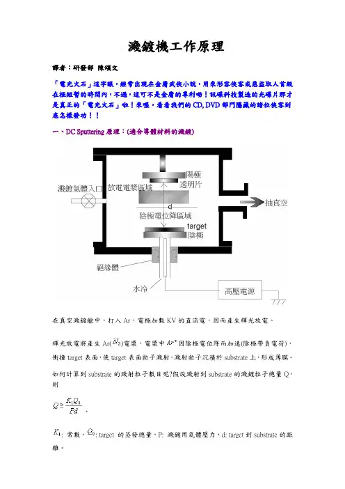
濺鍍機工作原理譯者:研發部陳頌文「電光火石」這字眼,經常出現在金庸武俠小說,用來形容俠客或惡盜取人首級在極短暫的時間內,不過,這可不是金庸的專利呦!訊碟科技製造的光碟片那才是真正的「電光火石」啦!來喔,看看我們的CD, DVD部門隱藏的諸位俠客到底怎樣發功!!一、DC Sputtering原理:(適合導體材料的濺鍍)在真空濺鍍艙中,打入Ar,電極加數KV的直流電,因而產生輝光放電。
輝光放電將產生Ar()電漿,電漿中因陰極電位降而加速(陰極帶負電荷),衝撞target表面,使target表面粒子濺射,濺射粒子沉積於substrate上,形成薄膜。
如何計算到substrate的濺射粒子數目呢?假設濺射到substrate的濺鍍粒子總量Q,則,: 常數,: target 的蒸發總量,P: 濺鍍用氣體壓力,d: target到substrate的距離。
,:target離子電流,e:電子電荷量,s:濺鍍速率,A:濺鍍物原子量,N:。
一般來說,濺鍍時的放電電流,為放電壓,所以,取決於target。
所以濺鍍於substrate的量正比於濺鍍裝置消耗電力(),反比於氣體壓力及target到substrate的距離。
二、RF Sputtering原理:(適合所有固體材料之濺鍍)如果target為絕緣體,則由於target表面帶正電位(target接負電(陰極)),因而造成靶材表面與陽極的電位差消失,不會持續放電,無法產生輝光放電效應,所以若將直流供電改為RF電源,則絕緣體的target亦可維持輝光放電。
接RF電源後,電漿中電子移動度將大於離子移動度,target表面累積過剩電子,target表面直流偏壓為負電位,如此即可濺鍍。
為使電力充分導入放電,在高周波電源及電極間插入阻抗匹配電路。
阻抗匹配電路與target電極間串聯電容器,絕緣體target也會激起負電位偏壓。
此負電位約在高周波濺鍍施加電壓的峰值(實效值的倍)。
真空溅镀原理溅镀的原理如图主要主要利用辉光放电(glow discharge)将氩气(Ar)离子撞击靶材(target)表面, 靶材的原子被弹出而堆积在基板表面形成薄膜。
溅镀薄膜的性质、均匀度都比蒸镀薄膜来的好,但是镀膜速度却比蒸镀慢很多。
新型的溅镀设备几乎都使用强力磁铁将电子成螺旋状运动以加速靶材周围的氩气离子化, 造成靶与氩气离子间的撞击机率增加, 提高溅镀速率。
一般金属镀膜大都采用直流溅镀,而不导电的陶磁材料则使用RF交流溅镀,基本的原理是在真空中利用辉光放电(glow discharge)将氩气(Ar)离子撞击靶材(target)表面,电浆中的阳离子会加速冲向作为被溅镀材的负电极表面,这个冲击将使靶材的物质飞出而沉积在基板上形成薄膜。
一般来说,利用溅镀制程进行薄膜披覆有几项特点:(1)金属、合金或绝缘物均可做成薄膜材料。
(2)再适当的设定条件下可将多元复杂的靶材制作出同一组成的薄膜。
(3)利用放电气氛中加入氧或其它的活性气体,可以制作靶材物质与气体分子的混合物或化合物。
(4)靶材输入电流及溅射时间可以控制,容易得到高精度的膜厚。
(5)较其它制程利于生产大面积的均一薄膜。
(6)溅射粒子几不受重力影响,靶材与基板位置可自由安排。
(7)基板与膜的附着强度是一般蒸镀膜的10倍以上,且由于溅射粒子带有高能量,在成膜面会继续表面扩散而得到硬且致密的薄膜,同时此高能量使基板只要较低的温度即可得到结晶膜。
(8)薄膜形成初期成核密度高,可生产10nm以下的极薄连续膜。
(9)靶材的寿命长,可长时间自动化连续生产。
(10)靶材可制作成各种形状,配合机台的特殊设计做更好的控制及最有效率的生产。
一、DC Sputtering原理:(适合导体材料的溅镀)在真空溅镀舱中,打入Ar,电极加数KV的直流电,因而产生辉光放电。
辉光放电将产生Ar( )电浆,电浆中因阴极电位降而加速(阴极带负电荷),冲撞target表面,使target表面粒子溅射,溅射粒子沉积于substrate上,形成薄膜。
Sputter磁控溅镀原理Sputter在辞典中意思为:(植物)溅散。
此之所谓溅镀乃指物体以离子撞击时,被溅射飞散出。
因被溅射飞散的物体附著于目标基板上而制成薄膜。
在日光灯的插座附近常见的变黑现象,即为身边最赏见之例,此乃因日光灯的电极被溅射出而附著于周围所形成。
溅镀现象,自19世纪被发现以来,就不受欢迎,特别在放电管领域中尤当防止。
近年来被引用于薄膜制作技术效效佳,将成为可用之物。
薄膜制作的应用研究,当初主要为Bell Lab.及Western Electric公司,于1963年制成全长10m左右的连续溅镀装置。
1966年由IBM公司发表高周波溅镀技术,使得绝缘物之薄膜亦可制作。
后经种种研究至今已达“不管基板的材料为何,皆可被覆盖任何材质之薄膜”目的境地。
而若要制作一薄膜,至少需要有装置薄膜的基板及保持真空状况的道具(内部机构)。
这种道具即为制作一空间,并使用真空泵将其内气体抽出的必要。
一、真空简介:所谓真空,依JIS(日本工业标准)定义如下:较大气压力低的压力气体充满的特定的空真空单位相关知识如下:二、Sputter(磁控溅镀)原理:1、Sputter溅镀定义:在一相对稳定真空状态下,阴阳极间产生辉光放电,极间气体分子被离子化而产生带电电荷,其中正离子受阴极之负电位加速运动而撞击阴极上之靶材,将其原子等粒子溅出,此溅出之原子则沉积于阳极之基板上而形成薄膜,此物理现象即称溅镀。
而透过激发、解离、离子化……等反应面产生的分子、原子、受激态物质、电子、正负离子、自由基、UV 光(紫外光)、可见光……等物质,而这些物质混合在一起的状态就称之为电浆(Plasma )。
下图为Sputter 溅镀模型(类似打台球模型):图一中的母球代表被电离后的气体分子,而红色各球则代表将被溅镀之靶材(Si 、ITO&Ti 等),图二则代表溅镀后被溅射出的原子、分子等的运动情形;即当被加速的离子与表面撞击后,通过能量与动量转移过程(如图三),低能离子碰撞靶时,不能从固体表面直接溅射出原子,而是把动量转移给被碰撞的原子,引起晶格点阵上原子的链锁式碰撞。
真空双面溅镀工艺流程英文回答:Vacuum double-sided sputtering is a process used in the manufacturing of various electronic devices, such as solar cells, LED displays, and semiconductors. It involves depositing thin films of different materials onto both sides of a substrate using a vacuum chamber and sputtering targets.The process starts with the preparation of the substrate. The substrate can be made of various materials, such as glass or silicon. It is thoroughly cleaned to remove any impurities or contaminants that could affect the quality of the deposited films.Once the substrate is prepared, it is loaded into the vacuum chamber. The chamber is then evacuated to create a high vacuum environment. This is important to minimize the presence of any gas molecules that could interfere with thesputtering process.Next, sputtering targets are introduced into the chamber. These targets are made of the materials that will be deposited onto the substrate. For example, if the desired films are made of indium tin oxide (ITO), the sputtering targets would be made of indium and tin.The targets are bombarded with high-energy ions, typically generated by a radio frequency (RF) or direct current (DC) power source. This bombardment causes the atoms of the target material to be ejected and deposited onto the substrate.To ensure uniform deposition on both sides of the substrate, the chamber is equipped with multiple targets and the substrate is rotated during the sputtering process. This allows for a more even distribution of the deposited material.The deposition process continues until the desired thickness of the films is achieved. The thickness can becontrolled by adjusting the sputtering time and the power applied to the targets.Once the deposition is complete, the chamber is slowly vented to atmospheric pressure. The substrate is then unloaded and inspected for quality. Any defects or imperfections in the films can be identified at this stage.中文回答:真空双面溅镀是一种用于制造各种电子器件的工艺流程,例如太阳能电池、LED显示屏和半导体。
真空双面溅镀工艺流程英文回答:Vacuum double-sided sputtering is a process used in the manufacturing of thin films on both sides of a substrate.It involves the use of a vacuum chamber, where a target material is bombarded with ions to release atoms or molecules that deposit onto the substrate surface.The process begins by loading the substrate into the vacuum chamber. The chamber is then sealed, and a vacuum is created to remove any impurities or contaminants. Once the vacuum is achieved, the sputtering process can begin.In sputtering, a target material is selected based on the desired properties of the thin film. For example, if a metallic film is desired, a target made of the desired metal is used. The target is then bombarded with ions, usually from an inert gas plasma, which causes atoms or molecules to be ejected from the target surface.These ejected atoms or molecules then travel through the vacuum chamber and deposit onto the substrate surface. The substrate is typically rotated or moved during the deposition process to ensure a uniform coating on both sides.To enhance the adhesion and quality of the deposited film, additional steps can be taken. For example, a pre-cleaning step can be performed to remove any oxide layers on the substrate surface. This can be done by introducing a reactive gas into the chamber, which reacts with the oxide layer and removes it.After the deposition process is complete, the chamberis vented, and the coated substrate is removed. The thickness and properties of the deposited film can be controlled by adjusting parameters such as the sputtering power, target-to-substrate distance, and gas pressure.中文回答:真空双面溅镀是一种用于在基板的两面制备薄膜的工艺流程。
真空双面溅镀工艺流程英文回答:Vacuum double-sided sputtering is a process used in the manufacturing of thin film coatings. It involves depositing thin layers of material onto both sides of a substrate using a sputtering technique in a vacuum chamber. This process is widely used in various industries, including electronics, optics, and automotive.The process begins with the preparation of the substrate, which is usually made of glass or metal. The substrate is cleaned thoroughly to remove any impurities that may affect the quality of the coating. Once the substrate is clean, it is loaded into the vacuum chamber.Next, the chamber is pumped down to a high vacuum to create the necessary conditions for sputtering. This involves removing all air and other gases from the chamber to minimize the presence of contaminants. The vacuum levelis typically in the range of 10^-6 to 10^-8 Torr.After achieving the desired vacuum level, thesputtering process begins. Sputtering is a physical vapor deposition technique where atoms from a target material are ejected and deposited onto the substrate. This is achieved by bombarding the target material with high-energy ions, usually generated by a plasma discharge.The target material is chosen based on the desired properties of the coating. For example, if a reflective coating is required, a metal target such as silver or aluminum may be used. If a transparent conductive coatingis needed, a material like indium tin oxide (ITO) may be used.During the sputtering process, the target material is bombarded with ions, causing atoms to be ejected from the target surface. These ejected atoms travel in straightlines and deposit onto the substrate, forming a thin film coating. The thickness and composition of the coating can be controlled by adjusting the sputtering parameters, suchas the power applied to the target and the gas pressure in the chamber.Once the desired thickness and composition are achieved on one side of the substrate, the process is repeated on the other side. This ensures that both sides of the substrate have a uniform coating.After the sputtering process is complete, the coated substrate is carefully removed from the vacuum chamber. The coating may undergo further processing, such as annealing or etching, depending on the specific application requirements.中文回答:真空双面溅镀是一种用于制造薄膜涂层的工艺流程。
什么是真空电镀,都有那些工序湿法工艺:1.化学浸镀2.电镀3.喷导电涂料干法工艺1.真空蒸镀2.阴极溅镀3.离子镀4.烫金5.熔融喷镀真空蒸镀法是在高度真空条件下加热金属,使其熔融、蒸发,冷却后在塑料表面形成金属薄膜的方法。
常用的金属是铝等低熔点金属。
加热金属的方法:有利用电阻产生的热能,也有利用电子束的。
在对塑料制品实施蒸镀时,为了确保金属冷却时所散发出的热量不使树脂变形,必须对蒸镀时间进行调整。
此外,熔点、沸点太高的金属或合金不适合于蒸镀。
置待镀金属和被镀塑料制品于真空室内,采用一定方法加热待镀材料,使金属蒸发或升华,金属蒸汽遇到冷的塑料制品表面凝聚成金属薄膜。
在真空条件下可减少蒸发材料的原子、分子在飞向塑料制品过程中和其他分子的碰撞,减少气体中的活性分子和蒸发源材料间的化学反应(如氧化等),从而提供膜层的致密度、纯度、沉积速率和与附着力。
通常真空蒸镀要求成膜室内压力等于或低于10-2Pa,对于蒸发源与被镀制品和薄膜质量要求很高的场合,则要求压力更低(10-5Pa )。
镀层厚度0.04-0.1um,太薄,反射率低;太厚,附着力差,易脱落。
厚度0.04时反射率为90%1.在真空电镀件上,喷完真空电镀面漆待成膜干燥后,浸泡在以水溶解的颜料溶液中加温到50度着色,如何提高该工艺的着色速度?(要求2分钟上色均匀,但有的真空面漆却需要15分钟,遇到这种情况在不允许改变施工工艺,该如何改善真空面漆以适应)是不是你的面漆在电镀过程中积聚了一定量的电荷,与颜料粒子发生排斥,导致上色速度变慢。
你试把它表面的电荷排走看一下,能否改善。
如果不行,你具体说一下,你的底材,漆的组成等。
谢谢版主,请问如何比较简单地排除电荷?被涂物是PS或ABS塑胶壳,先喷上真空电镀底漆,接着经过真空电镀成后,再喷涂真空电镀透明面漆起保护作用。
最后把喷过电镀面漆的塑胶壳,浸在颜料水溶液中,要求2分钟上色。
以前使用进口的电镀漆树脂可以达到要求,现在改用国产的树脂上色需要15分钟,是否有什么助剂可以改善此问题?产生这种情况的原因有:(1)涂料中树脂拼配不适当。
技術概況鍍膜技術所謂的低溫真空濺鍍(Sputtering)表面鍍膜處理,主要是在金屬、塑膠、玻璃或其他材質表面予以鍍膜處理,不僅具有低成本、高亮度、金屬質感佳的優點,因有別於傳統的水電鍍模式,因此具有環保、可回收等特性,其應用範圍涵括行動電話外殼、筆記型電腦EMI Shielding(防電磁波干擾)鍍膜處理及外觀鍍膜、感溫棒表面處理、按鍵鍍膜雷雕、觸控面板薄膜處理、導光板鍍膜處理、ITO導電玻璃薄膜處理、光電傳輸光柵處理、金屬反射膜、光學鏡片鍍膜、塑膠材料鍍線路板、軟性PCB前段製程、液晶顯示器鍍膜處理、OLED鍍膜處理、PLED鍍膜處理、PDP鍍膜處理、DWDM 鍍膜處理、微機光電材料及耐米材料等等,其用途極為廣泛。
仕欽的低溫真空濺鍍目前是以金屬材質為主要的濺鍍材料,而低溫真空濺鍍未來可以配合奈米材料來進行加工,是目前少數能夠應用奈米材料加工的工法之一,因此,低溫真空濺鍍未來的發展前景頗被看好。
仕欽目前的鍍膜技術為物理氣相沉積法(PVD),PVD的製作過程主要包括三個階段:(1)薄膜材料經由蒸發、濺鍍、或離子鍍等處理方式,由固態或液態激發為氣態。
(2)薄膜材料的氣態原子、分子、或離子,由蒸發源穿越真空,到達基座表面。
(3)材料抵達基座表面後沉積而逐漸形成薄膜。
傳統的真空濺鍍技術的工作溫度大多落在150℃以上,因為溫度較高的關係,所以使得可加工的產品受到限制,仕欽所發展的連續式低溫真空濺鍍技術能將工作溫度降低至60℃的水準,因此以往無法加工的塑膠纇具熱塑性材質在此一技術工作環境之下,開始能夠進行表面真空濺鍍的加工,在真空濺鍍的領域當中,可算是一種突破,仕欽目前的製程技術也取得了專利權,短期內將不易出現競爭對手。
簡介奈米所謂的奈米(Nanometer)(nm)與公里、公尺(米)、公分,都是『長度』單位名詞。
如果將單位由大至小排列則是:公里(km)→米(m)→毫米(mm)→微米(μm)→奈米(nm)。