Enhanced ultraviolet emission from highly dispersed ZnO quantum dots embedded in poly(vinyl pyrrolid
- 格式:pdf
- 大小:835.41 KB
- 文档页数:6
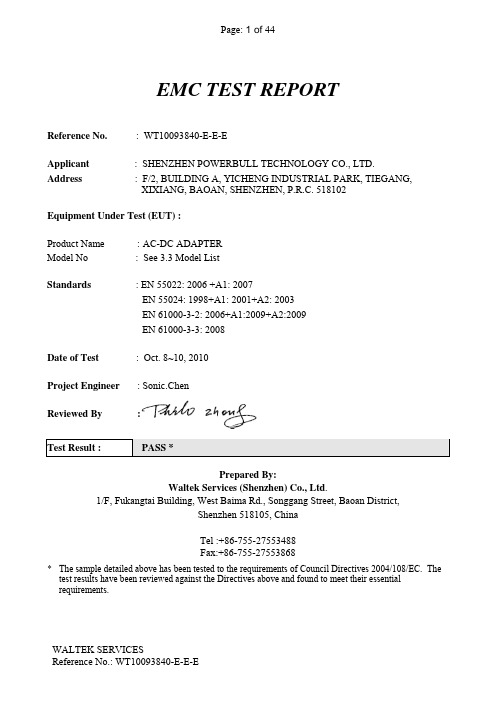
Page: 1 of 44EMC TEST REPORTReference No. : WT10093840-E-E-EApplicant : SHENZHEN POWERBULL TECHNOLOGY CO., LTD.Address : F/2, BUILDING A, YICHENG INDUSTRIAL PARK, TIEGANG,XIXIANG, BAOAN, SHENZHEN, P.R.C. 518102Equipment Under Test (EUT) :Product Name :AC-DC ADAPTERModel No : See 3.3 Model ListStandards : EN 55022: 2006 +A1: 2007EN 55024: 1998+A1: 2001+A2: 2003EN 61000-3-2: 2006+A1:2009+A2:2009EN 61000-3-3: 2008Date of Test: Oct. 8~10, 2010Project Engineer : Sonic.ChenReviewed By :Test Result : PASS *Prepared By:Waltek Services (Shenzhen) Co., Ltd.1/F, Fukangtai Building, West Baima Rd., Songgang Street, Baoan District,Shenzhen 518105, ChinaTel :+86-755-27553488Fax:+86-755-27553868* The sample detailed above has been tested to the requirements of Council Directives 2004/108/EC. The test results have been reviewed against the Directives above and found to meet their essentialrequirements.1Test SummaryTest Test Requirement Test Method Class / Severity ResultMains Terminal Disturbance Voltage, 150kHz to 30MHz EN 55022:2006+A1:2007EN 55022:2006+A1:2007Class B PASSRadiation Emission, 30MHz to 1000MHz EN 55022:2006+A1:2007EN 55022:2006+A1:2007Class B PASSHarmonic Emission on AC, 100Hz to 2kHzEN 61000-3-2:2006+A1:2009+A2:2009EN 61000-3-2:2006+A1:2009+A2:2009Clause 7 ofEN61000-3-2N/AFlicker Emission on AC EN 61000-3-3:2008 EN 61000-3-3:2008Clause 5 ofEN61000-3-3PASSESDEN 55024 : 1998+A1:2001+A2:2003EN 61000-4-2:2009ContactAirPASSRadiated Immunity (80MHz to 1GHz)EN 55024 : 1998+A1:2001+A2:2003EN 61000-4-3:20063V/m, 80%, 1kHz,Amp. Mod.PASSElectrical Fast Transients (EFT) on ACEN 55024 : 1998+A1:2001+A2:2003EN 61000-4-4:2004AC±1.0kVDC±0.5kVPASSSurge Immunity on ACEN 55024 : 1998+A1:2001+A2:2003EN 61000-4-5:2006±1kV D.M.†±2kV C.M.‡PASSInjected Currents on AC, 150kHz to 80MHzEN 55024 : 1998+A1:2001+A2:2003EN61000-4-6:20093Vrms(emf), 80%,1kHz Amp. Mod.PASSPower-frequency magnetic fieldEN 55024 : 1998+A1:2001+A2:2003EN 61000-4-8:1993+A1:20013A/m N/AVoltage Dips and Interruptions on ACEN 55024 : 1998+A1:2001+A2:2003EN 61000-4-11:2004>95 % U T* for0.5per>95 % U T* for250per30 % U T* for 25perPASSRemark:A.M. AmplitudeModulation. P.M. PulseModulation.† D.M. – Differential Modez U T is the nominal supply voltage2ContentsPage 1TEST SUMMARY (2)2CONTENTS (3)3GENERAL INFORMATION (5)3.1C LIENT I NFORMATION (5)3.2G ENERAL D ESCRIPTION OF E.U.T (5)3.3D ETAILS OF E.U.T (5)3.4D ESCRIPTION OF S UPPORT U NITS (10)3.5S TANDARDS A PPLICABLE FOR T ESTING (11)3.6T EST F ACILITY (12)3.7T EST L OCATION (12)4EQUIPMENT USED DURING TEST (13)5EMISSION TEST RESULTS (16)5.1M AINS T ERMINALS D ISTURBANCE V OLTAGE,150K H Z TO 30MH Z (16)5.1.1 E.U.T. Operation (16)5.1.2Conducted Test Setup (16)5.1.3Measurement Data (17)5.1.4Conducted Emissions Test Data (17)5.1.5Photograph– Mains Terminal Disturbance Voltage on AC Test Setup (19)5.2R ADIATION E MISSION D ATA (20)5.2.1 E.U.T. Operation (20)5.2.2Measurement Uncertainty (20)5.2.3Radiated Test Setup (21)5.2.4Spectrum Analyzer Setup (21)5.2.5Test procedure (22)5.2.6Corrected Amplitude & Margin Calculation (22)5.2.7Summary of Test Results (22)5.2.8Radiated Emissions Test Data (23)5.2.9Photograph – Radiation Emission Test Setup (24)5.3H ARMONICS T EST R ESULTS (25)5.4F LICKER T EST R ESULT (26)5.4.1 E.U.T. Operation (26)5.4.2Flicker Test Setup (26)5.4.3Test Data (26)5.4.4Photograph- Flicker Test Setup (27)6IMMUNITY TEST RESULTS (28)6.1P ERFORMANCE C RITERIA D ESCRIPTION (28)6.2ESD (28)6.2.1 E.U.T. Operation (28)6.2.2ESD Test Setup (29)6.2.3Direct Application Test Results (29)6.2.4Indirect Application Test Results (29)6.2.5Photograph - ESD Test Setup (30)6.3R ADIATED I MMUNITY (31)6.3.1 E.U.T. Operation (31)6.3.2Radiated Immunity Test Setup (31)6.3.3Test Results (32)6.3.4Photograph - Radiated Immunity Test Setup (32)6.4E LECTRICAL F AST T RANSIENTS (EFT) (33)6.4.1 E.U.T. Operation (33)6.4.2Electrical Fast Transients Test Setup (33)6.4.3Test Results On AC Cable (33)6.4.4Photograph-EFT Test Setup For EUT On AC Cable (34)6.5S URGE (35)6.5.1 E.U.T. Operation (35)6.5.2Surge Test Setup (35)6.5.3Test Results (35)6.5.4Photograph -Surge Test Setup (36)6.6C ONDUCTED I MMUNITY 0.15MH Z TO 80MH Z (37)6.6.1 E.U.T. Operation (37)6.6.2Conducted Immunity Test Setup (37)6.6.3Test Results AC mains of EUT (37)6.6.4Photograph - Conducted Immunity Test Setup On AC Cable (38)6.7V OLTAGE D IPS AND I NTERRUPTIONS (39)6.7.1 E.U.T. Operation (39)6.7.2Voltage Dips and Interruptions Test Setup (39)6.7.3Measurement Data (39)6.7.4Photograph - Voltage Dips and Interruptions Test Setup (40)7PHOTOGRAPHS - CONSTRUCTIONAL DETAILS (41)7.1EUT–F RONT V IEW (41)7.2EUT–S IDE V IEW (41)7.3EUT–O PEN V IEW (42)7.4PCB–T OP V IEW (43)7.5PCB–B OTTOM V IEW (43)8CE LABEL (44)3 General Information3.1 Client InformationApplicant : SHENZHEN POWERBULL TECHNOLOGY CO., LTD. Address of Applicant : F/2, BUILDING A, YICHENG INDUSTRIAL PARK,TIEGANG, XIXIANG, BAOAN, SHENZHEN P.R.C. 518102Manufacturer : SHENZHEN POWERBULL TECHNOLOGY CO., LTD. Address of Manufacturer: F/2, BUILDING A, YICHENG INDUSTRIAL PARK,TIEGANG, XIXIANG, BAOAN, SHENZHEN, P.R.C. 518102 3.2 General Description of E.U.T.Product Name : AC-DC ADAPTER Model No. : See 3.3 Model ListModel Description: All models have the same schematic and PCB layoutexcept for output voltage. The mode LN-2400050-AW, LN-1390080-AW and LN-0750160-AW were the test sample. 3.3 Details of E.U.T.Model ListOUTPUT Rating MODELINPUT RatingV/ A V A LN-0720160-AW AC100-240V 50/60Hz 0.35A 7.2 1.6 LN-0730160-AW AC100-240V 50/60Hz 0.35A 7.3 1.6 LN-0740160-AW AC100-240V 50/60Hz 0.35A 7.4 1.6 LN-0750160-AW AC100-240V 50/60Hz 0.35A 7.5 1.6 LN-0760150-AW AC100-240V 50/60Hz 0.35A 7.6 1.5 LN-0770150-AW AC100-240V 50/60Hz 0.35A 7.7 1.5 LN-0780150-AW AC100-240V 50/60Hz 0.35A 7.8 1.5 LN-0790150-AW AC100-240V 50/60Hz 0.35A 7.9 1.5 LN-0800150-AW AC100-240V 50/60Hz 0.35A 8.0 1.5 LN-0810140-AW AC100-240V 50/60Hz 0.35A 8.1 1.4 LN-0820140-AW AC100-240V 50/60Hz 0.35A 8.2 1.4 LN-0830140-AW AC100-240V 50/60Hz 0.35A 8.3 1.4 LN-0840140-AWAC100-240V 50/60Hz 0.35A8.41.4LN-0850140-AW AC100-240V 50/60Hz 0.35A 8.5 1.4 LN-0860140-AW AC100-240V 50/60Hz 0.35A 8.6 1.4 LN-0870130-AW AC100-240V 50/60Hz 0.35A 8.7 1.3 LN-0880130-AW AC100-240V 50/60Hz 0.35A 8.8 1.3 LN-0890130-AW AC100-240V 50/60Hz 0.35A 8.9 1.3 LN-0900130-AW AC100-240V 50/60Hz 0.35A 9.0 1.3 LN-0910130-AW AC100-240V 50/60Hz 0.35A 9.1 1.3 LN-0920130-AW AC100-240V 50/60Hz 0.35A 9.2 1.3 LN-0930130-AW AC100-240V 50/60Hz 0.35A 9.3 1.3 LN-0940120-AW AC100-240V 50/60Hz 0.35A 9.4 1.2 LN-0950120-AW AC100-240V 50/60Hz 0.35A 9.5 1.2 LN-0960120-AW AC100-240V 50/60Hz 0.35A 9.6 1.2 LN-0970120-AW AC100-240V 50/60Hz 0.35A 9.7 1.2 LN-0980120-AW AC100-240V 50/60Hz 0.35A 9.8 1.2 LN-0990120-AW AC100-240V 50/60Hz 0.35A 9.9 1.2 LN-1000120-AW AC100-240V 50/60Hz 0.35A 10.0 1.2 LN-1010110-AW AC100-240V 50/60Hz 0.35A 10.1 1.1 LN-1010110-AW AC100-240V 50/60Hz 0.35A 10.2 1.1 LN-1030110-AW AC100-240V 50/60Hz 0.35A 10.3 1.1 LN-1040110-AW AC100-240V 50/60Hz 0.35A 10.4 1.1 LN-1050110-AW AC100-240V 50/60Hz 0.35A 10.5 1.1 LN-1060110-AW AC100-240V 50/60Hz 0.35A 10.6 1.1 LN-1070110-AW AC100-240V 50/60Hz 0.35A 10.7 1.1 LN-1080110-AW AC100-240V 50/60Hz 0.35A 10.8 1.1 LN-1090110-AW AC100-240V 50/60Hz 0.35A 10.9 1.1 LN-1100100-AW AC100-240V 50/60Hz 0.35A 11.0 1.0 LN-1110100-AW AC100-240V 50/60Hz 0.35A 11.1 1.0 LN-1120100-AW AC100-240V 50/60Hz 0.35A 11.2 1.0 LN-1130100-AW AC100-240V 50/60Hz 0.35A 11.3 1.0 LN-1140100-AW AC100-240V 50/60Hz 0.35A 11.4 1.0 LN-1150100-AW AC100-240V 50/60Hz 0.35A 11.5 1.0 LN-1160100-AW AC100-240V 50/60Hz 0.35A 11.6 1.0 LN-1170100-AW AC100-240V 50/60Hz 0.35A 11.7 1.0 LN-1180100-AW AC100-240V 50/60Hz 0.35A 11.8 1.0 LN-1190100-AW AC100-240V 50/60Hz 0.35A 11.9 1.0LN-1200100-AW AC100-240V 50/60Hz 0.35A 12.0 1.0 LN-1210090-AW AC100-240V 50/60Hz 0.35A 12.1 0.9 LN-1220090-AW AC100-240V 50/60Hz 0.35A 12.2 0.9 LN-1230090-AW AC100-240V 50/60Hz 0.35A 12.3 0.9 LN-1240090-AW AC100-240V 50/60Hz 0.35A 12.4 0.9 LN-1250090-AW AC100-240V 50/60Hz 0.35A 12.5 0.9 LN-1260090-AW AC100-240V 50/60Hz 0.35A 12.6 0.9 LN-1270090-AW AC100-240V 50/60Hz 0.35A 12.7 0.9 LN-1280090-AW AC100-240V 50/60Hz 0.35A 12.8 0.9 LN-1290090-AW AC100-240V 50/60Hz 0.35A 12.9 0.9 LN-1300090-AW AC100-240V 50/60Hz 0.35A 13.0 0.9 LN-1310090-AW AC100-240V 50/60Hz 0.35A 13.1 0.9 LN-1320090-AW AC100-240V 50/60Hz 0.35A 13.2 0.9 LN-1330090-AW AC100-240V 50/60Hz 0.35A 13.3 0.9 LN-1340090-AW AC100-240V 50/60Hz 0.35A 13.4 0.9 LN-1350080-AW AC100-240V 50/60Hz 0.35A 13.5 0.8 LN-1360080-AW AC100-240V 50/60Hz 0.35A 13.6 0.8 LN-1370080-AW AC100-240V 50/60Hz 0.35A 13.7 0.8 LN-1380080-AW AC100-240V 50/60Hz 0.35A 13.8 0.8 LN-1390080-AW AC100-240V 50/60Hz 0.35A 13.9 0.8 LN-1400080-AW AC100-240V 50/60Hz 0.35A 14.0 0.8 LN-1410080-AW AC100-240V 50/60Hz 0.35A 14.1 0.8 LN-1420080-AW AC100-240V 50/60Hz 0.35A 14.2 0.8 LN-1430080-AW AC100-240V 50/60Hz 0.35A 14.3 0.8 LN-1440080-AW AC100-240V 50/60Hz 0.35A 14.4 0.8 LN-1450080-AW AC100-240V 50/60Hz 0.35A 14.5 0.8 LN-1460080-AW AC100-240V 50/60Hz 0.35A 14.6 0.8 LN-1470080-AW AC100-240V 50/60Hz 0.35A 14.7 0.8 LN-1480080-AW AC100-240V 50/60Hz 0.35A 14.8 0.8 LN-1490080-AW AC100-240V 50/60Hz 0.35A 14.9 0.8 LN-1500080-AW AC100-240V 50/60Hz 0.35A 15.0 0.8 LN-1510070-AW AC100-240V 50/60Hz 0.35A 15.1 0.7 LN-1520070-AW AC100-240V 50/60Hz 0.35A 15.2 0.7 LN-1530070-AW AC100-240V 50/60Hz 0.35A 15.3 0.7 LN-1540070-AW AC100-240V 50/60Hz 0.35A 15.4 0.7LN-1550070-AW AC100-240V 50/60Hz 0.35A 15.5 0.7 LN-1560070-AW AC100-240V 50/60Hz 0.35A 15.6 0.7 LN-1570070-AW AC100-240V 50/60Hz 0.35A 15.7 0.7 LN-1580070-AW AC100-240V 50/60Hz 0.35A 15.8 0.7 LN-1590070-AW AC100-240V 50/60Hz 0.35A 15.9 0.7 LN-1600070-AW AC100-240V 50/60Hz 0.35A 16.0 0.7 LN-1610070-AW AC100-240V 50/60Hz 0.35A 16.1 0.7 LN-1620070-AW AC100-240V 50/60Hz 0.35A 16.2 0.7 LN-1630070-AW AC100-240V 50/60Hz 0.35A 16.3 0.7 LN-1640070-AW AC100-240V 50/60Hz 0.35A 16.4 0.7 LN-1650070-AW AC100-240V 50/60Hz 0.35A 16.5 0.7 LN-1660070-AW AC100-240V 50/60Hz 0.35A 16.6 0.7 LN-1670070-AW AC100-240V 50/60Hz 0.35A 16.7 0.7 LN-1680070-AW AC100-240V 50/60Hz 0.35A 16.8 0.7 LN-1690070-AW AC100-240V 50/60Hz 0.35A 16.9 0.7 LN-1700070-AW AC100-240V 50/60Hz 0.35A 17.0 0.7 LN-1710070-AW AC100-240V 50/60Hz 0.35A 17.1 0.7 LN-1720070-AW AC100-240V 50/60Hz 0.35A 17.2 0.7 LN-1730060-AW AC100-240V 50/60Hz 0.35A 17.3 0.6 LN-1740060-AW AC100-240V 50/60Hz 0.35A 17.4 0.6 LN-1750060-AW AC100-240V 50/60Hz 0.35A 17.5 0.6 LN-1760060-AW AC100-240V 50/60Hz 0.35A 17.6 0.6 LN-1770060-AW AC100-240V 50/60Hz 0.35A 17.7 0.6 LN-1780060-AW AC100-240V 50/60Hz 0.35A 17.8 0.6 LN-1790060-AW AC100-240V 50/60Hz 0.35A 17.9 0.6 LN-1800060-AW AC100-240V 50/60Hz 0.35A 18.0 0.6 LN-1810060-AW AC100-240V 50/60Hz 0.35A 18.1 0.6 LN-1820060-AW AC100-240V 50/60Hz 0.35A 18.2 0.6 LN-1830060-AW AC100-240V 50/60Hz 0.35A 18.3 0.6 LN-1840060-AW AC100-240V 50/60Hz 0.35A 18.4 0.6 LN-1850060-AW AC100-240V 50/60Hz 0.35A 18.5 0.6 LN-1860060-AW AC100-240V 50/60Hz 0.35A 18.6 0.6 LN-1870060-AW AC100-240V 50/60Hz 0.35A 18.7 0.6 LN-1880060-AW AC100-240V 50/60Hz 0.35A 18.8 0.6 LN-1890060-AW AC100-240V 50/60Hz 0.35A 18.9 0.6LN-1900060-AW AC100-240V 50/60Hz 0.35A 19.0 0.6 LN-1910060-AW AC100-240V 50/60Hz 0.35A 19.1 0.6 LN-1920060-AW AC100-240V 50/60Hz 0.35A 19.2 0.6 LN-1930060-AW AC100-240V 50/60Hz 0.35A 19.3 0.6 LN-1940060-AW AC100-240V 50/60Hz 0.35A 19.4 0.6 LN-1950060-AW AC100-240V 50/60Hz 0.35A 19.5 0.6 LN-1960060-AW AC100-240V 50/60Hz 0.35A 19.6 0.6 LN-1970060-AW AC100-240V 50/60Hz 0.35A 19.7 0.6 LN-1980060-AW AC100-240V 50/60Hz 0.35A 19.8 0.6 LN-1990060-AW AC100-240V 50/60Hz 0.35A 19.9 0.6 LN-2000060-AW AC100-240V 50/60Hz 0.35A 20.0 0.6 LN-2010050-AW AC100-240V 50/60Hz 0.35A 20.1 0.5 LN-2020050-AW AC100-240V 50/60Hz 0.35A 20.2 0.5 LN-2030050-AW AC100-240V 50/60Hz 0.35A 20.3 0.5 LN-2040050-AW AC100-240V 50/60Hz 0.35A 20.4 0.5 LN-2050050-AW AC100-240V 50/60Hz 0.35A 20.5 0.5 LN-2060050-AW AC100-240V 50/60Hz 0.35A 20.6 0.5 LN-2070050-AW AC100-240V 50/60Hz 0.35A 20.7 0.5 LN-2080050-AW AC100-240V 50/60Hz 0.35A 20.8 0.5 LN-2090050-AW AC100-240V 50/60Hz 0.35A 20.9 0.5 LN-2100050-AW AC100-240V 50/60Hz 0.35A 21.0 0.5 LN-2110050-AW AC100-240V 50/60Hz 0.35A 21.1 0.5 LN-2120050-AW AC100-240V 50/60Hz 0.35A 21.2 0.5 LN-2130050-AW AC100-240V 50/60Hz 0.35A 21.3 0.5 LN-2140050-AW AC100-240V 50/60Hz 0.35A 21.4 0.5 LN-2150050-AW AC100-240V 50/60Hz 0.35A 21.5 0.5 LN-2160050-AW AC100-240V 50/60Hz 0.35A 21.6 0.5 LN-2170050-AW AC100-240V 50/60Hz 0.35A 21.7 0.5 LN-2180050-AW AC100-240V 50/60Hz 0.35A 21.8 0.5 LN-2190050-AW AC100-240V 50/60Hz 0.35A 21.9 0.5 LN-2200050-AW AC100-240V 50/60Hz 0.35A 22.0 0.5 LN-2210050-AW AC100-240V 50/60Hz 0.35A 22.1 0.5 LN-2220050-AW AC100-240V 50/60Hz 0.35A 22.2 0.5 LN-2230050-AW AC100-240V 50/60Hz 0.35A 22.3 0.5 LN-2240050-AW AC100-240V 50/60Hz 0.35A 22.4 0.5LN-2250050-AW AC100-240V 50/60Hz 0.35A 22.5 0.5LN-2260050-AW AC100-240V 50/60Hz 0.35A 22.6 0.5LN-2270050-AW AC100-240V 50/60Hz 0.35A 22.7 0.5LN-2280050-AW AC100-240V 50/60Hz 0.35A 22.8 0.5LN-2290050-AW AC100-240V 50/60Hz 0.35A 22.9 0.5LN-2300050-AW AC100-240V 50/60Hz 0.35A 23.0 0.5LN-2310051-AW AC100-240V 50/60Hz 0.35A 23.1 0.5LN-2320050-AW AC100-240V 50/60Hz 0.35A 23.2 0.5LN-2330050-AW AC100-240V 50/60Hz 0.35A 23.3 0.5LN-2340050-AW AC100-240V 50/60Hz 0.35A 23.4 0.5LN-2350050-AW AC100-240V 50/60Hz 0.35A 23.5 0.5LN-2360050-AW AC100-240V 50/60Hz 0.35A 23.6 0.5LN-2370050-AW AC100-240V 50/60Hz 0.35A 23.7 0.5LN-2380050-AW AC100-240V 50/60Hz 0.35A 23.8 0.5LN-2390050-AW AC100-240V 50/60Hz 0.35A 23.9 0.5LN-2400050-AW AC100-240V 50/60Hz 0.35A 24.0 0.5--THE END--3.4Description of Support UnitsThe resistor is the support unit.3.5Standards Applicable for TestingThe customer requested EMC tests for an AC-DC ADAPTER. The standards used wereEN55022 for emissions & EN55024 for immunity, and EN 61000-3-2,EN 61000-3-3 forHarmonic and Flicker..Table 1 : Tests Carried Out Under EN 55022: 2006+A1:2007Standard Status EN 55022:2006+A1:2007 Radiation Emission, 30MHz to 1000MHz √EN 55022:2006+A1:2007 Mains Terminal Disturbance Voltage,150KHz to 30MHz √Table 2 : Tests Carried Out Under EN 61000-3-2: 2006+A1:2009+A2:2009 & EN 61000-3-3:2008EN 61000-3-2: 2006+A1:2009+A2:2009 Harmonic Emissions on AC ×EN 61000-3-3:2008 Flicker Emissions on AC √Table 3 : Tests Carried Out Under EN 55024:1998+A1:2001+A2: 2003Standard Status EN 61000-4-2:2009 Electro-static discharge √EN 61000-4-3:2006 Radio frequency EM fields (80MHz to 1GHz) √EN 61000-4-4:2004 Fast transients √EN 61000-4-5:2006 Surges √EN 61000-4-6: 2009 Radio frequency continuous conducted (150kHz to 80MHz) √EN 61000-4-8:1993+A1:2001 Power-frequency magnetic field (50Hz) ×EN 61000-4-11:2004 Voltage dips & interruptions √√Indicates that the test is applicable×Indicates that the test is not applicable3.6Test FacilityThe test facility is recognized, certified, or accredited by the following organizations:• IC – Registration No.: 7760AWaltek Services(Shenzhen) Co., Ltd. has been registered and fully described in a report filed with the Industry Canada. The acceptance letter from the Industry Canada is maintained in our files. Registration 7760A, Aug 03, 2010.•FCC – Registration No.: 880581Waltek Services(Shenzhen) Co., Ltd. EMC Laboratory has been registered and fullydescribed in a report filed with the (FCC) Federal Communications Commission. Theacceptance letter from the FCC is maintained in our files. Registration 880581, June 24, 2008.3.7Test LocationAll the tests were performed at:-Waltek Services(Shenzhen) Co., Ltd. at 1/F, Fukangtai Building, West Baima Rd.,Songgang Street, Baoan District, Shenzhen, China4Equipment Used during TestEquipment Name ManufacturerModelEquipment NoInternal No SpecificationCal.DateDueDateCert. No UncertaintyEMC Analyzer Agilent/E7405AMY45114943W2008001 9k-26.5GHz Aug-10Aug-11Wws20081596±1dBTrilog Broadband Antenne 30-3000 MHz SCHWARZBECK MESS-ELEKTROM/VULB9163336W2008002 30-3000MHz Aug-10Aug-11 - ±1dBBroad-band Horn Antenna 1-18 GHz SCHWARZBECK MESS-ELEKTROM/VULB9163667W2008003 1-18GHz Aug-10Aug-11 -f<10GHz:±1dB10GHz<f<18 GHz:±1.5dBBroadband Preamplifier 0.5-18 GHz SCHWARZBECK MESS-ELEKTROM/BBV 97189718-148W2008004 0.5-18GHz Aug-10Aug-11 - ±1.2dB10m Coaxial Cable with N-male Connectors usable up to 18GHz, SCHWARZBECK MESS-ELEKTROM/AK 9515 H-- - Aug-10Aug-11--10m 50 Ohm Coaxial Cable with N-plug, individual length, usable up to 3(5)GHz, Connector SCHWARZBECK MESS-ELEKTROM/AK 9513- - - Aug-10Aug-11- -Positioning Controller C&C LAB/CC-C-IF-- - N/AN/A--Color Monitor SUNSPO/ SP-14C-- - N/AN/A--Test Receiver ROHDE&SCHWARZ/ESPI101155W2005001 9k-3GHz Aug-10Aug-11Wws20080942±1dBEMI Receiver Beijingkehuan KH3931- 9k-1GHzAug-10Aug-11--Two-Line V-Network ROHDE&SCHWARZ/ENV216100115W2005002 50Ω/50μΗ Aug-10Aug-11Wws20080941±10%Absorbing Clamp ROHDE&SCHWARZ/MDS-21100205 W2005003 impandance50Ωloss:17 dBAug-10Aug-11Wws20080943±1dBEquipment Name ManufacturerModelEquipment NoInternal No SpecificationCal.DateDueDateCert. No Uncertainty10m 50 Ohm Coaxial Cable with N-plug, individual length, usable up to 3(5)GHz, Connectors SCHWARZBECK MESS-ELEKTROM/AK 9514- - - Aug-10Aug-11- -Digital Power Analyzer Em TestAG/Switzerland/ DPA 500V0745103095W2008012Power:2000VAVol-range:0-300VFreq_range:10-80HzPower Source Em TestAG/Switzerland/ ACS 500V0745103096W2008013Vol-range:0-300VPower_freq:10-80HzAug-10Aug-11Wwd20081185Voltagedistinguish:0.025%Power_freqdistinguish:0.02HzElectrostatic Discharge Simulator Em TestAG/Switzerland/DITOV0745103094W2008005Contactdischarge:500V-10KVAirdiacharge:500V-16.5KVAug-10Aug-11Wwc200824007.5A currentwill bechanged inV m=1.5VRF Generator TESEQGmbH/NSG407025781W2008008Fraq-range:9K-1GHzRF voltage:-60 dBm-+10dBmAug-10Aug-11Wws20081890Power_freqdistinguish0.1HzRFeletricitydistinguish0.1BCDN M-Type TESEQGmbH/ CDNM01625112W2008009Voltagecorrect factor9.5 dBAug-10Aug-11Wwc20082396150K-80MHz:±1dB80-230MHz:-2-+3dBEM-Clamp TESEQGmbH/KEMZ 801 25453W2008010Freq_range:0.15-1000MHzAug-10Aug-11Wwc200823970.3-400MHz:±4dBOther freq:±5dBAttenuator 6dB TESEQGmbH/ATN605025365Aug-10Aug-11Wws20081597All Modules GeneratorSCHAFFNER /6150 34579 W2008006voltage:200V-4.4KVPulsecurrent:100A-2.2KAAug-10Aug-11Wwc20082401voltage:±10%Pulsecurrent:±10%Equipment Name ManufacturerModelEquipment NoInternal No SpecificationCal.DateDueDateCert. No UncertaintyCapacitive Coupling Clamp SCHAFFNER/ CDN 801425311Aug-10Aug-11Wwc20082398-Signal and Data Line Coupling Network SCHAFFNER/ CDN 11725627W20080111.2/50μSAug-10Aug-11Wwc20082399-AC Power Supply TONGYUN/DTDGC-4Aug-10Aug-11Wws20080944-Exposure Level Tester ELT-400 Narda SafetyTESTSolutions/2304/03M-0155 w2008022Test freqrange:1-400kHzTestuncertainly:1-120kHz:±1.83%,120 kHz-400kHz:±4.06%Magnetic Field Probe 100cm2 Narda SafetyTESTSolutions/2300/90.10M-1070w2008021Test freqrange:1-400kHzAug-10Aug-11Wwd20081191 Testuncertainly:1Hz-10Hz:±16.2%,10Hz -120kHz:±2.2%,120 kHz-400kHz: ±4.7%Active LoopAntenna Charger 10kHz-30MHz Beijing Dazhi/ ZN30900A- -10kHz-30MHzAug-10Aug-11 - ±1dB5Emission Test Results5.1Mains Terminals Disturbance Voltage, 150kHz to 30MHzTest Requirement: EN 55022 Class BTest Method: EN 55022 Class BTest Result: PASSFrequency Range: 150kHz to 30MHzBClass/Severity: ClassDetector: Peak for pre-scan (9kHz Resolution Bandwidth)Quasi-Peak & Average if maximised peak within 6dB of AverageLimit5.1.1E.U.T. OperationOperating Environment:°CTemperature: 25.5Humidity: 51 % RHAtmospheric Pressure: 1012 mbarEUT Operation :Compliance test was performed in working mode with full load,half load and no load.fullload is the worst mode.below shows the mode data.The maximised peak emissions from the EUT was scanned and measured for both the Live and Neutral Lines. Quasi-peak & average measurements were performed if peak emissions were within 6dB of the average limit line.5.1.2Conducted Test SetupThe conducted emission tests were performed using the setup accordance with the EN55022:2006+A1:2007, The specification used in this report was the EN 55022:2006+A1:2007 Paragraph 5 limits.5.1.3Measurement DataAn initial pre-scan was performed on the live and neutral lines.No futher quasi-peak or average measurements were performed since no peak emissions were detected within 10dB line below the average limit.Please refer to the following peak scan graph for reference.5.1.4Conducted Emissions Test DataM/N:LN-1390080-AW(the worst model) Mode:Full load mode(the worst mode)Live Line:Neutral Line:5.1.5Photograph– Mains Terminal Disturbance Voltage on AC Test Setup5.2Radiation Emission DataTest Requirement: EN 55022 Class BTest Method: EN 55022 Class BTest Result: PASSFrequency Range: 30MHz to 1000MHzBClass/Severity: ClassDetector: Peak for pre-scan (120KHz Resolution Bandwidth)Quasi-Peak & Average if maximised peak within 6dB of AverageLimit5.2.1E.U.T. OperationOperating Environment:°CTemperature: 25.5Humidity: 51 % RHAtmospheric Pressure: 1012 mbarEUT Operation :Compliance test was performed in working mode with full load,half load and no load.full load is the worst mode.below shows the mode data.5.2.2Measurement UncertaintyAll measurements involve certain levels of uncertainties, especially in the field of EMC. The factors contributing to uncertainties are spectrum analyzer, cable loss, antenna factorcalibration, antenna directivity, antenna factor variation with height, antenna phase centervariation, antenna factor frequency interpolation, measurement distance variation, siteimperfections, mismatch (average), and system repeatability.Based on CISPR16-4-2, The Treatment of Uncertainty in EMC Measurements, the bestestimate of the uncertainty of a radiation emissions measurement at Waltek EMC Lab is+5.03 dB.5.2.3Radiated Test SetupThe radiated emission tests were performed in the 3m Semi- Anechoic Chamber test site,using the setup accordance with the EN 55022:2006+A1:2007, The specification used in this report was the EN 55022:2006+A1:2007Paragraph 6 limits.5.2.4Spectrum Analyzer SetupAccording to EN55022 Class B Rules, the system was tested to 1000 MHz.Start Frequency..............................................30 MHzStop Frequency..............................................1000 MHzSweep Speed AutoIF Bandwidth.............................................120KHzVideo Bandwidth...........................................100KHzQuasi-Peak Adapter Bandwidth....................120 KHzQuasi-Peak Adapter Mode............................NormalResolution Bandwidth...................................100KHz5.2.5Test procedureFor the radiated emissions test, maximizing procedure was performed on the six (6) highest emissions to ensure EUT is compliant with all installation combinations.All data was recorded in the peak detection mode. Quasi-peak readings was performed only when an emission was found to be marginal (within +/-4 dBμV of specification limits), and are distinguished with a "Qp" in the data table.The EUT was under normal mode during the final qualification test and the configuration was used to represent the worst case results.5.2.6Corrected Amplitude & Margin CalculationThe Corrected Amplitude is calculated by adding the Antenna Factor and Cable Factor, and subtracting the Amplifier Gain from the Amplitude reading. The basic equation is as follows:Corr. Ampl. = Indicated Reading + Antenna Factor + Cable Factor - Amplifier GainThe “Margin” column of the following data tables indicates the degree of compliance with the applicable limit. For example, a margin of -7dBμV means the emission is 7dBμV below the maximum limit for Class B. The equation for margin calculation is as follows:Margin = Corr. Ampl. – Class B Limit5.2.7Summary of Test ResultsAccording to the data in section 5.2.8, the EUT complied with the EN55022 Class B standards.5.2.8Radiated Emissions Test DataM/N:LN-1390080-AW(the worst model) Mode:Full load mode(the worst mode) Antenna Polarization:VerticalAntenna Polarization:Horizontal5.2.9Photograph – Radiation Emission Test Setup5.3Harmonics Test ResultsTest Requirement: EN61000-3-2Test Method: EN61000-3-2Frequency Range: 100Hz to 2kHzTest Result: N/AFor further details, please refer to Clause 7, Note 1 of EN61000-3-2 which states:-“For the following categories of equipment limits are not specified in this edition of the standard.Note 1: Equipment with a rated power of 75W or less, other than lighting equipment.”5.4Flicker Test ResultTest Requirement: EN61000-3-3Test Method: EN61000-3-3Test Result PASS5.4.1E.U.T. OperationOperating Environment:°CTemperature: 25.5Humidity: 51 % RHAtmospheric Pressure: 1012 mbarEUT Operation :Compliance test was performed in working mode with full load,half load and no load.full load is the worst mode.below shows the mode data.5.4.2Flicker Test SetupThe Flicker Test steup accordance with the EN 61000-3-3, The Specificationused in this report was the EN61000-3-3 Paragraph 5 limits.5.4.3Test DataM a x i m u m F l i c k e r r e s u l t sEUT values Limit ResultPASS1.00Pst 0.0540.65PASSPlt 0.054dc [%] 0.004 3.30 PASSdmax [%] 0.269 4.00 PASSdt [s] 0.000 0.50 PASS5.4.4Photograph- Flicker Test Setup6Immunity Test Results6.1Performance Criteria DescriptionCriterion A: The apparatus shall continue to operate as intended. No degradation ofperformance or loss of function is allowed below a performance level specified bythe manufacturer, when the apparatus is used as intended.Criterion B: The apparatus shall continue to operate as intended after the test. No degradation of performance or loss of function is allowed below a performance level specifiedby the manufacturer, when the apparatus is used as intended.Criterion C: Temporary loss of function is allowed, provided the function is self recoverable or can be restored by the operation of the controls.For further details, please refer to EN55024.6.2ESDTest Requirement: EN55024Test Method: EN61000-4-2Test Result: PASSDischarge Impedance: 330 Ω / 150 pFDischarge Voltage: Air Discharge: +/- 8 kVContact Discharge: +/- 4 kVHCP & VCP: +/- 4 kVPolarity: Positive & NegativeNumber of Discharge: Minimum 10 times at each test pointDischarge Mode: Single DischargeDischarge Period: 1 second minimum6.2.1 E.U.T. OperationOperating Environment:Temperature : 25.5 °CHumidity : 51 % RHBarometric Pressure : 1012 mbarEUT Operation:Compliance test was performed in working mode with full load mode.。

一、概述伯乐超敏成像仪(Belle Ultra-Sensitive Imager,简称BUI)是一款高性能、高灵敏度的荧光成像设备,广泛应用于生命科学、材料科学、生物医学等领域。
该成像仪采用先进的光学系统、高分辨率CCD相机和强大的图像处理软件,实现了对生物样品、材料样品等低光信号的高灵敏度成像。
二、主要技术参数1. 成像模式BUI支持多种成像模式,包括:(1)荧光成像:适用于观察荧光标记的细胞、组织、蛋白质等生物样品。
(2)化学发光成像:适用于观察化学发光标记的样品。
(3)共聚焦成像:适用于观察活细胞、组织切片等样品。
(4)共聚焦扫描激光扫描共聚焦显微镜成像:适用于观察三维结构样品。
2. 成像分辨率BUI采用高性能CCD相机,可实现以下成像分辨率:(1)荧光成像:500万像素,分辨率可达0.4μm。
(2)化学发光成像:500万像素,分辨率可达0.4μm。
(3)共聚焦成像:500万像素,分辨率可达0.4μm。
(4)共聚焦扫描激光扫描共聚焦显微镜成像:500万像素,分辨率可达0.4μm。
3. 灵敏度BUI具有极高的灵敏度,可实现以下成像灵敏度:(1)荧光成像:最低信噪比可达1000:1。
(2)化学发光成像:最低信噪比可达1000:1。
(3)共聚焦成像:最低信噪比可达1000:1。
(4)共聚焦扫描激光扫描共聚焦显微镜成像:最低信噪比可达1000:1。
4. 线性范围BUI具有较宽的线性范围,可实现以下成像线性范围:(1)荧光成像:线性范围可达10,000:1。
(2)化学发光成像:线性范围可达10,000:1。
(3)共聚焦成像:线性范围可达10,000:1。
(4)共聚焦扫描激光扫描共聚焦显微镜成像:线性范围可达10,000:1。
5. 照度范围BUI具有较宽的照度范围,可实现以下成像照度范围:(1)荧光成像:照度范围可达0.1-100,000 photons/s。
(2)化学发光成像:照度范围可达0.1-100,000 photons/s。

第43卷㊀第1期2022年1月发㊀光㊀学㊀报CHINESE JOURNAL OF LUMINESCENCEVol.43No.1Jan.,2022㊀㊀收稿日期:2021-10-25;修订日期:2021-11-11㊀㊀基金项目:国家重点研发计划(2017YFB0404104);国家自然科学基金(61974139);北京自然科学基金(4182063)资助项目Supported by National Key R&D Program of China (2017YFB0404104);National Natural Science Foundation of China (61974139);Beijing Natural Science Foundation(4182063)文章编号:1000-7032(2022)01-0001-07量子垒高度对深紫外LED 调制带宽的影响郭㊀亮1,2,郭亚楠1,2,羊建坤1,2,闫建昌1,2,王军喜1,2,魏同波1,2∗(1.中国科学院半导体研究所半导体照明研发中心,北京㊀100083;2.中国科学院大学材料与光电研究中心,北京㊀100049)摘要:AlGaN 基深紫外LED 由于具有高调制带宽和小芯片尺寸,在紫外光通信领域受到越来越多的关注㊂本研究通过改变生长AlGaN 量子垒层的Al 源流量,生长了三种具有不同量子垒高度的深紫外LED,研究了量子垒高度对深紫外LED 光电特性和调制特性的影响㊂研究发现,随着量子垒高度的增加,深紫外LED 的光功率出现先增加后减小的趋势,量子垒中Al 组分为55%的深紫外LED 的光功率相比50%和60%的深紫外LED 提升了近一倍㊂载流子寿命则出现先减小后增大的趋势,且发光峰峰值波长逐渐蓝移㊂APSYS 模拟表明,随着量子垒高度增加,量子垒对载流子的束缚能力增强,电子空穴波函数空间重叠增加,载流子浓度和辐射复合速率增加;但进一步增加量子垒高度又会由于电子泄露,空穴浓度降低,从而辐射复合速率降低㊂量子垒中Al 组分为55%的深紫外LED 的-3dB 带宽达到94.4MHz,高于量子垒Al 组分为50%和60%的深紫外LED㊂关㊀键㊀词:紫外光通信;深紫外发光二极管;多量子阱层;调制带宽;发光功率中图分类号:TN383+.1;TN929.12㊀㊀㊀文献标识码:A㊀㊀㊀DOI :10.37188/CJL.20210331Effect of Barrier Height on Modulation Characteristics ofAlGaN-based Deep Ultraviolet Light-emitting DiodesGUO Liang 1,2,GUO Ya-nan 1,2,YANG Jian-kun 1,2,YAN Jian-chang 1,2,WANG Jun-xi 1,2,WEI Tong-bo 1,2∗(1.Research and Development Center for Semiconductor Lighting Technology ,Institute of Semiconductors ,Chinese Academy of Sciences ,Beijing 100083,China ;2.Center of Materials Science and Optoelectronics Engineering ,University of Chinese Academy of Sciences ,Beijing 100049,China )∗Corresponding Author ,E-mail :tbwei @Abstract :AlGaN-based deep ultraviolet LED has attracted more and more attention in ultravioletcommunication due to its high modulation bandwidth and small chip size.In this study,AlGaN-based deep ultraviolet LEDs with varied Al composition of 50%,55%,60%in quantum barriers are fabricated.The effect of barrier height on the photoelectric and modulation characteristics of deep ultraviolet LEDs is studied.It is found that the optical power and external quantum efficiency (EQE)of the deep ultraviolet LED increase first and then decreased,and carrier lifetime decreases first and then increases as the quantum barrier height increases.The peak wavelength of the spectra shows a blue-shift.APSYS simulation revealed that the spacial overlap between the wave function of electron and hole is enhanced as Al composition increases.But further increase on barrier height will lead to current leakage which reduces the radiation recombination rate and carrier density in . All Rights Reserved.2㊀发㊀㊀光㊀㊀学㊀㊀报第43卷quantum well layer.The-3dB bandwidth of deep ultraviolet LED with55%Al composition inquantum barrier is measured to be94.4MHz,higher than those with50%and60%Al composition in quantum barrier.Key words:ultraviolet communication;deep ultraviolet light-emitting diodes;multiple-quantum-well layer;modula-tion bandwidth;optical power1㊀引㊀㊀言随着深紫外LED和日盲探测器的发展,紫外光通信受到越来越多的关注㊂紫外光通信利用紫外光传输信号,该信号可以被漂浮在空气中的微粒和气溶胶等散射和反射,实现非视距通信[1-2]㊂紫外光通信中使用的紫外光也称为日盲紫外光,它在光谱中位于200~280nm之间[3-4]㊂当太阳辐射穿过大气层时,会被空气中的水蒸气㊁二氧化碳㊁氧气㊁臭氧㊁悬浮颗粒和其他气体分子强烈散射㊁吸收或反射,从而导致太阳光谱不连续㊂在所有分子和粒子中,仅占大气0.01%~0.1%的臭氧在紫外光谱中具有很强的吸收带,从而使得到达地表的太阳光中日盲紫外光含量极少,这则为紫外光通信提供了低背景噪声的通信环境[5]㊂同时,紫外光通信还具有高保密性㊁无需频段许可㊁抗干扰能力强等优势,这使得紫外光通信在军事领域具有重要应用价值㊂紫外光源作为紫外光通信系统中重要的组成部分,其光功率决定了紫外光通信系统的传输距离,而其带宽决定了通信速率的上限[6]㊂紫外光通信系统中最常用的三种光源包括气体放电灯㊁激光器和LED㊂气体放电灯制造成本低㊁输出功率大,激光器的光线相干性高㊁单色性好㊁发散性低,然而这两种光源都存在体积大㊁功耗大㊁调制速率低的缺点㊂AlGaN基LED由于具有更高的调制带宽和更小的芯片尺寸,在紫外光通信中得到了越来越广泛的应用[7-9]㊂近年来,越来越多的研究团体开始研究基于深紫外LED作为光源的紫外光通信㊂Alkhazragi等基于商用发光波长为279nm的深紫外LED实现了1m链路上通信速率为2.4Gbps的紫外光通信系统,测得调制带宽为170MHz[10]㊂2018年,Kojima等基于调制带宽为153MHz㊁发光波长为280nm的深紫外LED,在1.5m链路上实现了1.6Gbps的通信速率[11]㊂2019年,He等制备了AlGaN基262nm深紫外Micro-LED阵列,在71 A/cm2电流密度下,测得调制带宽达到了438 MHz,在0.3m链路上实现了高达1.1Gbps的数据传输速率[12]㊂Zhu等制备了100μm深紫外Micro-LED,在400A/cm2电流密度下,测得调制带宽为452.53MHz[13]㊂尽管AlGaN基深紫外LED在紫外光通信中已经得到了广泛应用,但目前大部分研究仍集中在LED芯片工艺的改进上㊂关于深紫外LED外延结构对调制特性的影响的研究几乎处于空白状态㊂本研究通过改变生长AlGaN量子垒层时的Al源流量,控制了量子垒中Al组分分别为50%㊁55%和60%,生长了三种具有不同量子垒高度的深紫外LED,研究了量子垒高度对深紫外LED光电特性和调制特性的影响㊂并借助APSYS模拟和时间分辨光致发光光谱对实验结果进行了深入分析㊂2㊀实㊀㊀验2.1㊀样品制备实验中首先在c面蓝宝石衬底上生长1μm 厚的AlN缓冲层,然后在1130ħ下沉积20个周期的AlN(2nm)/Al0.6Ga0.4N(2nm)超晶格层㊂然后依次生长1.8μm厚Si掺杂浓度为3ˑ1018 cm-3的n-Al0.61Ga0.39N层,5个周期Al0.4Ga0.6N图1㊀紫外外延片结构示意图Fig.1㊀Wafer structure of ultraviolet LED. All Rights Reserved.㊀第1期郭㊀亮,等:量子垒高度对深紫外LED调制带宽的影响3㊀(3nm)/Al0.5/0.55/0.6Ga0.5/0.45/0.4N(12nm)多量子阱层,50nm厚的Mg掺杂p-Al0.6Ga0.4N电子阻挡层,30nm厚p-Al0.5Ga0.5N层以及150nm厚Mg 掺杂浓度为1ˑ1018cm-3的p-GaN层㊂随后,在800ħ氮气气氛下退火20min以激活Mg受主㊂对生长得到的深紫外LED外延片使用标准紫外流片工艺,制备了倒装结构深紫外LED,芯片尺寸为250μmˑ550μm,图1为外延片结构示意图㊂2.2㊀样品表征LED光功率测试采用的是远方光电公司HAAS-2000高精度快速光谱辐射计,该设备光谱范围为200~2550nm㊂光致发光光谱测试采用215nm紫外激光器作为激发光源,激光功率为31 mW,所用光栅线密度为1200l/mm,测试波长范围为240~320nm,步长为0.2nm,积分时间为1.0s,测试环境温度为295K㊂带宽测试系统采用安捷伦E5061B型网络分析仪,其扫描频率范围为5Hz~3GHz,可覆盖氮化物LED的频率响应范围㊂直流偏置源采用Keithley2420作为电流源,该电流源最大输出电流为3A,最大输出电压为60 V㊂紫外探测器采用Thorlabs公司APD430A2/M 型硅基雪崩探测器,可探测波长范围是200~ 1000nm,可覆盖整个UVC波段㊂图2为实验中使用的带宽测试系统示意图㊂图2㊀带宽测试系统示意图Fig.2㊀Diagram of bandwidth testing system3㊀结果与讨论3.1㊀电致发光光谱图3是3种不同量子垒高度深紫外LED的EL测试结果㊂在20mA电流下,量子垒中Al组分为50%㊁55%和60%的深紫外LED的峰值波长分别为280.4,276.5,274.0nm,可以看出随着量子垒中Al组分的增加,深紫外LED的峰值波长逐渐蓝移㊂这是因为随着量子垒高度增加,量子阱对电子空穴的束缚能力增加,电子和空穴波函数的空间分离减小,量子限制效应增强,从而导致蓝移㊂同时可以看出,随着电流从20mA增加到100mA,深紫外LED的峰值波长逐渐红移㊂Al组分为50%的深紫外LED的峰值波长红移了1.2nm,Al组分为55%的深紫外LED的峰值波长红移了2nm,Al组分为60%的深紫外LED的峰值波长红移了1nm㊂同时LED的发光峰半高宽也逐渐展宽,Al组分为50%的深紫外LED的半高宽从9.9nm展宽到10.8nm,Al组分为55%的深紫外LED的半高宽从11.3nm展宽到12nm, Al组分为60%的深紫外LED的半高宽从10.7nm图3㊀量子垒中Al组分为50%(a)㊁55%(b)㊁60%(c)的深紫外LED的EL光谱随电流的变化㊂Fig.3㊀EL spectra of ultraviolet LED with Al composition of 50%(a),55%(b),60%(c)in quantum barrierunder varied currents.. All Rights Reserved.4㊀发㊀㊀光㊀㊀学㊀㊀报第43卷展宽到11.7nm㊂这是因为根据焦耳定律,随着电流增加,单位时间内产生的热量增加㊂根据能带宽度和温度的关系,深紫外LED的能带宽度会随着温度升高而线性减小,从而导致发光波长红移[14]㊂热量的增加还会导致量子限制斯塔克效应增强,从而导致半高宽增加[15]㊂3.2㊀光功率对3种不同量子垒高度的深紫外LED芯片进行光电测试,得到不同测试电流下的光功率测试结果,如图4所示㊂可以看出光功率随着量子图4㊀量子垒中Al组分为50%㊁55%㊁60%的深紫外LED 的光功率随电流的变化㊂Fig.4㊀Optical power of ultraviolet LED with Al composition of50%,55%,60%in quantum barrier under var-ied currents.垒高度的增加,出现先增大后减小的趋势㊂这是因为随着量子垒高度的增加,量子阱对电子空穴的束缚能力增强,使得电子空穴浓度增加,从而导致光功率增大㊂但进一步增加量子垒高度,会导致电子阻挡层对过冲电子的束缚能力减弱,过冲电子与p型区的空穴复合,导致空穴电流减小,最终导致光功率降低[16]㊂3.3㊀APSYS模拟我们使用APSYS软件对不同量子垒高度的AlGaN基深紫外LED的能带结构进行了模拟㊂模拟时,深紫外LED的注入电流为62.5mA,器件尺寸为250μmˑ250μm,从下到上为蓝宝石衬底㊁AlN缓冲层㊁n-Al0.55Ga0.45N层㊁有源区㊁p-Al0.65Ga0.35N电子阻挡层㊁p-Al0.55Ga0.45N层㊁p-GaN层㊂有源区由5个量子阱层和6个量子垒层组成,阱层为2nm厚的Al0.45Ga0.55N,垒层为10nm厚的Al0.5/0.55/0.6Ga0.5/0.45/0.4N㊂不同量子垒高度的AlGaN基的深紫外LED的能带结构如图5(a)㊁(b)㊁(c)所示㊂可以看出,随着量子垒高度的增加,电子和空穴的波函数空间分离逐渐减小,我们进一步对其辐射复合速率进行了模拟,模拟结果如图5(d)所示㊂辐射复合速率随着量子垒高度出现了先增加后减小的趋势㊂这是因为随着量子垒高度的增加,量子垒对载流子的束缚作图5㊀量子垒中Al组分为50%(a)㊁55%(b)㊁60%(c)的深紫外LED的能带结构示意图;(d)量子垒中Al组分为50%㊁55%和60%的深紫外LED的辐射复合速率分布示意图㊂Fig.5㊀Band structure of ultraviolet LED with Al composition of50%(a),55%(b),60%(c)in quantum barrier.(d)Ra-diation recombination rate of ultraviolet LED with Al composition of50%,55%and60%in quantum barrier.. All Rights Reserved.㊀第1期郭㊀亮,等:量子垒高度对深紫外LED调制带宽的影响5㊀用增加,使得量子阱内的载流子浓度增大,同时由于电子和空穴的空间波函数重叠增加,辐射复合所占的比重也会增加,从而辐射复合速率增大㊂但进一步增加量子垒高度又会由于电子泄漏,从而导致辐射复合速率减小[17-18]㊂3.4㊀时间分辨光致发光光谱我们对不同量子垒高度的深紫外LED进行了时间分辨光致发光光谱(TRPL)测试㊂不同量子垒高度深紫外LED的TRPL测试结果如图6所示㊂通过对曲线的衰减部分使用以下公式进行双衰减指数拟合[19]:I(t)=A1e-ττ1+A2e-ττ2,(1)其中τ1满足1/τ1=1/τnr+1/τ2,τnr为非辐射复合载流子寿命,τ2为辐射复合载流子寿命㊂量子垒中Al组分为50%㊁55%和60%的深紫外LED的载流子寿命分别为432,276,352ps㊂可以看出载流子寿命随着量子垒中Al组分的增加出现先减小后增大的趋势㊂图6㊀量子垒中Al组分为50%㊁55%㊁60%的深紫外LED的TRPL光谱随电流的变化㊂Fig.6㊀TRPL spectra of ultraviolet LED with Al composition of50%,55%,60%in quantum barrier.热平衡状态下,pn结中的载流子复合速率可以由以下公式得到:R=B(N0+Δn)(P0+Δn)-BN0P0,(2)其中B为复合常数,N0为电子浓度,P0为空穴浓度,Δn为过剩载流子浓度㊂经整理后可以得到如下公式:R=B(N0+P0+Δn)Δn,(3)由于在p型区中,P0远大于N0,因此上述公式可以进一步简化为:R=B(P0+Δn)Δn,(4)载流子寿命可以由以下公式表示:τ=Δn R=1B(P0+Δn),(5)由于载流子寿命和辐射复合速率成反比,随着量子垒高度增加,量子垒对载流子的束缚作用增强,辐射复合速率增加,载流子寿命因此减小㊂但进一步增加量子垒高度又会由于电子泄漏,导致辐射复合速率减小,载流子寿命增加[20]㊂3.5㊀调制带宽测试在60mA电流下,测试得到了深紫外LED的频率响应结果如图7所示㊂量子垒中Al组分为50%㊁55%和60%的深紫外LED的-3dB带宽分别为75.0,94.4,82.0MHz㊂深紫外LED的调制带宽随着量子垒高度的增加,出现了先增加后减小的趋势㊂LED的调制带宽主要受到载流子寿命和RC 时间常数决定,并且对于常规尺寸LED,其主要受载流子辐射复合寿命决定㊂载流子辐射复合寿命决定了发光强度在交变信号下的上升和下降时间,也决定了光功率随交变信号变化反应的快慢㊂两者之间满足以下关系[21]:f-3dB=12πτBJ qd,(6)其中f-3dB为LED的-3dB带宽,B为双分子复合系数,J为电流密度,q为元电荷,d为有源区厚度㊂载流子寿命越短,则光子随外电流变化反应的速度越快,从而调制带宽越高㊂这一结果也与3.4中载流子寿命的结果相吻合㊂图7㊀量子垒中Al组分为50%㊁55%㊁60%的深紫外LED 的频率响应图㊂Fig.7㊀Frequency response of ultraviolet LED with Al com-position of50%,55%,60%in quantum barrier. 4㊀结㊀㊀论本文研究了量子垒高度对深紫外LED光电. All Rights Reserved.6㊀发㊀㊀光㊀㊀学㊀㊀报第43卷特性和调制特性的影响,制备了3种具有不同量子垒高度的深紫外LED㊂研究发现,随着量子垒高度的增加,深紫外LED的光功率和外量子效率出现先增加后减小的趋势,载流子寿命则出现先减小后增大的趋势,EL光谱发光峰峰值波长逐渐蓝移㊂最后,我们使用基于网络分析仪的带宽测试系统对不同量子垒高度的深紫外LED进行了带宽测试,测得量子垒中Al组分为50%㊁55%和60%的深紫外LED的-3dB带宽分别为75.0, 94.4,85.0MHz㊂本文专家审稿意见及作者回复内容的下载地址: /thesisDetails#10.37188/ CJL.20210331.参㊀考㊀文㊀献:[1]UAN R Z,MA J S.Review of ultraviolet non-line-of-sight communication[J].China Commun.,2016,13(6):63-75.[2]DROST R J,SADLER B M.Survey of ultraviolet non-line-of-sight communications[J].Semicond.Sci.Technol.,2014,29(8):084006-1-11.[3]SHAW G A,NISCHAN M L,IYENGAR M A,et al.NLOS UV communication for distributed sensor systems[C].Pro-ceedings of SPIE4126,Integrated Command Environments,San Diego,CA,United States,2000:83-96.[4]KHAN A,BALAKRISHNAN K,KATONA T.Ultraviolet light-emitting diodes based on group three nitrides[J].Nat.Photonics,2008,2(2):77-84.[5]VAVOULAS A,SANDALIDIS H G,CHATZIDIAMANTIS N D,et al.A survey on ultraviolet C-band(UV-C)communica-tions[J].IEEE Commun.Surv.Tutor.,2019,21(3):2111-2133.[6]GUO L,GUO Y N,WANG J X,et al.Ultraviolet communication technique and its application[J].J.Semicond.,2021,42(8):081801.[7]ZHANG H,HUANG C,SONG K,et positionally gradedⅢ-nitride alloys:building blocks for efficient ultraviolet op-toelectronics and power electronics[J].Rep.Prog.Phys.,2021,84(4):044401-1-28.[8]HUANG C,ZHANG H C,SUN H D.Ultraviolet optoelectronic devices based on AlGaN-SiC platform:towards monolithicphotonics integration system[J].Nano Energy,2020,77:105149.[9]YU H B,MEMON M H,WANG D H,et al.AlGaN-based deep ultraviolet micro-LED emitting at275nm[J].Opt.Lett.,2021,46(13):3271-3274.[10]ALKHAZRAGI O,HU F C,ZOU P,et al.Gbit/s ultraviolet-C diffuse-line-of-sight communication based on probabilistical-ly shaped DMT and diversity reception[J].Opt.Express,2020,28(7):9111-9122.[11]KOJIMA K,YOSHIDA Y,SHIRAIWA M,et al.1.6-Gbps LED-based ultraviolet communication at280nm in direct sun-light[C].Proceedings of the2018European Conference on Optical Communication,Rome,Italy,2018:1-3.[12]HE X Y,XIE E Y,ISLIM M S,et al.1Gbps free-space deep-ultraviolet communications based onⅢ-nitride micro-LEDsemitting at262nm[J].Photonics Res.,2019,7(7):B41-B47.[13]ZHU S J,QIU P J,QIAN Z Y,et al.2Gbps free-space ultraviolet-C communication based on a high-bandwidth micro-LEDachieved with pre-equalization[J].Opt.Lett.,2021,46(9):2147-2150.[14]BAUMGARTNER H,VASKURI A,KÄRHÄP,et al.Temperature invariant energy value in LED spectra[J].Appl.Phys.Lett.,2016,109(23):231103-1-4.[15]WANG T,NAKAGAWA D,WANG J,et al.Photoluminescence investigation of InGaN/GaN single quantum well and multi-ple quantum wells[J].Appl.Phys.Lett.,1998,73(24):3571-3573.[16]REN Z J,YU H B,LIU Z L,et al.Band engineering ofⅢ-nitride-based deep-ultraviolet light-emitting diodes:a review[J].J.Phys.D:Appl.Phys.,2020,53(7):073002.[17]GUTTMANN M,HÖPFNER J,REICH C,et al.Effect of quantum barrier composition on electro-optical properties of Al-GaN-based UVC light emitting diodes[J].Semicond.Sci.Technol.,2019,34(8):085007-1-6.[18]王玮东,楚春双,张丹扬,等.俄歇复合㊁电子泄漏和空穴注入对深紫外发光二极管效率衰退的影响[J].发光学报,2021,42(7):897-903.WANG W D,CHU C S,ZHANG D Y,et al.Impact of auger recombination,electron leakage and hole injection on efficiency . All Rights Reserved.㊀第1期郭㊀亮,等:量子垒高度对深紫外LED 调制带宽的影响7㊀droop for DUV LEDs [J].Chin.J.Lumin .,2021,42(7):897-903.(in Chinese)[19]ZHUANG Z,GUO X,LIU B,et al.Great enhancement in the excitonic recombination and light extraction of highly ordered InGaN /GaN elliptic nanorod arrays on a wafer scale [J].Nanotechnology ,2016,27(1):015301.[20]刘恩科,朱秉升,罗晋生.半导体物理学[M].第7版.北京:电子工业出版社,2008.LIU E K,ZHU B S,LUO J S.The Physics of Semiconductors [M].7th ed.Beijing:Publishing House of Electronics Indus-try,2008.(in Chinese)[21]ZHU S C,YU Z G,ZHAO L X,et al.Enhancement of the modulation bandwidth for GaN-based light-emitting diode by sur-face plasmons [J].Opt.Express ,2015,23(11):13752-13760.郭亮(1996-),男,江西吉安人,硕士研究生,2018年于合肥工业大学获得学士学位,主要从事通信用深紫外LED 的研究㊂E-mail:guoliang18@semi.ac.cn魏同波(1978-),男,山东潍坊人,博士,研究员,2007年于中国科学院半导体研究所获得博士学位,主要从事宽禁带半导体材料生长及器件制备的研究㊂E-mail:tbwei@. All Rights Reserved.。

Key FeaturesA new frame of mind.No other full frame, interchangeable-lens camera is this light or this portable. 24.3 MP of rich detail. A true-to-life 2.4 million dot OLED viewfinder. Wi-Fi sharing and an expandable shoe system. It’s all the full-frame performance you ever wanted in a compact size that will change your perspective entirely.World’s smallest lightest interchangeable lens full-frame cameraSony’s Exmor image sensor takes full advantage of the Full-frame format, but in a camera body less than half the size and weight of a full-frame DSLR.Full Frame 24.3 MP resolution with 14-bit RAW outputA whole new world of high-quality images are realized through the 24.3 MP effective 35 mm full-frame sensor, a normal sensor range of ISO 100 – 25600, and a sophisticated balance of high resolving power, gradation and low noise. The BIONZ® X image processor enables up to 5 fps high-speed continuous shooting and 14-bit RAW image data recording.Fast Hybrid AF w/ phase-detection for DSLR-like focusing speedEnhanced Fast Hybrid auto focus combines speedy phase-detection AF with highly accurate contrast-detection AF , which has been accelerated through a new Spatial Object Detection algorithm, to achieve among the fastest autofocusing performance of any full-frame camera. First, phase-detection AF with 117 densely placed phase-detection AF points swiftly and efficiently moves the lens to bring the subject nearly into focus. Then contrast-detection AF with wide AF coverage fine-tunes the focusing in the blink of an eye.Fast Intelligent AF for responsive, accurate, and greater operability with full frame sensorThe high-speed image processing engine and improved algorithms combine with optimized image sensor read-out speed to achieve ultra high-speed AF despite the use of a full-frame sensor.New Eye AF controlEven when capturing a subject partially turned away from the camera with a shallow depth of field, the face will be sharply focused thanks to extremely accurate eye detection that can prioritize a single pupil. A green frame appears over the prioritized eye when focus has been achieved for easy confirmation. Eye AF can be used when the function is assigned to a customizable button, allowing users to instantly activate it depending on the scene.Fully compatible with Sony’s E-mount lens system and new full-frame lensesTo take advantage of the lightweight on-the-go body, the α7 is fully compatible with Sony’s E-mount lens system and expanded line of E-mount compact and lightweight full-frame lenses from Carl Zeiss and Sony’s premier G-series.Direct access interface for fast, intuitive shooting controlQuick Navi Pro displays all major shooting options on the LCD screen so you can rapidly confirm settings and make adjustments as desired without searching through dedicated menus. When fleeting shooting opportunities arise, you’ll be able to respond swiftly with just the right settings.High contrast 2.4M dot OLED EVF for eye-level framingView every scene in rich detail with the XGA OLED Tru-Finder, which features OLED improvements and the same 3-lens optical system used in the flagship α99. The viewfinder faithfully displays what will appear in your recording, including the effects of your camera settings, so you can accurately monitor the results. You’ll enjoy rich tonal gradations and 3 times the contrast of the α99. High-end features like 100% frame coverage and a wide viewing angle are also provided.3.0" 1.23M dot LCD tilts for high and low angle framingILCE-7K/Ba7 (Alpha 7) Interchangeable Lens CameraNo other full frame, interchangeable-lens camera is this light or this portable. 24.3 MP of rich detail. A true-to-life 2.4 million dot OLED viewfinder. Wi-Fi ® sharing and an expandable shoe system. It’s all the full-frame performance you ever wanted in a compact size that will change your perspective entirely.The tiltable 3.0” (1,229k dots) Xtra Fine™ LCD Display makes it easy to photograph over crowds or low to capture pets eye to eye by swinging up approx. 84° and down approx. 45°. Easily scroll through menus and preview life thanks to WhiteMagic™ technology that dramatically increases visibility in bright daylight. The large display delivers brilliant-quality still images and movies while enabling easy focusing operation.Simple connectivity to smartphones via Wi-Fi® or NFCConnectivity with smartphones for One-touch sharing/One-touch remote has been simplified with Wi-Fi®/NFC control. In addition to Wi-Fi support for connecting to smartphones, the α7 also supports NFC (near field communication) providing “one touch connection” convenience when transferring images to Android™ smartphones and tablets. Users need only touch devices to connect; no complex set-up is required. Moreover, when using Smart Remote Control — a feature that allows shutter release to be controlled by a smartphone — connection to the smartphone can be established by simply touching compatible devices.New BIONZ X image processing engineSony proudly introduces the new BIONZ X image processing engine, which faithfully reproduces textures and details in real time, as seen by the naked eye, via extra high-speed processing capabilities. Together with front-end LSI (large scale integration) that accelerates processing in the earliest stages, it enables more natural details, more realistic images, richer tonal gradations and lower noise whether you shoot still images or movies.Full HD movie at 24p/60i/60p w/uncompressed HDMI outputCapture Full 1920 x 1080 HD uncompressed clean-screen video files to external recording devices via an HDMI® connection in 60p and 60i frame-rates. Selectable in-camera A VCHD™ codec frames rates include super-smooth 60p, standard 60i or cinematic 24p. MP4 codec is also available for smaller files for easier upload to the web.Up to 5 fps shooting to capture the decisive momentWhen your subject is moving fast, you can capture the decisive moment with clarity and precision by shooting at speeds up to 5 frames per second. New faster, more accurate AF tracking, made possible by Fast Hybrid AF, uses powerful predictive algorithms and subject recognition technology to track every move with greater speed and precision. PlayMemories™ Camera Apps allows feature upgradesPersonalize your camera by adding new features of your choice with PlayMemories Camera Apps. Find apps to fit your shooting style from portraits, detailed close-ups, sports, time lapse, motion shot and much more. Use apps that shoot, share and save photos using Wi-Fi that make it easy to control and view your camera from smartphone, and post photos directly to Facebook or backup images to the cloud without connecting to a computer.114K Still image output by HDMI8 or Wi-Fi for viewing on 4K TVsEnjoy Ultra High Definition slide shows directly from the camera to a compatible 4K television. The α7 converts images for optimized 4K image size playback (8MP). Enjoy expressive rich colors and amazing detail like never before. Images can be viewed via an optional HDMI or WiFi.Vertical Grip CapableEnjoy long hours of comfortable operation in the vertical orientation with this sure vertical grip, which can hold two batteries for longer shooting and features dust and moisture protection.Mount AdaptorsBoth of these 35mm full-frame compatible adaptors let you mount the α7R with any A-mount lens. The LA-EA4 additionally features a built-in AF motor, aperture-drive mechanism and Translucent Mirror Technology to enable continuous phase-detection AF. Both adaptors also feature a tripod hole that allows mounting of a tripod to support large A-mount lenses.Specifications1. Among interchangeable-lens cameras with an full frame sensor as of October 20132. Records in up to 29 minute segments.3. 99 points when an APS-C lens compatible with Fast Hybrid AF is mounted.7. Actual performance varies based on settings, environmental conditions, and usage. Battery capacity decreases over time and use.8. Requires compatible BRA VIA HDTV and cable sold separately.9. Auto Focus function available with Sony E-Mount lenses and Sony A-mount SSM and SAM series lenses when using LA-EA2/EA4 lens adaptor.。
BVM-E250 / BVM-E170Professional OLED Master MonitorSony is proud to introduce its much-anticipated BVM-E Series of organic light-emitting diode (OLED) master monitors: the BVM-E250 – 24.5-inch (623.4 mm, diag.) and BVM-E170 – 16.5-inch (420.0 mm, diag.). Only Sony has the capability to develop products such as these, as the company builds on over 30 years of CRT and LCD master monitor experience in the production industry, and has created its own sophisticated OLED display devices and signal processing engines.To improve the OLED self light-emitting device, Sony incorporates its unique Super Top Emission OLED technology. The result is superb picture quality – these new master monitors deliver outstanding black performance, quick response with virtually no motion blur, and a wide color gamut.Sony’s Super Top Emission technology is a micro-cavity structure and incorporates color filters.The micro-cavity structure uses an optical resonance effect to enhance color purity and improvelight-emission efficiency. In addition, the color filter of each RGB further enhances the color purity of emitted light, and reduces ambient light reflection.As well as developing the OLED display panel for this superb monitor series, Sony also developed a dedicated 12-bit output accuracy digital signal processing engine. This professional engine features a nonlinear cubic conversion color-management system that delivers stunning uniformity, smoother-than-ever gamma performance, and picture quality consistency.The combination of the Super Top Emission OLED display panel and the dedicated professional display engine justifies describing the BVM-E250 and BVM-E170 as groundbreaking, next-generation master monitors. With these cutting-edge products, Sony opens a new chapter in professional monitor history.PreliminarySpecifications (tentative)Main FeaturesOptional AccessoriesSony’s Super Top Emission OLED display panel 24.5-inch (623.4 mm, diag.) and 16.5-inch (420.0 mm, diag.) full-HD (1920 x 1080)resolution OLED display panels with an RGB 10-bit panel driverSuperb picture quality• Accurate black reproduction• Outstanding contrast performance in ambient light and dark environments• Quick response with virtually no motion blur • High-purity deep color reproduction and wide color gamutBKM-16R Monitor Control UnitBKM-250TG 3G/HD/SD-SDI Input Adaptor(serial number 7200001 or higher) BKM-244CC HD/SD-SDI Closed Caption Adaptor BKM-243HS HD/SD-SDI Input Adaptor(serial number 2108355 or higher) BKM-220D SD-SDI 4:2:2 Input Adaptor(serial number 2100001 or higher) BKM-229X Analog Component Adaptor(serial number 2200001 or higher) BKM-227W NTSC/PAL Input AdaptorBKM-37H Controller Attachment Stand with tilt function for BVM-E250 BKM-39H Controller Attachment Stand for BVM-E170 SMF-700Monitor Interface CablePicture performanceDigital signal processingMulti-format signal interfacesOther features3D signal analyzing functions (3D signal input, 2D display)*212-bit output accuracy digital signal processingNonlinear cubic conversion color-management systemHighly-accurate I/P conversion with extremely low process delayStandard ports: 3G/HD/SD-SDI (x2), HDMI™ (x1), DisplayPort (x1)*1Optional ports for up to four optional input adaptors (see the optional accessories)Inheriting beneficial features from the BVM-L series*1 DisplayPort will be supported from the monitor softwareversion 1.1 or later.*2 Requires the BKM-250TG 3G-SDI input adaptor (serialnumber 7200001 or later), sold separately. 3D signals are not displayed in stereoscopic view.Difference displayCheckerboard display L/R switch displayHoropter check display Flip H display©2011 Sony Electronics Inc. All rights reserved.Reproduction in whole or in part without written permission is prohibited.Features and specifications are subject to change without notice.Screen images are simulated.Weights and measurements are approximate. Sony, make.believe and their respective logos,and TRIMASTER are trademarks of Sony. HDMI is a trademark of HDMI Licensing, LLC.All other trademarks are the properties of their respective owners.Printed in USA (2/11)which。
福州大学专业英语文献综述题目:图像去雾增强算法的研究姓名:学号:专业:一、引言由于近年来空气污染加重,我国雾霾天气越来越频繁地出现,例如:2012底到2013年初,几次连续七日以上的雾霾天气笼罩了大半个中国,给海陆空交通,人民生活及生命安全造成了巨大的影响。
因此,除降低空气污染之外,提高雾霾图像、视频的清晰度是亟待解决的重要问题。
图像去雾实质上就是图像增强的一种现实的应用。
一般情况下,在各类图像系统的传送和转换(如显示、复制、成像、扫描以及传输等)总会在某种程度上造成图像质量的下降。
例如摄像时,由于雾天的原因使图像模糊;再如传输过程中,噪声污染图像,使人观察起来不满意;或者是计算机从中提取的信息减少造成错误,因此,必须对降质图像进行改善处理,主要目的是使图像更适合于人的视觉特性或计算机识别系统。
从图像质量评价观点来看,图像增强技术主要目的是提高图像可辨识度。
通过设法有选择地突出便于人或机器分析的某些感兴趣的信息,抑制一些无用信息,以提高图像的使用价值,即图像增强处理只是增强了对某些信息的辨别能力[1].二、背景及意义近几年空气质量退化严重,雾霾等恶劣天气出现频繁,PM2。
5[2]值越来越引起人们的广泛关注。
在有雾天气下拍摄的图像,由于大气中混浊的媒介对光的吸收和散射影响严重,使“透过光"强度衰减,从而使得光学传感器接收到的光强发生了改变,直接导致图像对比度降低,动态范围缩小,模糊不清,清晰度不够,图像细节信息不明显,许多特征被覆盖或模糊,信息的可辨识度大大降低。
同时,色彩保真度下降,出现严重的颜色偏移和失真,达不到满意的视觉效果[3—6]。
上述视觉效果不佳的图像部分信息缺失,给判定目标带来了一定的困难,直接限制和影响了室外目标识别和跟踪、智能导航、公路视觉监视、卫星遥感监测、军事航空侦察等系统效用的发挥,给生产与生活等各方面都造成了极大的影响[7—9].以公路监控为例,由于大雾弥漫,道路的能见度大大降低,司机通过视觉获得的路况信息往往不准确,进一步影响对环境的判读,很容易发生交通事故,此时高速封闭或者公路限行,给人们的出行带来了极大的不便[10]。
多模态像素级别
多模态像素级别是指在计算机视觉和多媒体领域中,对图像或视频进行像素级别的分析和处理。
它涉及到多种模态,如图像、视频、音频、文本等,以及多种技术,如图像处理、计算机视觉、机器学习等。
在多模态像素级别上,可以进行各种任务,如目标检测、分割、分类、识别等。
通过对图像或视频的每个像素进行分析,可以提取出丰富的信息,如颜色、纹理、形状等,这些信息可以用于识别和理解图像或视频中的对象和场景。
多模态像素级别还可以用于多媒体内容的生成和编辑。
例如,可以通过对图像或视频的每个像素进行修改来创建新的图像或视频,或者将不同模态的多媒体内容进行融合和合成。
在多模态像素级别上进行分析和处理需要使用先进的技术和算法,如深度学习、计算机视觉、图像处理等。
这些技术和算法可以帮助我们更好地理解和处理多媒体内容,从而实现更广泛的应用,如自动驾驶、智能安防、医疗影像诊断等。
Enhanced ultraviolet emission from highly dispersed ZnO quantum dots embedded in poly(vinyl pyrrolidone)electrospun nanofibersZhenyi Zhang,Changlu Shao *,Fei Gao,Xinghua Li,Yichun LiuCenter for Advanced Optoelectronic Functional Materials Research,Key Laboratory of UV Light-Emitting Materials and Technology of Ministry of Education,Northeast Normal University,5268Renmin Street,Changchun 130024,People’s Republic of Chinaa r t i c l e i n f o Article history:Received 11February 2010Accepted 24March 2010Available online 27March 2010Keywords:ElectrospinningPoly(vinyl pyrrolidone)ZnO quantum dots Photoluminescencea b s t r a c tHighly dispersed ZnO quantum dots (QDs)in poly(vinyl pyrrolidone)(PVP)nanofibers have been success-fully prepared by electrospinning technique.The structure and optical properties were studied by scan-ning electron microscopy (SEM),transmission electron microscopy (TEM),X-ray diffraction (XRD),resonant Raman spectra,Fourier transform infrared spectroscopy (FT-IR),thermal gravimetric and differ-ential thermal analysis (TG–DTA),ultraviolet (UV)–vis absorption spectra,and photoluminescence (PL)spectra.In the PVP/ZnO QDs composite nanofibers,PVP molecules could effectively prevent the aggrega-tion of ZnO QDs and passivate the surface defects of ZnO QDs.Thus,by comparing ZnO QDs,the compos-ite nanofibers exhibited a blue-shifted band gap and enhanced ultraviolet (UV)emission.Furthermore,the composite nanofibers prepared at higher voltage showed more intense UV emission than which obtained at lower voltage,suggesting that the UV emission intensity of the composite nanofibers could be controlled by adjusting the electrospinning voltage.Ó2010Elsevier Inc.All rights reserved.1.IntroductionAs an important semiconducting oxide with a direct wide band gap (3.37eV)and a large exciton binding energy (about 60meV)at room temperature,zinc oxide (ZnO)has attracted much interest due to its novel physical properties and excellent chemical nature such as near-ultraviolet emission,conductivity,piezoelectricity,photocatalysis,sensitivity to gas,and so forth [1–4].It is well known that low dimensional nanostructural materials provide a fundamen-tal importance in bridging the gap between bulk material and molecular species.Moreover,the low dimensional semiconductor nanocrystals may have superior optical properties to bulk crystals because of quantum confinement effects.As a result,low dimen-sional ZnO nanocrystals,such as nanorods [5],nanowires [6],and nanorings [7],have been reported comprehensively.Comparing to bulk ZnO materials,however,nanostructural ZnO usually exhibits stronger visible luminescence related to surface defects [8].It is great challenge to enhance the ultraviolet (UV)emission of nanostructural ZnO materials.Thus,in recent years,the optical properties of ZnO nanocrystals embedded in organic polymers,such as poly(vinyl alcohol)(PVA),poly(methyl methac-rylate)(PMMA)and poly(vinyl pyrrolidone)(PVP)[9–11],and inor-ganic materials,such as CaF 2,MgO,SiO 2and BaF 2[12–15],have been widely studied.Especially,polymer/ZnO nanocrystalscomposites with one dimensional (1D)nanostructure have been of immense interest because of their large length-to-diameter ra-tio,special optical and conductivity properties,and so forth,which might be very useful to fabrication of nanoscale electronic and optoelectronic devices.Notably,electrospinning,a remarkably simple and versatile tech-nique,has been exploited for nearly one century to process polymers and related materials into 1D structural fibers for a variety of appli-cations [16].By using this facile method,many kinds of composite nanofibers with optoelectronic properties have been prepared,such as poly(vinyl pyrrolidone)(PVP)/poly(p -phenylene vinylene)(PPV)[17],poly[2,5-(20-ethylhexyloxy)]-1,4-phenylenevinylene(BEH-PPV)/1-(3-methoxycarbonyl)-propyl-1-phenyl-(6,6)-C61(PCBM)[18],polymer/rare-earth complex [19–21],poly(ethylene oxide)(PEO)/teraamino-phthalocyanine copper (II)[(NH 2)4PcCu][22],PVP/Ln 3+doped NaYF 4[23],PVP/PbS [24],PVP/CdS [25],and so forth.Furthermore,our group has studied the photoluminescence (PL)properties of PVA/ZnO quantum dots (QDs),and PEO/ZnO QDs com-posite nanofibers [26,27].The investigation indicated that ZnO QDs capped with different polymers could exhibit different PL properties due to the interactions between polymers and ZnO QDs.Thus,it is expect that highly dispersed ZnO QDs in PVP electrospun nanofibers maybe possess a novel PL properties.In the past,Guo et al.found a markedly enhanced near-band-edge UV photoluminescence and significantly reduced defect-related green emission from highly monodisperse PVP-capped ZnO nanoparticles [28].And,Yang et al.reported an enhanced UV emission from PVP surface modified ZnO0021-9797/$-see front matter Ó2010Elsevier Inc.All rights reserved.doi:10.1016/j.jcis.2010.03.052*Corresponding author.E-mail address:clshao@ (C.Shao).Journal of Colloid and Interface Science 347(2010)215–220Contents lists available at ScienceDirectJournal of Colloid and Interface Sciencew w w.e l s e v i e r.c o m /l o c a t e /j c isQDs[29].However,to the best of our knowledge,there was no report on the PL properties of highly dispersed ZnO quantum dots in PVP electrospun nanofibers.In our present work,we reported a success-fully attempt to the fabrication of PVP/ZnO QDs composite nanofi-bers by electrospinning method.By comparing the ZnO QDs,the PVP/ZnO composite nanofibers exhibited enhanced UV emission, because PVP molecules effectively passivated the surface defects of ZnO QDs.Notably,the composite nanofibers showed more inten-sive UV emission at higher electrospinning voltages.2.Materials and methodsIn our experiments,the preparing process consisted of two steps.Atfirst,for the preparation of the precursor,1g of poly(vinyl pyrrolidone)(PVP)powder(M n=900,000)was dissolved in10ml of ethanol.And,then the ZnO QDs obtained by using the method of literature[30]was mixed with the above PVP and ethanol solu-tion,for which the ZnO QDs concentration was0.1M.Subse-quently,the above PVP/ZnO composite precursor solution was drawn into a hypodermic syringe for electrospinning under differ-ent voltage(10,12,14,and16kV).The obtained PVP/ZnO QDs composite nanofibers were collected at a distance about12cm to the syringe tip for the following characterizations.Scanning electron microscopy(SEM;XL-30ESEM FEG,Micro FEI Philips)and transmission electron microscopy(TEM;high resolu-tion TEM[HRTEM],JEM-3010)were used to characterize the mor-phologies of the products.X-ray diffraction(XRD)measurement was carried out using a D/max2500XRD spectrometer(Rigaku) with Cu K a line of0.1541nm.Fourier transform infrared(FT-IR) spectra were obtained on Magna560FT-IR spectrometer with a resolution of1cmÀ1.Thermal gravimetric and differential thermal analysis(TG–DTA)analysis was carried out on a NETZSCH STA 449C thermoanalyzer in N2atmosphere.The UV–Vis absorption spectra were measured at room temperature with a Lambda900 UV–vis spectrophotometer(Perkin–Elmer).Photoluminescence (PL)and resonant Raman spectra were collected with a Jobin–Yvon HR800micro-Raman spectrometer using the325nm line of a He–Cd laser as the excitation source.3.Results and discussionFig.1a and b showed a typical SEM images of the PVP/ZnO QDs composite nanofibers prepared at the electrospinning voltage of 10kV.From Fig.1a,it could be observed that the composite nanof-ibers aligned in random orientation because of the bending insta-bility associated with the spinning jet.Fig.1b displayed the corresponding SEM image with higher magnification.It was showed that the diameters of above composite nanofibers ranged from100nm to250nm.The morphologies of the composite nanof-ibers obtained at the electrospinning voltages of12,14,16kV(not shown)were similar with that attained at the electrospinning volt-age of10kV.Afterward,the PVP/ZnO QDs composite nanofibers prepared at different voltages(from10to16kV)was examined by HRTEM in Fig.1c–f,which further confirmed that ZnO QDs have been successfully embedded in the PVP nanofibers.Besides,with the increase of the electrospinning voltages,more ZnO QDs in the composite nanofibers were obvious more dispersible.It was implied that the electrospinning voltage might play a crucial role to direct the dispersion of ZnO QDs in the composite nanofibers during the electrospinning process.The HRTEM image of a single ZnO QDs in the composite nanofibers in Fig.1g given evidence of that ZnO QDs were spherical with the diameter about4nm.From the XRD curve of the PVP/ZnO QDs composite nanofibers in Fig.1h, a broad peak around22°appeared,corresponding to PVP semicrys-talline in the composite nanofibers.But,the signals of ZnO QDs were not clearly observed,which might be owing to its small size, low content and high dispersion in PVP nanofibers.The FT-IR spectra of the pure PVP nanofibers and PVP/ZnO QDs composite nanofibers obtained at the electrospinning voltages of 10kV were shown in Fig.2.From the Fig.2A,it was observed that the PVP nanofibers exhibited strong peaks at around1466and 1285cmÀ1,both attributed to the C@C and C A N stretching vibra-tion,respectively.Another characteristic peak of PVP was the very strong peak at1661cmÀ1,which was attributed to C@O stretching vibration.However,in the FT-IR spectrum of PVP/ZnO QDs com-posite nanofibers,besides the characteristic vibration bands of PVP,a new intense broadband between400and750cmÀ1assigned to the Zn A O vibration of ZnO was appeared,indicating that the composite nanofibers were composed of PVP and ZnO QDs[31]. Notably,by comparing the FT-IR spectrum of the pure PVP nanof-ibers,the strong peak of the carbonyl group stretching was shifted to1650cmÀ1in the composite nanofibers(Fig.2B).It was reported that the type of interaction between the inorganic nanoparticles and the carbonyl group in PVP might cause a shift in FT-IR fre-quency because the metal atoms accepted an electron pair of the carbonyl oxygen[24,25,32].In our present work,there might exist the oxygen vacancy defects on the surface of ZnO QDs,resulting in the weak UV emission of as-prepared ZnO QDs.However,the com-posite nanofibers exhibited an enhanced UV emission(as shown in Fig.6).Those meant that the electron pair of the carbonyl oxygen of PVP molecule could make up for the oxygen vacancy of ZnO QDs and thus passivated the surface defects of ZnO QDs.Furthermore,Fig.3showed the measured resonant Raman scat-tering spectra of the PVP/ZnO QDs composite nanofibers prepared at the electrospinning voltages of10kV.In our experiment,the reso-nant Raman scattering at room temperature was performed to investigate the vibrational properties of the composite nanofibers. The energy of the He–Cd laser line(325nm)was3.82eV,which was higher than the band gap of ZnO(3.37eV).In Fig.3,a significant Raman band centered at574,1152,1733cmÀ1was observed,which was attributed to the1–3Raman longitudinal optical(LO)phonon mode of nanosized ZnO[33].Moreover,two peaks at around1360 and1590cmÀ1indicated by a rectangle were clearly observed, which originated from Raman scattering of disordered carbon[34].To further confirm the interactions between PVP and ZnO QDS, the thermal behavior of the pure PVP nanofibers and PVP/ZnO QDs composite nanofibers were investigated in Fig.4.As observed in the images of TG curve in Fig.4,the pure PVP nanofibers appeared two major weight loss steps from380up to about450°C and from 450up to600°C due to the decomposition of organic PVP.And,there was no residue above600°C,indicating that the organic PVP was decomposed absolutely.By comparing the TG curves of the as-spun PVP and PVP/ZnO QDs composite nanofibers,it could be deduced that the obvious weight losses appearing at50–150,380–450,and 450–550°C in the TG curve of PVP/ZnO QDs composite nanofibers were ascribed to the evaporation of the absorbed water and the ther-mal decomposition of the organics.And,the clear plateau formed between550and600°C on the TG curve indirect indicated that the composite nanofibers might consist of PVP and ZnO QDs.Mean-while,by comparing the DTA curve of the pure PVP nanofibers and PVP/ZnO QDs composite nanofibers in Fig.4,it was found that three exothermic peaks were observed at around410,430,and520°C in the composite nanofibers,indicating that there might exist the weak interactions between the PVP and ZnO QDs.All above results,includ-ing the FT-IR,Raman and TG–DTA,demonstrated the existence of interactions between a PVP molecule and ZnO QDs via the metal atoms accepted an electron pair of the carbonyl oxygen.These inter-actions could be responsible for especial luminescent properties of the composite nanofibers.To give a study on the optical properties of the samples,the absorption and PL spectra for them were measured.Fig.5showed216Z.Zhang et al./Journal of Colloid and Interface Science347(2010)215–220the absorption spectra of ZnO QDs in ethanol,pure PVP nanofibers and PVP/ZnO QDs composite nanofbiers (the electrospinning volt-age was 10kV).From Fig.5,it was well established that the size of ZnO QDs could be estimated from the excitonic absorption peak based on the effective mass approximation [15,35].E ÃffiE bulk gþ h 2p 221Ãeþ1h À0:248E ÃRydð1Þwhere E Ãand E bulk gwas the bandgap of quantum dots and bulk,r was the particle radius,m Ãe was the effective mass of the electrons,m Ãh was the effective mass of the holes, h was Planck constant divided by 2p ,and e was the charge on the electron.In our experiment,tak-ing,E Ã=3.41eV and E bulk g¼3:37eV,the electron and the hole effective mass were m Ãe ¼0:24m 0and m Ãh ¼0:45m 0,m 0was the free electron mass,and using the bulk exciton binding energy E ÃRyd ¼60meV.The ZnO QDs diameters in ethanol were calculated to be about 3.863nm.These were consistent with the diameter ofZnO QDs in composite nanofibers from above TEM analysis,indicat-ing ZnO QDs was not further grow in the our experiment process.Furthermore,the characteristic peaks of exciton absorption of ZnO were observed for both of ZnO QDs and composite nanofibers.It was also conformed that ZnO QDs were successfully embedded in the PVP nanofibers.Furthermore,as the Bohr radius of bulk ZnO was 2.34nm and the diameter of ZnO QDs in this work was about 4nm from above results,the ratio of the QD diameter and the Bohr radius was nearly 2,which meant that a strong confinement oc-curred [36].The exciton absorption peaks of ZnO QDs sol and PVP/ZnO QDs composite nanofibers (about 340nm)were substan-tially blueshifted relative to that of the bulk ZnO (about 372nm)due to the strong quantum confinement effects.However,the blue-shifted for the ZnO QDs sol and PVP/ZnO QDs composite nanofibers might not only come from a blueshift from the confinement-in-duced shift of the electronic levels,but also come from a redshift from the increased Coulomb energy induced by a compression of the exciton Bohr radius [37].Fig.1.SEM images of PVP/ZnO QDs composite nanofibers prepared at the electrospinning voltage of 10kV:(a)low magnification,(b)high magnification;TEM images of the composite nanofibers obtained at the electrospinning voltages of:(c)10,(d)12,(e)14,(f)16kV;(g)HRTEM image of a single ZnO quantum dot in the composite nanofibers;and (h)the XRD pattern of the composite nanofibers obtained at the electrospinning voltages of 10kV.Z.Zhang et al./Journal of Colloid and Interface Science 347(2010)215–220217With the interactions between PVP molecules and ZnO QDs,the existence of PVP molecules might make up for the oxygen vacancy and passivated the surface defects of ZnO QDs,thereafter enhance the UV photoluminescence emission of ZnO QDs.Fig.6A showed the PL spectra of PVP/ZnO QDs composites nanofibers obtained at the electrospinning voltage from 10to 16kV.The inset was the PL spectra of ZnO QDs.As observed in Fig.6A,the narrow UV emis-sion from PVP/ZnO QDs composite nanofibers at around 364.4nm (3.40eV)was consisted with the bandedge emission typically orig-inated from the exciton combination of ZnO [33].The broad of visi-ble emission for above composite nanofibers at about 550nm (2.25eV)was related to the transition between the electron close to the conduction band and the hole at vacancy associated with the surface defects [38].Besides,the position of the UV emission band did not shift in all composite nanofibers.However,the UV emission of all composite nanofibers showed two characteristics compared to that of ZnO QDs gel,namely,blueshifted peak energy and enhanced ultraviolet emission,which demonstrated that PVP molecules could effectively prevent the aggregations of ZnO QDs and passivate the defects on the surface of ZnO QDs.Thus,theinter-Fig.2.FT-IR spectra of the pure PVP nanofibers and PVP/ZnO QDs composite nanofibers obtained at the electrospinning voltages of 10kV.Fig.3.The resonant Raman spectra of the PVP/ZnO QDs composite nanofibers obtained at the electrospinning voltages of 10kV.Fig.4.TG–DTA curves of thermal decomposition of the pure PVP nanofibers and PVP/ZnO QDs composite nanofibers obtained at the electrospinning voltage of 10kV.218Z.Zhang et al./Journal of Colloid and Interface Science 347(2010)215–220actions among the ZnO QDs could be decreased,however,which could not be neglected in ZnO QD gel.Furthermore,an interesting phenomenon observed in Fig.6B,it was showed that the ratios of ultraviolet emission to visible emission (I UV /I VIS )of PVP/ZnO QDs composite nanofibers were significantly increased by increasing the electrospinning voltage,which meant that the passivation effect of PVP was strengthened by increasing electrospinning voltage.Based on above results,a possible mechanism was presented,as shown in Scheme 1.In the precursor solution,there might exist large amount of ZnO QDs clusters because of the high Gibbs’surface free energy of the small sized ZnO nanocrystals [27].As a result,the PVP molecules could only passivated the surface defects of the ZnO QDs cluster,but could hardly passivated the surface defects of every ZnO QDs.As we known,electrospinning was a drawing pro-cess based on two competitive forces:the electrostatic force and the surface tension [39].When the applied electric voltage overcomed the surface tension of the precursor solution,one or several jets of the solution were ejected from the tip of the Taylor cone and fly to-wards the grounded plate.This electrified jet then undergone a stretching and whipping process,leading to the formation of a long and thin thread.In our experiment,during theelectrospinningFig.5.Absorption spectra of ZnO QDs in ethanol (ZnO QDs),pure PVP nanofibers,and the ZnO QDs in the PVP/ZnO QDs composite nanofibers.The electrospinning voltage was 10kV.Fig.6.(A)PL spectra of the PVP/ZnO QDs composites nanofibers prepared at the electrospinning voltages of 10,12,14and 16kV at room temperature,respectively.Inset was the PL spectrum of ZnO QDs.(B)The integrate area ratios of ultraviolet emission to visible emission (I UV /I VIS )of above composite nanofibers versus the function of the electrospinningvoltages.Scheme 1.The scheme of the distribution of ZnO QDs in the PVP/ZnO QDs composites nanofibers under the electrospinning process.Z.Zhang et al./Journal of Colloid and Interface Science 347(2010)215–220219process,by applying the higher voltages to the precursor solution, the curved PVP chains could be spread,while the ZnO QDs clusters could be dispersed highly in PVP nanofibers due to the extraction of large electrostatic force.Thus,the higher electrospinning voltage might induce the polarization and orientation of ZnO QDs.ZnO QDs were embedded in PVP matrixfibers with high dispersion,which was showed in the TEM of Scheme1,suggesting that the PVP mole-cules might nearly passivate every ZnO QDs in the composite nanof-ibers.However,by using the lower voltages,there might still exist a lot of ZnO QDs clusters in the composite nanofibers due to the extraction of weak electrostatic force,which meant that only the surface of ZnO QDs clusters could be passivated by PVP molecules. Furthermore,it was noticed that,being prepared before mixing with PVP and protected by PVP,ZnO QDs did not grow in the sequent pro-cess due to the position of the UV emission band of all the samples remained unchanged in the PL spectra.Those results showed that, with the increase of the voltages,more ZnO QDs got more dispersive in the composite nanofibers,while the passivation was more effec-tive,resulting in larger I UV/I VIS ratio of the composite nanofibers. Namely,by adjusting the electrospinning voltage,the intensity of UV emission from the composite nanofibers could be controlled.4.ConclusionIn summary,the nanofibers of PVP/ZnO QDs composite were suc-cessfully prepared by electrospinning.By characterizing the struc-tural and optical properties of above composite nanofibers,we found that PVP molecules effectively passivated the oxygen related defects on the surface of ZnO,which led to blueshifted peak energy and enhanced UV emission to the ZnO QDs.Moreover,the electros-pinning voltage was found to play an important role on enhancing the dispersion of ZnO QDs in the composite nanofibers and the pas-sivation effect of PVP,resulting in enhancing its UV emission.In par-ticular,a striking phenomenon was observed in the TEM and PL spectra of the samples,that is,with increasing the electrospinning voltages,the ZnO QDs in the composite nanofibers got more dispers-ible,and the composite nanofibers showed larger I UV/I VIS.This meth-od could control the PL of PVP/ZnO QDs composite nanofibers,and might also be applied to other composites materials.These kinds of1D nanomaterials were expected to have potential applications in nano-optoelectronic devices due to their large length-to-diame-ter ratio and intense ultraviolet emission.AcknowledgmentsThe present work is supportedfinancially by the National Nat-ural Science Foundation of China(No.50572014,50972027),and the Program for New Century Excellent Talents in University (NCET-05-0322).References[1]R.F.Service,Science276(1997)895.[2]D.Lin,H.Wu,W.Pan,Adv.Mater.19(2007)3968.[3]J.L.Yang,S.J.An,W.I.Park,G.C.Yi,W.Choi,Adv.Mater.16(2004)1661.[4]Y.Zhang,J.Xu,Q.Xiang,H.Li,Q.Pan,P.Xu,J.Phys.Chem.C113(2009)3430.[5]L.Guo,Y.L.Ji,H.Xu,P.Simon,Z.Wu,J.Am.Chem.Soc.124(2002)14864.[6]M.H.Huang,S.Mao,H.Feick,H.Q.Yan,Y.Y.Wu,H.Kind,E.Weber,R.Russo,P.D.Yang,Science292(2001)1897.[7]X.Y.Kong,Y.Ding,R.Yang,Z.L.Wang,Science303(2004)1348.[8]D.Li,Y.H.Leung,A.B.Djurisic,Z.T.Liu,M.H.Xie,S.L.Shi,S.J.Xu,W.K.Chan,Appl.Phys.Lett.85(2004)1601.[9]R.V.Kumar,R.Elgamiel,Y.Koltypin,J.Norwig,A.Gedanken,J.Cryst.Growth250(2003)409.[10]J.P.Richters,T.Voss,L.Wischmeier,I.Rückmann,J.Gutowski,Appl.Phys.Lett.92(2008)011103.[11]X.H.Li,C.L.Shao,Y.C.Liu,X.Y.Chu,C.H.Wang,B.X.Zhang,J.Chem.Phys.129(2008)114708.[12]Y.C.Liu,H.Y.Xu,R.Mu,D.O.Henderson,Y.M.Lu,J.Y.Zhang,D.Z.Shen,X.W.Fan,C.W.White,Appl.Phys.Lett.83(2003)1210.[13]S.W.H.Eijt,J.de Roode,H.Schut,B.J.Kooi,J.Th.M.De Hosson,Appl.Phys.Lett.91(2007)201906.[14]K.K.Kim,N.Koguchi,Y.W.Ok,T.Y.Seong,S.J.Park,Appl.Phys.Lett.84(2004)3810.[15]C.H.Zang,Y.C.Liu,R.Mu,D.X.Zhao,J.G.Ma,J.Y.Zhang,D.Z.Shen,X.W.Fan,J.Phys.D:Appl.Phys.40(2007)5598.[16]J.Xie,X.Li,Y.Xia,Macromol.Rapid Commun.29(2008)1775.[17]Y.Xin,Z.H.Huang,E.Y.Yan,W.Zhang,Q.Zhao,Appl.Phys.Lett.89(2006)053101.[18]H.A.Liu,D.Zepeda,J.P.Ferraris,K.J.Balkus Jr.,Appl.Mater.Interfaces1(2009)1958.[19]H.Zhang,H.Song,H.Yu,S.Li,X.Bai,G.Pan,Q.Dai,T.Wang,W.Li,S.Lu,X.Ren,H.Zhao,X.Kong,Appl.Phys.Lett.90(2007)103103.[20]H.Zhang,H.Song,H.Yu,X.Bai,S.Li,G.Pan,Q.Dai,T.Wang,W.Li,S.Lu,X.Ren,H.Zhao,J.Phys.Chem.C111(2007)6524.[21]H.Zhang,H.Song,B.Dong,L.Han,G.Pan,X.Bai,L.Fan,S.Lu,H.Zhao,F.Wang,J.Phys.Chem.C112(2008)9155.[22]S.Tang,C.Shao,Y.Liu,S.Li,R.Mu,J.Phys.Chem.Solids68(2007)2337.[23]B.Dong,H.Song,H.Yu,H.Zhang,R.Qin,X.Bai,G.Pan,S.Lu,F.Wang,L.Fan,Q.Dai,J.Phys.Chem.C112(2008)1435.[24]X.Lu,Y.Zhao,C.Wang,Adv.Mater.17(2005)2485.[25]X.Lu,Y.Zhao,C.Wang,Y.Wei,Macromol.Rapid Commun.26(2005)1325.[26]X.M.Sui,C.L.Shao,Y.C.Liu,Appl.Phys.Lett.87(2005)113115.[27]X.M.Sui,C.L.Shao,Y.C.Liu,Polymer48(2007)1459.[28]L.Guo,S.Yang,C.Yang,P.Yu,J.Wang,W.Ge,G.K.L.Wong,Appl.Phys.Lett.76(2000)2901.[29]C.L.Yang,J.N.Wang,W.K.Ge,L.Guo,S.H.Yang,D.Z.Shen,J.Appl.Phys.90(2001)4489.[30]L.Spanhel,M.A.Anderson,J.Am.Chem.Soc.113(1991)2826.[31]S.C.Liufu,H.N.Xiao,Y.P.Li,Polym.Degrad.Stab.87(2005)103.[32]J.Bai,Y.Li,C.Zhang,X.Liang,Q.Yang,Colloids Surf.,A329(2008)165.[33]J.F.Scott,Phys.Rev.B2(1970)1209.[34]Z.Y.Zhang,X.H.Li,C.H.Wang,S.W.Fu,Y.C.Liu,C.L.Shao,Macromol.Mater.Eng.294(2009)673.[35]N.S.Pesika,K.J.Stebe,P.C.Searson,Adv.Mater.15(2003)1289.[36]Y.Kayanuma,Phys.Rev.B38(1988)9797.[37]P.Ramvall,S.Tanaka,S.Nomura,P.Riblet,Y.Aoyagi,Appl.Phys.Lett.73(1998)1104.[38]A.V.Dijken,E.A.Meulenkamp,D.Vanmaekelbergh,A.Meijerink,J.Phys.Chem.B104(2000)1715.[39]Z.M.Huang,Y.Z.Zhang,M.Kotaki,S.Ramakrishna,Compos.Sci.Technol.63(2003)2223.220Z.Zhang et al./Journal of Colloid and Interface Science347(2010)215–220。