XS1110-SPEC单组份
- 格式:pdf
- 大小:342.23 KB
- 文档页数:3
服务器Spec值服务器Spec值===============1、介绍-----------本文档旨在提供服务器技术规范的详细信息和指导,以便于正确配置和管理服务器。
以下是服务器Spec值的详细信息。
2、硬件规格--------------2.1 服务器型号--------------服务器型号:[请输入服务器型号]2.2 处理器-----------2.2.1 型号--------------处理器型号:[请输入处理器型号]2.2.2 核心数--------------处理器核心数:[请输入处理器核心数量] 2.2.3 频率--------------处理器频率:[请输入处理器频率]2.2.4 缓存大小--------------处理器缓存大小:[请输入处理器缓存大小] 2.3 内存-----------2.3.1 容量--------------内存容量:[请输入内存容量]2.3.2 类型--------------内存类型:[请输入内存类型]2.4 硬盘-----------2.4.1 容量--------------硬盘容量:[请输入硬盘容量]2.4.2 接口类型--------------硬盘接口类型:[请输入硬盘接口类型] 2.4.3 转速--------------硬盘转速:[请输入硬盘转速]3、软件规格-------------3.1 操作系统-------------操作系统版本:[请输入操作系统版本] 3.2 数据库管理系统------------------数据库管理系统:[请输入数据库管理系统名称] 3.3 网络协议------------网络协议:[请输入网络协议]4、网络规格-------------4.1 IP地质--------------IP地质:[请输入服务器的IP地质]4.2 带宽--------------带宽:[请输入服务器的带宽]5、安全规范-------------5.1 防火墙--------------防火墙设置: [请输入防火墙设置] 5.2 安全认证--------------安全认证: [请输入安全认证设置] 6、性能规范-------------6.1 响应时间--------------响应时间:[请输入服务器的响应时间] 6.2 吞吐量--------------吞吐量:[请输入服务器的吞吐量]7、附件---------本文档涉及附件:- [附件1:服务器型号详细规格]- [附件2:处理器型号说明书]- [附件3:内存规格说明书]8、法律名词及注释-----------------在本文档中,以下法律名词和注释适用:- 法律名词1:注释- 法律名词2:注释。
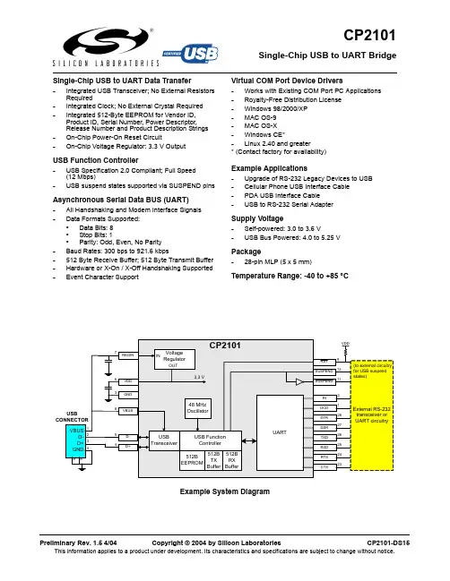
Single-Chip USB to UART BridgeCP2101Single-Chip USB to UART Data Transfer-Integrated USB Transceiver; No External Resistors Required-Integrated Clock; No External Crystal Required -Integrated 512-Byte EEPROM for Vendor ID, Product ID, Serial Number, Power Descriptor, Release Number and Product Description Strings -On-Chip Power-On Reset Circuit-On-Chip Voltage Regulator: 3.3 V OutputUSB Function Controller-USB Specification 2.0 Compliant; Full Speed (12 Mbps)-USB suspend states supported via SUSPEND pinsAsynchronous Serial Data BUS (UART)-All Handshaking and Modem Interface Signals -Data Formats Supported:•Data Bits: 8•Stop Bits: 1•Parity: Odd, Even, No Parity -Baud Rates: 300 bps to 921.6 kbps-512 Byte Receive Buffer; 512 Byte Transmit Buffer -Hardware or X-On / X-Off Handshaking Supported -Event Character SupportVirtual COM Port Device Drivers-Works with Existing COM Port PC Applications -Royalty-Free Distribution License -Windows 98/2000/XP -MAC OS-9-MAC OS-X -Windows CE*-Linux 2.40 and greater* (Contact factory for availability)Example Applications-Upgrade of RS-232 Legacy Devices to USB -Cellular Phone USB Interface Cable -PDA USB Interface Cable -USB to RS-232 Serial Adapter Supply Voltage-Self-powered: 3.0 to 3.6 V-USB Bus Powered: 4.0 to 5.25 V Package-28-pin MLP (5 x 5 mm)Temperature Range: -40 to +85 °CCP2101Table of Contents1.System Overview (4)2.Absolute Maximum Ratings (4)Table 2.1. Absolute Maximum Ratings (4)3.Global DC Electrical Characteristics (5)Table 3.1. Global DC Electrical Characteristics (5)Table 3.2. UART and Suspend I/O DC Electrical Characteristics (5)4.Pinout and Package Definitions (6)Table 4.1. Pin Definitions for the CP2101 (6)Figure 4.1. MLP-28 Pinout Diagram (Top View) (7)Figure 4.2. MLP-28 Package Drawing (8)Table 4.2. MLP-28 Package Dimensions (8)Figure 4.3. Typical MLP-28 Landing Diagram (9)Figure 4.4. Typical MLP-28 Solder Mask (10)B Function Controller and Transceiver (11)Figure 5.1. Typical Connection Diagram (11)6.Asynchronous Serial Data Bus (UART) Interface (12)Table 6.1. Data Formats and Baud Rates (12)7.Internal EEPROM (12)Table 7.1. Default USB Configuration Data (12)8.Virtual Com Port Device Drivers (13)9.Voltage Regulator (14)Table 9.1. Voltage Regulator Electrical Specifications (14)Figure 9.1. Configuration 1: USB Bus-Powered (14)Figure 9.2. Configuration 2: USB Self-Powered (15)Figure 9.3. Configuration 3: USB Self-Powered, Regulator Bypassed (15)1.System OverviewThe CP2101 is a highly-integrated USB-to-UART Bridge Controller providing a simple solution for updating RS-232 designs to USB using a minimum of components and PCB space. The CP2101 includes a USB 2.0 full-speed function controller, USB transceiver, oscillator, EEPROM and asynchronous serial data bus (UART) with full modem control signals in a compact 5 x 5 mm MLP-28 package. No other external USB components are required.The on-chip EEPROM may be used to customize the USB Vendor ID, Product ID, Product Description String, Power Descriptor, Device Release Number and Device Serial Number as desired for OEM applications. The EEPROM is programmed on-board via the USB allowing the programming step to be easily integrated into the product manufacturing and testing process.Royalty-free Virtual COM Port (VCP) device drivers provided by Silicon Laboratories allow a CP2101-based product to appear as a COM port to PC applications. The CP2101 UART interface implements all RS-232 signals, including control and handshaking signals, so existing system firmware does not need to be modified. In many existing RS-232 designs, all that is required to update the design from RS-232 to USB is to replace the RS-232 level-translator with the CP2101.An evaluation kit for the CP2101 (Part Number: CP2101EK) is available. It includes a CP2101-based USB-to-UART/RS-232 evaluation board, a complete set of VCP device drivers, USB and RS-232 cables, and full documentation. Contact a Silicon Labs’ sales representatives or go to to order the CP2101 Evaluation Kit.2.Absolute Maximum RatingsTable 2.1. Absolute Maximum RatingsParameter Conditions Min Typ Max Units Ambient temperature under bias–55—125°C Storage Temperature–65—150°C Voltage on any I/O Pin or RST with respect to–0.3— 5.8V GNDVoltage on V DD with respect to GND–0.3— 4.2V Maximum Total current through V DD and GND——500mA——100mA Maximum output current sunk by RST or anyI/O pinNote: stresses above those listed under “Absolute Maximum Ratings” may cause permanent damage to the device. This is a stress rating only and functional operation of the devices at those or any other condi-tions above those indicated in the operation listings of this specification is not implied. Exposure to maxi-mum rating conditions for extended periods may affect device reliability.CP21013.Global DC Electrical CharacteristicsTable 3.1. Global DC Electrical CharacteristicsV DD = 2.7 to 3.6 V, –40 to +85 °C unless otherwise specifiedParameter Conditions Min Typ Max Units Supply Voltage 3.0 3.3 3.6V Supply Current V DD = 3.3 V—25—mA Supply Current in Suspend V DD = 3.3 V—325—µA Specified Operating Temperature Range–40—+85°CTable 3.2. UART and Suspend I/O DC Electrical CharacteristicsV DD = 2.7 to 3.6 V, -40 to +85 °C unless otherwise specifiedParameters Conditions Min Typ Max UNITSOutput High Voltage I OH = -3mAI OH = -10µAI OH = -10mAVDD-0.7VDD-0.1VDD-0.8VOutput Low Voltage I OL = 8.5mAI OL = 10µAI OL = 25mA 1.00.60.1VInput High Voltage 2.0V Input Low Voltage0.8V Input Leakage Current2550µACP21014.Pinout and Package DefinitionsTable 4.1. Pin Definitions for the CP2101Name Pin #Type DescriptionV DD6Power InPowerOut3.0–3.6 V Power Supply Voltage Input.3.3 V Voltage Regulator Output. See Section 9.GND3GroundRST9 D I/O Device Reset. Open-drain output of internal POR or V DD monitor. An external source can initiate a system reset by driving this pin low for at least 15 µs.REGIN7Power In 5 V Regulator Input. This pin is the input to the on-chip voltage regu-lator.VBUS8 D In VBUS Sense Input. This pin should be connected to the VBUS signal of a USB network. A 5 V signal on this pin indicates a USB network connection.D+4 D I/O USB D+D–5 D I/O USB D–TXD26 D Out Asynchronous data output (UART Transmit) RXD25 D In Asynchronous data input (UART Receive) CTS23* D In Clear To Send control input (active low)RTS24* D Out Ready to Send control output (active low)DSR27* D in Data Set Ready control input (active low)DTR28* D Out Data Terminal Ready control output (active low) DCD1* D In Data Carrier Detect control input (active low)RI2* D In Ring Indicator control input (active low)SUSPEND12* D Out This pin is driven high when the CP2101 enters the USB suspend state.SUSPEND11* D Out This pin is driven low when the CP2101 enters the USB suspend state.NC10, 13–22These pins should be left unconnected or tied to V DD. *Note: Pins can be left unconnected when not used.CP2101Figure 4.1. MLP-28 Pinout Diagram (Top View)CP2101Figure 4.2. MLP-28 Package DrawingTable 0.1. MLP-28 Package DimensionsMM MIN TYP MAX A 0.800.90 1.00A100.020.05A200.65 1.00A3—0.25—b 0.180.230.30D — 5.00—D2 2.90 3.15 3.35E — 5.00—E2 2.90 3.15 3.35e —0.5—L 0.450.550.65N —28—ND —7—NE —7—R 0.09——AA —0.435—BB —0.435—CC —0.18—DD—0.18—CP2101Figure 4.3. Typical MLP-28 Landing DiagramCP2101Figure 4.4. Typical MLP-28 Solder Mask11Rev. 1.5B Function Controller and TransceiverThe Universal Serial Bus function controller in the CP2101 is a USB 2.0 compliant full-speed device with integrated transceiver and on-chip matching and pull-up resistors. The USB function controller manages all data transfers between the USB and the UART as well as command requests generated by the USB host controller and commands for controlling the function of the UART.The USB Suspend and Resume signals are supported for power management of both the CP2101 device as well as external circuitry. The CP2101 will enter Suspend mode when Suspend signaling is detected on the bus. On entering Suspend mode, the CP2101 asserts the SUSPEND and SUSPEND signals. SUSPEND and SUSPEND are also asserted after a CP2101 reset until device configuration during USB Enumeration is completeThe CP2101 exits the Suspend mode when any of the following occur: (1) Resume signaling is detected or generated, (2) a USB Reset signal is detected, or (3) a device reset occurs. On exit of Suspend mode, the SUSPEND and SUSPEND signals are de-asserted.Both SUSPEND and SUSPEND temporarily float high during a CP2101 reset. If this behavior is undesirable, a strong pulldown (10 kΩ) can be used to ensure SUSPEND remains low during reset. See Figure 5.1 for other recommended options.Figure 5.1. Typical Connection DiagramRev. 1.5126.Asynchronous Serial Data Bus (UART) InterfaceThe CP2101 UART interface consists of the TX (transmit) and RX (receive) data signals as well as the RTS, CTS, DSR, DTR, DCD and RI control signals. The UART supports RTS/CTS, DSR/DTR and X-On/X-Off handshaking.The UART is programmable to support a variety of data formats and baud rates. The data format and baud rate programmed into the UART is set during COM port configuration on the PC. The data formats and baud rates available are listed in Table 6.1.7.Internal EEPROMThe CP2101 includes an internal EEPROM that may be used to customize the USB Vendor ID, Product ID, Product Description String, Power Descriptor, Device Release Number and Device Serial Number as desired for OEM applications. Customization of the USB configuration data is optional. If the EEPROM is not programmed with OEM data, the default configuration data shown in Table 7.1 is used. However, a unique serial number is required for OEM applications in which it is possible for multiple CP2101-based devices to be connected to the same PC.The internal EEPROM is programmed via the USB. This allows the OEM's USB configuration data and serial number to be written to the CP2101 on-board during the manufacturing and testing process. A stand-alone utility for programming the internal EEPROM is available from Silicon Laboratories. A library of routines provided in the form of a Windows ® DLL is also available. This library can be used to integrate the EEPROM programming step into custom software used by the OEM to streamline testing and serial number management during manufacturing. The EEPROM has a typical endurance of 100,000 write cycles with a data retention of 100 years.Table 6.1. Data Formats and Baud RatesData Bits 8Stop Bits 1Parity Type None, Even, OddBaud Rates300, 600, 1200, 1800, 2400, 4800, 7200, 9600, 14400, 19200, 28800, 38400, 56000, 57600, 115200, 128000, 230400, 460800, 921600Table 7.1. Default USB Configuration DataName Value Vendor ID 10C4h Product IDEA60h Power Descriptor (Attributes)80hPower Descriptor (Max. Power)32h Release Number 0100hSerial Number0001 (63 characters maximum)Product Description String“CP2101 USB to UART Bridge Controller” (126 characters maximum)13Rev. 1.58.Virtual Com Port Device DriversThe CP2101 Virtual COM Port (VCP) device drivers allow a CP2101-based device to appear to the PC's application software as an additional COM port (in addition to any existing hardware COM ports). Application software running on the PC accesses the CP2101-based device as it would access a standard hardware COM port. However, actual data transfer between the PC and the CP2101 device is performed over the USB. Therefore, existing COM port applications may be used to transfer data via the USB to the CP2101-based device without modifying the application. Contact Silicon Laboratories for the latest list of supported operating systems.Note:The Silicon Laboratories VCP device drivers are required for device operation and are only distributed as part of the CP2101 Evaluation Kit (Part Number: CP2101EK). Contact any of Silicon Lab’s sales representatives or go to to order the CP2101 Evaluation Kit. The CP2101 drivers and programming utilities are subject to change without notice. Subscription to the website "Auto Email Alert" system for automatic notification of updates and the use of the "Product Update Registration" service is recommended.Rev. 1.5149.Voltage RegulatorThe CP2101 includes an on-chip 5-to-3 V voltage regulator. This allows the CP2101 to be configured as either a USB bus-powered device or a USB self-powered device. These configurations are shown in Figure 9.1 and Figure 9.2. When enabled, the 3 V voltage regulator output appears on the V DD pin and can be used to power external 3V devices. See Table 9.1 for the voltage regulator electrical characteristics.Alternatively, if 3 V power is supplied to the V DD pin, the CP2101 can function as a USB self-powered device with the voltage regulator disabled. For this configuration, it is recommended that the REGIN input be tied to the 3 V net to disable the voltage regulator. This configuration is shown in Figure 9.3.The USB max power and power attributes descriptor must match the device power usage and configuration. See application note “AN144: CP2101 Customization Guide” for information on how to customize USB descriptors for the CP2101.Note:It is recommended that additional decoupling capacitance (e.g., 0.1 µF in parallel with 1.0 µF) be provided on the REGIN input.Figure 9.1. Configuration 1: USB Bus-PoweredTable 9.1. Voltage Regulator Electrical Specifications–40 to +85 °C unless otherwise specifiedParameterConditionsMin Typ Max Units Input Voltage Range 4.0— 5.25V Output VoltageOutput Current = 1 to 100 mA*3.0 3.3 3.6V VBUS Detection Input Threshold 1.0 1.84.0V Bias Current—90TBDµA* The maximum regulator supply current is 100 mA.15Rev. 1.5Figure 9.2. Configuration 2: USB Self-PoweredFigure 9.3. Configuration 3: USB Self-Powered, Regulator BypassedRev. 1.516Document Change ListRevision 1.4 to Revision 1.5Updated Example System Diagram on page 1.Updated Table 3.1, “Global DC Electrical Characteristics,” on page 5.Added Table 3.2, “UART and Suspend I/O DC Electrical Characteristics,” on page 5 Added Table note to Table 4.1, “Pin Definitions for the CP2101,” on page 6 Added Figure 5.1. , "Typical Connection Diagram" on page 11Removed asterisk from the “Linux 2.40 and greater” bullet on page 117Rev. 1.5NotesRev. 1.518Contact InformationSilicon Laboratories Inc.4635 Boston Lane Austin, TX 78735Tel: 1+(512) 416-8500 Fax: 1+(512) 416-9669 Toll Free: 1+(877) 444-3032Email:********************** Internet: Silicon Laboratories and Silicon Labs are trademarks of Silicon Laboratories Inc.Other products or brandnames mentioned herein are trademarks or registered trademarks of their respective holdersThe information in this document is believed to be accurate in all respects at the time of publication but is subject to change without notice. Silicon Laboratories assumes no responsibility for errors and omissions, and disclaims responsibility for any consequences resulting from the use of information included herein. Additionally, Silicon Laboratories assumes no responsibility for the function-ing of undescribed features or parameters. Silicon Laboratories reserves the right to make changes without further notice. Silicon Laboratories makes no warranty, representation or guarantee regarding the suitability of its products for any particular purpose, nor does Silicon Laboratories assume any liability arising out of the application or use of any product or circuit, and specifically disclaims any and all liability, including without limitation consequential or incidental damages. Silicon Laboratories products are not designed, intended, or authorized for use in applications intended to support or sustain life, or for any other application in which the failure of the Silicon Laboratories product could create a situation where personal injury or death may occur. Should Buyer purchase or use Silicon Laboratories products for any such unintended or unauthorized application, Buyer shall indemnify and hold Silicon Laboratories harmless against all claims and damages.。
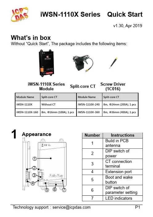
iWSN-1110X Series Quick Startv1.30, Apr 2019W hat’s in boxW ithout “Quick St art”, The package includes the following items:iWSN-1110X Series Module Split-core CTScrew Driver(1C016)Module Name Split-core CT Module Name Split-core CTiWSN-1110X Without CTiWSN-1110X-240 8m, Φ24mm (200A), 1 pcs iWSN-1110X-1608m, Φ16mm (100A), 1 pcsiWSN-1110X-3608m, Φ36mm (400A), 1 pcs1 AppearanceNumberInstructions1 Build in PCB antenna2DIP switch of power3 CT connection terminal4 Extension port5 Boot and wake button6 DIP switch of parameter setting 7LED indicators○1 ○3 ○4 ○6 ○7○5 ○22 Pin and buttonSwitch InstructionsPWRON Power onOFF Power offPin Name Instructions4 N/AReserved, empty orshorted3 N/A2 CT Split-core CT pin,nodirectionality,supportmeasuring andcharging function1 CTExtension bus InstructionsExt_Bus Empty or connect extension moduleButton Instructions Wake Manual wake upBoot After pressing for 1~3 seconds, the LED light will be on for 1 second and then off. This meanboot complete.3 Communication parameterName InstructionsF2Reserved F1TX Duty ( RF transmitduty )■:ON □:OFF PeriodPin5 6 1 sec □□10 sec ■□30 sec □■60 sec ■■RF Ch ( RF Channel) ■:ON□:OFF ChPinChPin1 2 3 4 1 2 3 40 □□□□8 □□□■1 ■□□□9 ■□□■2 □■□□ A □■□■3 ■■□□ B ■■□■4 □□■□ C □□■■5 ■□■□ D ■□■■6 □■■□ E □■■■7 ■■■□ F ■■■■Name Instructions PA Factory OnlyGID (Group ID) ■:ON □:OFF GroupPin6 70 □□1 ■□2 □■3 ■■Node ID■:ON □:OFF NodePinNodePin1 2 3 4 5 1 2 3 4 50 □□□□□16 □□□□■1 ■□□□□17 ■□□□■2 □■□□□18 □■□□■3 ■■□□□19 ■■□□■4 □□■□□20 □□■□■5 ■□■□□21 ■□■□■6 □■■□□22 □■■□■7 ■■■□□23 ■■■□■8 □□□■□24 □□□■■9 ■□□■□25 ■□□■■10 □■□■□26 □■□■■11 ■■□■□27 ■■□■■12 □□■■□28 □□■■■13 ■□■■□29 ■□■■■14 □■■■□30 □■■■■15 ■■■■□31 ■■■■■4 LED indicatorsThe module provides one LED indicator. The table below will show the LED status.5Boot stepsA. Please confirm the CT is locked into the module, and “Ext_Bus ” isconnected an extension module by audio line. (If there is no extensionmodule, the “Ext_Bus ” don ’t be connected.)B. Adjusting DIP switch and set the parameter of communication, and switch“PWR ” to OFF. And then switch “PWR ” to ON after press “Wake ” and “Boot ” buttons for 5 seconds.C. When power on, if “STA ” will light on for 1 second and off, this mean bootcomplete. If “STA ” do not be lighted, please press “Boot ” for 1~3 seconds, and confirm “STA ” will light on for 1 second and off. Finally, press “Wake ” once, confirm “STA ” blink once to complete the boot.D. Connect the CT to the cable to be measured. The buckle has nodirectionality, but after the buckle, you must confirm that the opening is completely closed.Before the CT be buckledAfter the CT be buckledConfirm the opening is completely closed○A ○B ○D ○CNote:1. if you need to remove the terminal lines, always detach the CT before removing the CT terminal lines. Otherwise the CT may develop open-circuit secondary voltages which may be hazardous to personnel or damaging to the CT or equipment connected in the secondary circuit.2.The external CT’s are fragile, please handle with care.3. The current input of the iWSN-1120X series only supports the factory-attached CT.4.To install CT’s correctly, please ensure the CT lines sequences is r ight before clip the CT’s onto the power cable of the monitoring equipment.5.Please select the appropriate size CT for different size monitoring equipment cables: power line diame ter <Φ24 using 200A CT, Φ36 using 400A CT.6.The maximum current value cannot exceed the CT rating.6 Application exampleThe module will measure the current data and transmit automatically to iWSN-2200 by wireless. The user can use computer to read the data in iWSN-2200 by Modbus RTU protocol.WarningICP DAS assumes no liability for any damage resulting from the use of this product. ICP DAS reserves the right to change this manual at any time without notice. The information furnished by ICP DAS is believed to be accurate and reliable. However, no responsibility is assumed by ICP DAS for its use, not for any infringements of patents or other rights of third parties resulting from its use.Limitation of WarrantyThis warranty does not apply to defects resulting from unauthorized modification, misuse, or use for reason other than electrical power monitoring. The supplied meter is not a user-serviceable product. Product Warranty & Customer SupportICP DAS warrants all products free from defects in material and workmanship for a period of one year from the date of shipping. During the warranty period, we will, at our position, either repair or replace any product that proves to be defective. To report any defect, please contact us. Please have the model, serial number and a detailed problem description available when you call. If the problem concerns a particular reading, please have all meter readings available. When returning any merchandise to ICP DAS, a return SN. Is required.。

FUJITSU Image ScannersSP-1120, SP-1125, SP-1130, SP-1425Future-proof. Simplified scanning opens doors for professional document capture Resourceful. Purpose built with impressive software suite for efficiency gains Reliable. Intuitively and dependably converts physical documents to digital formatConvenient. Simple and easy to use design, ideal for desktop placementRaise your productivityEasily evolve from your physical to electronic documents with the SP Series. Create one single reference source for all your data by merging paper documents with your digitally born documents. Gain the business advantages of working with more convenient, flexible and secure digital images using simple push button routines, the SP Series feature a simple operation panel with two buttons (Scan / Stop and Power).Store, retrieve and manage your documents more productively, efficiently and cost effectively than paper records allow. At the same time activelyembrace compliance risk avoidance concerns and increase your customer’s satisfaction.Cost effective high performance Achieve more in less time. Remove your backlog of documents and transform mixed batches of different thicknesses and sizes including plastic cards into high quality images. The SP Series has been especially designed to provide a simple but efficient paper to digital document scanning platform for all types of businesses looking to adopt a more systematic approach to regular document capture.Automatic size recognition and blank page removal simplifies scanning operations and pre scan sorting thereby helping to save theinconvenience of fine tuning the document for the OCR process. Fujitsu scanners are renowned for their highly reliable paper handling capabilities and these help remove image capture disruptions to reduce document management overheads.Desktop convenienceWith the ADF models measuring less than an A4 size sheet of paper the compact designtakes up minimal space on a busy desktop. The small footprint means these devices are always available and within reach for uninterrupted performance. Trade a small desktop space to reclaim a much larger space taken up by paper records. Whether it’ll be sets of loose sheets of documents scanned through all SP Series models’ automatic document feeders (ADFs) or bound materials that need to be scannedwith the SP-1425 flatbed module, the SP Seriesconveniently supports the user in regularly digitizing all office documents.PaperStream Capture Lite PaperStream Capture Lite is a powerful application used to scan documents with the SP Seriesscanner models. It is extremely easy-to-use and provides an interface similar to a mobile application. This allows users with little scanning experience to use the scanner almost instantly. PaperStream Capture Lite is based on the “One Click Capture” concept, which promotes reducing the number of times to touch the screen. It is effective in the prevention of operational errors as well as streamlining repeated operations. PaperStream Capture Lite presents itself as an essential capture tool for feeding TIF, BMP or JPEG files into defined capture routines by simply selecting a pictogram presented on screen.Bundled with business enhancing functionalityTurn lifeless business records into searchable, secure yet dynamic documents that can be fed into digital archives. The bundled version of ABBYY FineReader Sprint creates searchable and editable files from your paper documents allowing you to retrieve information more efficiently at a future date (the OCR processing can handle 190 languages). Call this application directly from within your PaperStream Capture Lite profile and searchable PDF and PDF/A files are just one click away.Presto PageManager offers further manifold possibilities for the enhancement, conversion and organisation of your personally used files.Faster throughput when it is neededThe SP Series models through their 50-sheet automatic document feeder (ADF) can process single or double sided pages at the same time. The SP-1120 can scan 20 A4 single sided pages per minute (ppm) or 40 images per minute (ipm), the SP-1125 and SP-1425 scan speeds are 25 ppm / 50 ipm and the SP-1130 scan speeds are 30 ppm / 60 ipm./scannersPFU (EMEA) Limited Hayes Park CentralHayes End Road, Hayes Middlesex UB4 8FE United KingdomPFU (EMEA) Limited Frankfurter Ring 21180807 Munich GermanyPFU (EMEA) Limited Viale Monza, 25920126 Milano (MI)ItalyPFU (EMEA) LimitedCamino Cerro de los Gamos, 128224 Pozuelo de Alarcón Madrid SpainTel: +44 (0)20 8573 4444Tel: +49 (0)89 32378 0Tel: +39 02 26294 1All indications are non-binding. Technical data is subject to change without prior notification.Bundled softwarePaperStream IP – high quality image enhancementPaperStream IP is the scanner driver for the SP Series. In addition to being fully compliant with the industry standard TWAIN and ISIS interface, PaperStream IP incorporates as standard, highly sophisticated image processing that automatically applies features such as noise removal, background pattern removal and character augmentation to produce exceptionally clear, high quality images that are suitable for direct import into the users’ workflow.PaperStream IP has an intuitive, easy to use interface that can be switched between Administrator or User mode to simplify the scanning process and reduce user error.Additionally PaperStream IP also introduces a new Assisted Scanning mode, which allows the user to visually select the best quality image from a range of images of the page, rather than needing to manually fine tune the scanning parameters one by one.Developed to be the best in class scanner driver。
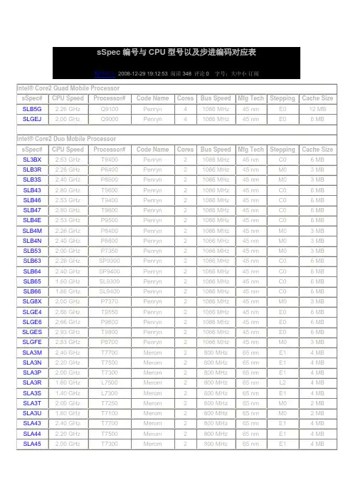
sSpec编号与CPU型号以及步进编码对应表数码电子2008-12-29 19:12:53 阅读348 评论0 字号:大中小订阅Intel® Core2 Quad Mobile ProcessorsSpec#CPU Speed Processor#Code Name Core s Bus Speed Mfg Tech Stepping Cache Size SLB5G 2.26 GHz Q9100Penryn41066 MHz45 nm E012 MB SLGEJ 2.00 GHz Q9000Penryn41066 MHz45 nm E0 6 MBIntel® Core2 Duo Mobile ProcessorsSpec#CPU Speed Processor#Code Name Core s Bus Speed Mfg Tech Stepping Cache Size SL3BX 2.53 GHz T9400Penryn21066 MHz45 nm C0 6 MB SLB3R 2.26 GHz P8400Penryn21066 MHz45 nm M0 3 MB SLB3S 2.40 GHz P8600Penryn21066 MHz45 nm M0 3 MB SLB43 2.80 GHz T9600Penryn21066 MHz45 nm C0 6 MB SLB46 2.53 GHz T9400Penryn21066 MHz45 nm C0 6 MB SLB47 2.80 GHz T9600Penryn21066 MHz45 nm C0 6 MB SLB4E 2.53 GHz P9500Penryn21066 MHz45 nm C0 6 MB SLB4M 2.26 GHz P8400Penryn21066 MHz45 nm M0 3 MB SLB4N 2.40 GHz P8600Penryn21066 MHz45 nm M0 3 MB SLB53 2.00 GHz P7350Penryn21066 MHz45 nm M0 3 MB SLB63 2.26 GHz SP9300Penryn21066 MHz45 nm C0 6 MB SLB64 2.40 GHz SP9400Penryn21066 MHz45 nm C0 6 MB SLB65 1.60 GHz SL9300Penryn21066 MHz45 nm C0 6 MB SLB66 1.86 GHz SL9400Penryn21066 MHz45 nm C0 6 MB SLG8X 2.00 GHz P7370Penryn21066 MHz45 nm M0 3 MB SLGE4 2.66 GHz T9550Penryn21066 MHz45 nm E0 6 MB SLGE6 2.66 GHz P9600Penryn21066 MHz45 nm E0 6 MB SLGES 2.93 GHz T9800Penryn21066 MHz45 nm E0 6 MB SLGFE 2.53 GHz P8700Penryn21066 MHz45 nm M0 3 MB SLA3M 2.40 GHz T7700Merom2800 MHz65 nm E1 4 MB SLA3N 2.20 GHz T7500Merom2800 MHz65 nm E1 4 MB SLA3P 2.00 GHz T7300Merom2800 MHz65 nm E1 4 MB SLA3R 1.60 GHz L7500Merom2800 MHz65 nm L2 4 MB SLA3S 1.40 GHz L7300Merom2800 MHz65 nm E1 4 MB SLA3T 2.00 GHz T7250Merom2800 MHz65 nm M0 2 MB SLA3U 1.80 GHz T7100Merom2800 MHz65 nm M0 2 MB SLA43 2.40 GHz T7700Merom2800 MHz65 nm E1 4 MB SLA44 2.20 GHz T7500Merom2800 MHz65 nm E1 4 MB SLA45 2.00 GHz T7300Merom2800 MHz65 nm E1 4 MBSLA4A 1.80 GHz T7100Merom2800 MHz65 nm M0 2 MB SLA75 2.60 GHz T7800Merom2800 MHz65 nm G0 4 MB SLADL 2.40 GHz T7700Merom2800 MHz65 nm G0 4 MB SLADM 2.20 GHz T7500Merom2800 MHz65 nm G0 4 MB SLAEB 1.60 GHz T5470Merom2800 MHz65 nm M0 2 MB SLAF6 2.60 GHz T7800Merom2800 MHz65 nm G0 4 MB SLAF7 2.40 GHz T7700Merom2800 MHz65 nm G0 4 MB SLAF8 2.20 GHz T7500Merom2800 MHz65 nm G0 4 MB SLAP9 2.10 GHz T8100Penryn2800 MHz45 nm M0 3 MB SLAPA 2.40 GHz T8300Penryn2800 MHz45 nm M0 3 MB SLAPR 2.40 GHz T8300Penryn2800 MHz45 nm M0 3 MB SLAPS 2.10 GHz T8100Penryn2800 MHz45 nm M0 3 MB SLAPT 2.10 GHz T8100Penryn2800 MHz45 nm M0 3 MB SLAPU 2.40 GHz T8300Penryn2800 MHz45 nm C0 3 MB SLAPV 2.50 GHz T9300Penryn2800 MHz45 nm C0 6 MB SLAPW 2.60 GHz T9500Penryn2800 MHz45 nm C0 6 MB SLAQG 2.50 GHz T9300Penryn2800 MHz45 nm C0 6 MB SLAQH 2.60 GHz T9500Penryn2800 MHz45 nm C0 6 MB SLAUU 2.10 GHz T8100Penryn2800 MHz45 nm C0 3 MB SLAVJ 2.10 GHz T8100Penryn2800 MHz45 nm M0 3 MB SLAX G 2.10 GHz T8100Penryn2800 MHz45 nm M0 3 MB SLAYP 2.10 GHz T8100Penryn2800 MHz45 nm M0 3 MB SLAYQ 2.40 GHz T8300Penryn2800 MHz45 nm M0 3 MB SLAYX 2.60 GHz T9500Penryn2800 MHz45 nm C0 6 MB SLAYY 2.50 GHz T9300Penryn2800 MHz45 nm C0 6 MB SLAYZ 2.10 GHz T8100Penryn2800 MHz45 nm M0 3 MB SLAZA 2.60 GHz T9500Penryn2800 MHz45 nm C0 6 MB SLAZB 2.50 GHz T9300Penryn2800 MHz45 nm C0 6 MB SLAZC 2.40 GHz T8300Penryn2800 MHz45 nm M0 3 MB SLAZD 2.10 GHz T8100Penryn2800 MHz45 nm M0 3 MB SLB5Q 1.20 GHz SU9300Penryn2800 MHz45 nm M0 3 MB SLB6E 2.00 GHz T5800Merom2800 MHz65 nm M0 2 MB SLGHN 1.40 GHz SU9400Penryn2800 MHz45 nm M0 3 MB SL9SD 2.33 GHz T7600Merom2667 MHz65 nm B2 4 MB SL9SE 2.16 GHz T7400Merom2667 MHz65 nm B2 4 MB SL9SF 2.00 GHz T7200Merom2667 MHz65 nm B2 4 MB SL9SG 1.83 GHz T5600Merom2667 MHz65 nm B2 2 MB SL9SH 1.66 GHz T5500Merom2667 MHz65 nm B2 2 MB SL9SJ 2.33 GHz T7600Merom2667 MHz65 nm B2 4 MBSL9SL 2.00 GHz T7200Merom2667 MHz65 nm B2 4 MBSL9SM 1.50 GHz L7400Merom2667 MHz65 nm B2 4 MBSL9SN 1.33 GHz L7200Merom2667 MHz65 nm B2 4 MBSL9SP 1.83 GHz T5600Merom2667 MHz65 nm B2 2 MBSL9SQ 1.66 GHz T5500Merom2667 MHz65 nm B2 2 MB SL9U3 1.83 GHz T5600Merom2667 MHz65 nm L2 2 MB SL9U4 1.66 GHz T5500Merom2667 MHz65 nm L2 2 MB SL9U7 1.83 GHz T5600Merom2667 MHz65 nm L2 2 MB SL9U8 1.66 GHz T5500Merom2667 MHz65 nm L2 2 MB SLA4D 2.00 GHz T5750Merom2667 MHz65 nm M0 2 MB SLA4E 1.83 GHz T5550Merom2667 MHz65 nm M0 2 MB SLA4F 1.66 GHz T5450Merom2667 MHz65 nm M0 2 MB SLA9S 1.50 GHz T5250Merom2667 MHz65 nm M0 2 MBSL9VP 1.60 GHz T5200Merom2533 MHz65 nm B2 2 MBSL9WE 1.73 GHz T5300Merom2533 MHz65 nm L2 2 MB SLA2U 1.20 GHz U7600Merom2533 MHz65 nm L2 2 MB SLA2V 1.06 GHz U7500Merom2533 MHz65 nm L2 2 MB SLV3W 1.33 GHz U7600Merom2533 MHz65 nm M0 2 MB SLV3X 1.20 GHz U7500Merom2533 MHz65 nm M0 2 MBIntel® Pentium® Dual-Core Mobile ProcessorsSpec# CPU Speed Processor#Code Name Core s Bus Speed Mfg Tech Stepping Cache Size SLAVG 2.00 GHz T3200Merom2667 MHz65 nm M0 1 MB SLA4H 1.86 GHz T2390Merom2533 MHz65 nm M0 1 MB SLA4J 1.73 GHz T2370Merom2533 MHz65 nm M0 1 MB SLA4K 1.60 GHz T2330Merom2533 MHz65 nm M0 1 MB SLAEC 1.46 GHz T2310Merom2533 MHz65 nm M0 1 MB SL9VZ 1.86 GHz T2130Merom2533 MHz65 nm D0 1 MBSL9VY 1.73 GHz T2080Merom2533 MHz65 nm D0 1 MBSL9VX 1.60 GHz T2060Merom2533 MHz65 nm D0 1 MBIntel® Celeron® Mobile ProcessorsSpec# CPU Speed Processor#Code Name Core s Bus Speed Mfg Tech Stepping Cache Size SLGAS 1.20 GHz723N/A2800 MHz45 nm M0 1 MB SLB6J 1.66 GHz T1600Merom2667 MHz65 nm M0 1 MB SLB6H 1.83 GHz T1700Merom2667 MHz65 nm M0 1 MB SLB6M 2.00 GHz575Conroe L1667 MHz65 nm M0 1 MB SLB6L 2.16 GHz585Conroe L1667 MHz65 nm M0 1 MBSL8X W 1.06 GHz423Conroe L1533 MHz65 nm C0 1 MBSL9L8 1.20 GHz443Conroe L1533 MHz65 nm D0 1 MBSL8W2 1.46 GHz410Conroe L1533 MHz65 nm C0 1 MBSL9WN 1.60 GHz520Conroe L1533 MHz65 nm A1 1 MB SL8VZ 1.60 GHz420Conroe L1533 MHz N/A C0 1 MBSL9WT 1.60 GHz520Conroe L1533 MHz65 nm B2 1 MB SL92F 1.73 GHz430Conroe L1533 MHz65 nm C0 1 MB SLA2G 1.73 GHz530Conroe L1533 MHz65 nm A1 1 MBSL9KV 1.73 GHz430Conroe L1533 MHz65 nm D0 1 MBSL9VA 1.73 GHz530Conroe L1533 MHz65 nm A1 1 MB SLA2F 1.86 GHz540Conroe L1533 MHz65 nm A1 1 MBSL9KW 1.86 GHz440Conroe L1533 MHz65 nm D0 1 MB SLA2E 2.00 GHz550Conroe L1533 MHz65 nm A1 1 MBSL9KX 2.00 GHz450Conroe L1533 MHz65 nm D0 1 MB SLA2D 2.13 GHz560Conroe L1533 MHz65 nm A1 1 MBIntel® Atom ProcessorsSpec# CPU Speed Processor#Code Name Core s Bus Speed Mfg Tech Stepping Cache Size SLB2H 1.33 GHz Z520Silverthorne1533 MHz45 nm C0512 KB SLG9Y 1.60 GHz330N/A2533 MHz45 nm C0 1 MB SLB73 1.60 GHz N270Silverthorne1533 MHz45 nm C0512 KB SLB6Z 1.60 GHz230Silverthorne1533 MHz45 nm C0512 KB SLB6P 1.60 GHz Z530Silverthorne1533 MHz45 nm C0512 KB SLB2M 1.86 GHz Z540Silverthorne1533 MHz45 nm C0512 KB SLB6Q800 MHz Z500Silverthorne1400 MHz45 nm C0512 KB SLB2C 1.10 GHz Z510Silverthorne1400 MHz45 nm C0512 KB。


Suse Linux 11 双机集群配置文档一安装前准备1.两台装有suse 11 sp1操作系统的服务器,每台服务器有两块网卡。
2.Suse 11 sp1系统安装碟或者ISO文件。
3.suse 11 sp1 HA 安装碟或者iso文件SLE-11-SP1-HA-x86_64-GM-Media1.iso二安装Heartbeat通过yast2工具添加heartbeat,选择软件—附加产品如图1:图1附加产品安装添加HA应用url勾选“高可用性”安装三Heartbeat配置下面以浙江移动流量服务器双机热备为例,讲述heartbeat的配置。
1. 网卡设置主服务器:bond0 10.70.238.157/26 bond0:0 10.7.8.1备服务器:bond0 10.70.238.158/26 bond0:0 10.7.8.2浮动IP:10.70.238.159/26(之后将对其进行配置)因浙江移动要求主机双线路,所以服务器上两网卡做了bond,两台服务器的bond0:0口用直通线连接作为心跳线2.主机系统配置(1) 在两台服务器上修改/etc/hosts文件,修改内容如下:10.70.238.157 pc-zjdamglk01.site pc-zjdamglk0110.70.238.158 pc-zjdamglk02.site pc-zjdamglk0210.7.8.1 pc-zjdamglk01.site pc-zjdamglk0110.7.8.2 pc-zjdamglk02.site pc-zjdamglk023. 开启同步服务在主服务器上开启同步服务,配置如下:1、启动YaST 并选择杂项> 群集或在命令行中运行yast2 cluster 启动初始群集配置对话框。
2、在通讯通道类别中,配置用于群集节点间通讯的通道。
此信息会写入/etc/ais/openais.conf 配置文件。
通信通道用10.7.8.0网段,组播地址,端口不变。
The BlackArmor® NAS 110 server is a network attached storage solution designed to provide centralized storage,data backup and media streaming for up to 10 PCs. Help protect important data with automatic full-systembackup, SafetyDrill+™ bare metal recovery software and powerful hardware-based encryption.Highlights• D esigned to provide centralized storage and data backup for up to 10 PCs.• Protect network connected PCs with incremental and full-system, automatic backup.*• Secure files with powerful hardware-based encryption.• Functions as an FTP server, enabling remote file access.• Stream media to DLNA® compliant devices and computers running iTunes® software.• O neTouch® backup button duplicates files from storage devices such as digital cameras and USB drivesconnected to the front USB port.• Includes a reliable Seagate® hard drive.• Connect external drives, share a printer or utilize an uninterrupted power supply with the two USB 2.0 ports.• Event email notification.• 3-year limited warranty.Copyright © 2009 Seagate Technology LLC. All rights reserved. Seagate, Seagate Technology and the Wave logo are registered trademarks of Seagate Technology LLC in the United States and/or other countries.BlackArmor, SafetyDrill+, and Global Access are either trademarks or a registered trademarks of Seagate Technology LLC or one of its affiliated companies in the United States and/or other countries. All other trademarksor registered trademarks are the property of their respective owners. When referring to hard drive capacity, one gigabyte, or GB, equals one billion bytes and one terabyte, or TB, equals one trillion bytes. Your computer’soperating system may use a different standard of measurement and report a lower capacity. In addition, some of the listed capacity is used for formatting and other functions, and thus will not be available for data storage.Seagate reserves the right to change, without notice, product offerings or specifications. The export or re-export of hardware or software containing encryption may be regulated by the U.S. Department of Commerce, Bureauof Industry and Security (for more information go to ) DS1695.1-0909Visit for more information about these and other Seagate retail products.Perfect for when you need to:• S tore and access files from acentral, secure location.• A ccess and manage filesremotely.• S tream media to DLNAcompliant devices orcomputers running iTunes®software.• A utomatically perform full-system backups on networkconnect PCs.• S ecure files with hardware-based encryption.• S hare a USB printer withnetwork connected PCs andMacs.Interface 10/100/1000 Ethernet, USB 2.0Capacities1TB, 2TBProduct Dimensions Horiz x Vert x Depth - 2.40”x 6.90” x 5.80” (61.00mm x 176.00mm x 147.00mm)Weight: 2.71lbs (1.22kg)Retail Packaging Specs Box dimensions: Horiz x Vert x Depth – 9.29” x 9.02” x 3.66” (235.97mm x 229.11mm x 92.96mm)Box weight: 3.64lbs (1.65kg)Master carton dimensions: Horiz x Vert x Depth – 11.50” x 10.08” x 9.41” (292.1mm x 256.03mm x 239.01mm)Master carton weight: 11.98lbs (5.43kg)Master carton quantity: 3Master cartons per pallet: 64Pallet dimensions: Horiz x Vert x Depth – 48.00” x 48.43” x 40” (1,219.2mm x 1,230.12mm x 1,016mm)Pallet weight: 812.00lbs (368.32kg)Pallet layers: 4Technical Specifications ConnectivityNetwork ProtocolsNetwork AuthenticationFile Sharing ProtocolsVolume ManagementDisk ManagementBackup ManagementEvent ManagementMedia StreamingDownload ServerRemote Access• 1 internal SATA II port• 2 USB 2.0 host portsCIFS NFS, HTTP, HTTPS, FTP, Bonjour®Microsoft Windows® Server Active DirectoryCIFS, NFS, HTTPS, FTP• Share management• Volume level encryption• Multi-volume management• SMART status monitor• L ocal backup(USB device to NAS, NAS to USB device)• Network NAS to NAS backupEvent email notification• iTunes® server• DLNA® compliant digital media serverDownloader (HTTP and FTP)Seagate Global Access™ service• 1 RJ45 Ethernet port (Gigabit)• Share/folder-level access control list (ACL) support• Quotas setting• Drive standby mode• C lient system backup, Bare Metal Restore(full-system recovery) over network• OneTouch® USB storage device backupSoftware Requirements PC On Network• Pentium® III, 500MHz equivalent processor or higher• Microsoft Windows® XP or Microsoft Vista® OS• I nternet Explorer® 6.0 browser or later, or Firefox™ 2.Xbrowser or later (for management interface and web access)• 256MB RAMMac On Network• Mac OS® X 10.4.11 OS or later• Apple® Safari® 3.1 browser or laterSystem Requirements• Local area network (LAN)• Internet connection (for system updates and web access)• W ired or wireless router with an available 10/100/1000Ethernet port• USB printer or USB disk drive (optional)Inside the Box • BlackArmor NAS 110 storage server• 2M – RJ45 cable• AC power cord• Quick Start Guide• CD-ROM with– BlackArmor® Discovery Software for Windows® OS– BlackArmor® Discovery Software for Mac® OS– B lackArmor® Backup Software for Windows OS(5 licenses*)– Online registration link– Warranty information card*Additional licenses available for purchase at Connectivity• O ne Ethernet port for localnetwork connection, web-based management and remoteaccess.• T wo USB 2.0 ports for externaldrives, printers and uninterruptedpower supplies (UPS).• One internal SATA II port.* Includes data backup software licenses for 5 PCs. Additional licenses available for purchase at .Full-system ProtectionSoftware plays an important role in helping to protect your valuable data and with BlackArmor, you can expect nothing less than the best. To help protect all the files on your PC, our software package provides automatic, incremental and full-system backup. In the event of PC hardware failure, you can utilize the SafetyDrill+™ bare metal restore feature to recover your entire system, including the operating system, programs and settings. Furthermore, the included software also allows you to secure your files with powerful 256-bit encryption.You’re in ControlIn addition to the included backup software, the web-based management interface and BlackArmor ® Discovery tool software are also straightforward to use. The BlackArmor Discovery tool software allows you to get up and running quickly by displaying all of the BlackArmor NAS products connected to your network. From the discovery tool, with a single click, you can view or map shared volumes to your computer, access the web-based user interface or back up the PC you are working from. The BlackArmor NAS 110 storage server can also be managed remotely with DDNS, which can be configured from the web-based management interface.The BlackArmor NAS 110 storage server can function as an FTP server, allowing remote access to files. Using the web-based management interface, you can designate user access manually or integrate with Microsoft ® Active Directory.Moreover, the BlackArmor NAS 110 storage server canstream media files to DLNA ® compliant devices or computers running iTunes ® software, allowing you to centralize media and display content simultaneously on multiple devices.Designed to provide centralized storage and data backup.ExpansionThe one rear-mounted USB 2.0 port allows you to connect an external USB hard drive for additional storage, easily share a USB printer with your network connected computers or connect an uninterrupted power supply (UPS) to safeguard from power failure.OneTouch ® BackupThe OneTouch backup button duplicates files from USB storage devices such as drives and digital cameras connected to the front-mounted USB port.。
H400-450HDS SERIESTECHNICAL GUIDE2H400-450HDS DIMENSIONSCircled dimensions correspond to the line numbers on the tabulated chart inside the Technical Guide. Dimensions are in inches (millimeters).4-214-354-14-44-194-54-24-71-81-94-324-204-14-313H400-450HDS SPECIFICATIONSCERTIFICATION: Hyster lift trucks meet the design and construction requirements of B56.1-1969, per OSHA Section 1910.178(a)(2), and also comply with the B56.1 revision in effect at time of manufacture. Certification of compliance with the applicable ANSI standards appears on the lift truck. Performance specifications are for a truck equipped as described under Standard Equipment on this technical guide. Performance specifications are affected by the condition of the vehicle and how it is equipped, as well as by the nature, condition of the operating area, proper service andmaintenance of the vehicle. If these specifications are critical, the proposed application should be discussed with your dealer.G E N E R A LDescriptionUnitsEnglish Metric English Metric 1-1Manufacturer HYSTER HYSTER HYSTER HYSTER 1-2Model designation H400HDS H400HDS H450HDS H450HDS 1-5Rated load capacity lbs kg 40,00018,14445,00020,4121-6Load center in mm 36914369141-8Load distance in mm 421,069421,0691-9Wheelbasein mm 1383,5001383,500W E I G H T S2-1Total truck weight without load lbs kg 61,96328,10666,41630,1262-2a Axle loading with loadfront lbs kg 93,83542,563102,12746,3242-2b rear lbs kg 8,1283,6879,2904,2142-3a Axle loading without load front lbs kg 31,31714,20532,32214,6612-3b rearlbskg 30,64613,90134,09415,465W H E E L S3-1Tire type Pneumatic Pneumatic 3-2Tire sizefront 14.00 x 24 14.00 x 24 3-3rear14.00 x 24 14.00 x 24 D I M E N S I O N S4-1Mast tilt, forward / back degrees 10 / 1210 / 124-2Height of mast lowered in mm 1634,1421674,2304-3Freelift (Top of Fork) w/o LBR in mm 00004-4Lift height (Top of Fork)in mm 1834,6501834,6504-5Height of mast extended w/o LBR in mm 2536,4172566,5054-7Height to top of operator compartment in mm 1333,3721333,3724-19Overall length in mm 3127,9273117,9104-20Length to load face in mm 2165,4872155,4704-21Overall width over drive tires in mm 1152,9231152,9234-22a Forkthickness in mm 3.94100 3.941004-22b width in mm 7.92009.82504-22c lengthin mm 962,440962,4404-24Carriage width in mm 1052,6721152,9404-25a Fork spread, min (in-in)in mm 411,048431,0974-25b Fork spread, max (out-out)in mm 942,3931072,7124-31Ground clearance, under mast with load in mm 12307112784-32Ground clearance, center of wheelbasein mm 153********-33Aisle width (Right angle stack) add load length + clearance in mm 365927136492464-35Outside turning radius in mm 194492819449288-7Hydraulic tank capacity gal L 54203542038-8Fuel tank capacity gal L 8030480304P E R F O R M A N C E (T I E R 4)PERFORMANCEWITH TIER 4 FINAL CUMMINS QSB 6.7L ENGINE5-1a Travel speedwith load mph km/h 162516255-1b without load mph km/h 162516255-2a Lifting speed with load ft/min m/s 590.30 490.25 5-2b without load ft/min m/s 650.33 550.28 5-3a Lowering speed with load ft/min m/s 980.50 980.50 5-3b without loadft/min m/s 980.50 980.50 5-6Drawbar Pull – MaxlbskN43,60019443,5001935-7Gradeability – no load / rated load – 1 mph (1.6 km/h)%38 / 3334 / 32P E R F O R M A N C E (T I E R 3)PERFORMANCEWITH TIER 3 CUMMINS QSB 6.7L ENGINE5-1a Travel speedwith load mph km/h 162516255-1b without load mph km/h 162516255-2a Lifting speed with load ft/min m/s 590.30 490.25 5-2b without load ft/min m/s 650.33 550.28 5-3a Lowering speed with load ft/min m/s 980.50 980.50 5-3b without loadft/min m/s 980.50 980.50 5-6Drawbar Pull – MaxlbskN45,60020345,5002035-7Gradeability – no load / rated load – 1 mph (1.6 km/h)%38 / 3334 / 324H400-450HDS SPECIFICATIONSCERTIFICATION: Hyster lift trucks meet the design and construction requirements of B56.1-1969, per OSHA Section 1910.178(a)(2), and also comply with the B56.1 revision in effect at time of manufacture. Certification of compliance with the applicable ANSI standards appears on the lift truck. Performance specifications are for a truck equipped as described under Standard Equipment on this technical guide. Performance specifications are affected by the condition of the vehicle and how it is equipped, as well as by the nature, condition of the operating area, proper service andmaintenance of the vehicle. If these specifications are critical, the proposed application should be discussed with your dealer.G E N E R A LDescriptionUnitsEnglish Metric English Metric 1-1Manufacturer HYSTER HYSTER HYSTER HYSTER 1-2Model designation H400HD H400HD H450HD H450HD 1-5Rated load capacity lbs kg 40,00018,14445,00020,4121-6Load center in mm 36914369141-8Load distance in mm 431,086431,0861-9Wheelbasein mm 1483,7501483,750W E I G H T S2-1Total truck weight without load lbs kg 59,39926,94363,83328,9542-2a Axle loading with loadfront lbs kg 91,61541,556100,26845,4812-2b rear lbs kg 7,7853,5318,5653,8852-3a Axle loading without load front lbs kg 30,59813,87932,11714,5682-3b rearlbskg 28,80113,06431,71814,387W H E E L S3-1Tire type Pneumatic Pneumatic 3-2Tire sizefront 14.00 x 24 14.00 x 24 3-3rear14.00 x 24 14.00 x 24 D I M E N S I O N S4-1Mast tilt, forward / back degrees 10 / 1210 / 124-2Height of mast lowered in mm 1634,1421674,2304-3Freelift (Top of Fork) w/o LBR in mm 00004-4Lift height (Top of Fork)in mm 1834,6501834,6504-5Height of mast extended w/o LBR in mm 2536,4172566,5054-7Height to top of operator compartment in mm 1333,3721333,3724-19Overall length in mm 3228,1773218,1604-20Length to load face in mm 2265,7372255,7204-21Overall width over drive tires in mm 1152,9231152,9234-22a Forkthickness in mm 3.94100 3.941004-22b width in mm 7.92009.82504-22c lengthin mm 962,440962,4404-24Carriage width in mm 1052,6721152,9404-25a Fork spread, min (in-in)in mm 411,048431,0974-25b Fork spread, max (out-out)in mm 942,3931072,7124-31Ground clearance, under mast with load in mm 12307112784-32Ground clearance, center of wheelbasein mm 153********-33Aisle width (Right angle stack) add load length + clearance in mm 3789,6013789,6014-35Outside turning radius in mm 2075,2582075,2588-7Hydraulic tank capacity gal L 54203542038-8Fuel tank capacity gal L 8030480304P E R F O R M A N C E (T I E R 4)PERFORMANCEWITH TIER 4 FINAL CUMMINS QSB 6.7L ENGINE5-1a Travel speedwith load mph km/h 162516255-1b without load mph km/h 162516255-2a Lifting speed with load ft/min m/s 890.45 750.38 5-2b without load ft/min m/s 980.50 830.42 5-3a Lowering speed with load ft/min m/s 980.50 980.50 5-3b without loadft/min m/s 980.50 980.50 5-6Drawbar Pull – MaxlbskN48,40021543,5001945-7Gradeability – no load / rated load – 1 mph (1.6 km/h)%39 / 3435 / 33P E R F O R M A N C E (T I E R 3)PERFORMANCEWITH TIER 3 CUMMINS QSB 6.7L ENGINE5-1a Travel speedwith load mph km/h 162516255-1b without load mph km/h 162516255-2a Lifting speed with load ft/min m/s 890.45 750.38 5-2b without load ft/min m/s 980.50 830.42 5-3a Lowering speed with load ft/min m/s 980.50 980.50 5-3b without loadft/min m/s 980.50 980.50 5-6Drawbar Pull – MaxlbskN45,70020345,6002035-7Gradeability – no load / rated load – 1 mph (1.6 km/h)%39 / 3435 / 335H400-450HDS SPECIFICATIONSH400HD/S MAST DIMENSIONS4-4 Lift Height (Top of Fork)4-2 Mast Lowered Ht.4-3 Freelift (Top of Fork)4-5 Overall Extended Ht.inmminmminmminmm2-STAGE ONLY 1473750145369200217551718346501634142002536417212540017945170028271672446200194491700314796726367002035167003338467275700020953173458767H450HD/S MAST DIMENSIONS4-4 Lift Height (Top of Fork)4-2 Mast Lowered Ht.4-3 Freelift (Top of Fork)4-5 Overall Extended Ht.inmminmminmminmm2-STAGE ONLY1473750149378000221560518346501674230002566505212540018146050028672552446200197500500317805526367002075255003378555275700021454053498855POWERTRAINSUNITS TIER 4 FINALTIER 31-3Power typeDiesel Diesel 7-1Engine Manufacturer / model Cummins QSB 6.7LCummins QSB 6.7L7-2a Engine power output - Rated hp kW 2201642201647-2b Engine power output - Peak hpkW 2301682301687-3Governed speedrpm 2,0002,0007-4Number of cylinders / displacement # / l 6 / 6.76 / 6.77-5Engine torque - Max lb-ft N-m 7009497009497-5a Turbocharger Type Water-Cooled Variable GeometryWater-Cooled Variable Geometry7-9Alternator outputAmps1201207-10a Drive Axle Manufacturer / Model AxleTech AxleTech 8-0Transmission Manufacturer / model ZF WG 211 5-speed ZF WG 211 5-speed 8-1Drive control / Transmission: Number of speeds forward/reverse Powershift 5F x 3R Powershift 5F x 3R 8-6Battery voltage, rated capacity V / CCA 2 x 12 / 900 2 x 12 / 9005-10Service brake Oil immersed (wet) disc Oil immersed (wet) disc 5-11Park brake Dry Disc on Drive Axle Dry Disc on Drive Axle 10-4DEF Tank Capacitygall 1038N/AN/ARated capacities are for trucks equipped with:• 2-stage (lower mast) to 147” (3750 mm) maximum fork height • 105” (2672 mm) carriage width (H400HD/S)• 115” (2940 mm) carriage width (H450HD/S)• 96” (2440 mm) long forksContact your dealer for other capacity information.Model H400HDS: 40,000 lbs. at 36” (18,144 kg at 914mm) load centerModel H450HDS: 45,000 lbs. at 36” (20,412 kg at 914mm) load center Model H400HD: 40,000 lbs. at 36” (18,144 kg at 914mm) load center Model H450HD: 45,000 lbs. at 36” (20,412 kg at 914mm) load center Conversion Factor: 1.0” = 25.4 mm 1 lb = 0.45 kg2000025000 300003500040000450005000024 283236404448525660646872R A T E D L O A D (l b s )LOAD C ENTER (in) RATED L OAD v s L OAD C ENTER | D FSSFP H OOK T YPE | U .S. C USTOMARY H400HD, H 400HDS H450HD, H 450HDSRATED LOAD VS. LOAD CENTER | DFSSFP HOOK TYPE | U.S. CUSTOMARYLOAD CENTER (in)R A T E D L O A D (l b s )H400HD, H400HDS H450HD, H450HDS2000025000300003500040000 450005000024 28 32 36404448525660646872R A T E D L O A D (l b s )LOAD C ENTER (in) RATED L OAD v s L OAD C ENTER | D FSSFP P IN T YPE | U .S. C USTOMARY H400HD, H 400HDS H450HD, H 450HDSRATED LOAD VS. LOAD CENTER | DFSSFP PIN TYPE | U.S. CUSTOMARYR A T E D L O A D (l b s )LOAD CENTER (in)H400HD, H400HDS H450HD, H450HDSRATED CAPACITIES6STANDARD FEATURES AND OPTIONSMASTSMasts with nested channels provide excellent visibility of the attachment and load. Mast channels, rollers, stub shafts and chain anchors are reinforced to provide good torsional rigidity.CARRIAGESTwo dual function sideshift fork positioner (DFSSFP) carriage options are available: hook type and pin type.FORKSTwo kinds of forks are offered:1. PIN TYPE - STANDARD PROFILE available in: – H400HD/S 96” long x 3.9” x 7.8” (2440mm x 100mm x 200mm) 84” long x 3.9” x 7.8” (2135mm x 100mm x 200mm)– H450HD/S 96” long x 3.9” x 9.8” (2440mm x 100mm x 250mm) 84” long x 3.9” x 7.8” (2135mm x 100mm x 200mm)2. HOOK TYPE (FOR USE WITH DFSSFP) available in:– H400HD/S 96” long x3.9” x 7.8” (2440mm x 100mm x 200mm)– H450HD/S 96” long x 3.9” x 9.8” (2440mm x 100mm x 250mm)ENGINE – TIER 4 FINALCummins QSB 6.7L 6-cylinder diesel engine delivers 230 hp and 700 lb-ft of maximum torque. EPA Tier 4 Final engine features cooled exhaust gas recirculation (EGR) technology with selective catalytic reduction (SCR); water-cooled variable geometry turbocharger with an integrated diesel exhaust fluid (DEF) delivery system. Innovative selectable ECO performance modes offer excellent fuel economy and maximum productivity. Requires ultra-low sulphur diesel fuel and low ash oil. Also includes:• 120 amp alternator• Viscous, on-demand cooling fan that saves fuel and reduces noise• Overhead exhaust with diesel oxidation catalyst and a diluter to reduce exhaust temperatures • Automatic throttle-up• Heavy duty spinner type Sy-Klone pre-cleaner center, stacked for ease of serviceENGINE – TIER 3Cummins QSB 6.7L 6-cylinder diesel engine delivers 230 peak hp and 700 lb-ft of maximum torque. EPA Tier 3 engine features an integrated muffler. Can be used in markets where ultra-low sulphur diesel fuel and low ash oil is not available. Also includes:• 120 amp alternator • Automatic throttle-upTRANSMISSION• ZF WG 211 5-speed powershift transmission providessmooth shifting, precise inching and quick acceleration • 5 forward and 3 reverse gears • Electronically controlled inching• Cushioned clutch lock-up provides smooth shifting and dampens drive line shift shocks • Simple push button calibration• Transmission lock-out prevents high-speed directional changes• Transmission and engine powertrain protection for excessive engine coolant temperature, low engine oil pressure, and excessive engine inlet air temperatures.ELECTRICAL SYSTEM• Sealed Deutsch connectors.• CANbus system for easy diagnostics of engine, transmission and hydraulics.• 24V electrical system with 900 CCA batteries.HYDRAULIC SYSTEMHyster on-demand load-sensing hydraulic system introduces an efficient way to meet hydraulic load demands:• Based on Variable Displacement Pump (VDP) technology.• Pump is only active when oil is needed.• Less heat is produced, helping oil and filters last longer. Hoses, seals, and components also wear less and last longer.• Engine runs quieter and at lower speeds, extending life of major components.• Up to 10% fuel savings from on-demand hydraulics.• Leak free O-ring face seal (ORFS) fittings standard throughout the truck.• Capable of more oil displacement even at low engine speeds.7STANDARD FEATURES AND OPTIONSSTEERING SYSTEM• The steer axle is characterized by transverse mounted double acting cylinders, 2 non-adjustable tie rods, 2 spindles, tapered roller bearings and 2 wheel hubs.• Designed for high loads and long life, the one piece axle frame carries the axle loads and provides mounting for the spindles and cylinder.• Axle spindles are supported by tapered roller wheel bearings and sealed to prevent loss of grease. This ensures that oil bearings are always lubricated and enhances overall durability of the axle spindles.• Eight high-strength bolts secure the steer cylinder providing large wheel angles and excellentmaneuverability. Excessive external force on the frame is avoided using this design.• No steering linkage adjustments are required.Lubricating fittings on spindle and tie rod pins are the only regular maintenance points.• Load sensed steering provides low steering effort and good performance at all engine speeds.DRIVE AXLERugged drive axle features full-floating design. Wheel hubs rotate on large tapered roller bearings.BRAKESThe oil-cooled wet disc brake system greatly extends brake system life.OPERATOR AREA• Ergonomically designed hydraulic controls and direction control lever are within easy reach.• Three steps and hand grips provide easy access to operator compartment.• Angled floor plate and pedals are positioned for operator comfort.• Telescopic, tilt steer column.• Supportive mechanical full-suspension seat adjusts 8 inches (200 mm) for operator comfort.• Several air suspension seat options are available.• Steel overhead guard frame provides excellent high stacking visibility.• Operator Presence System (OPS) with complete hydraulic lock out requires the operator to be in thenormal operating position before any travel or movement of the mast, tilt, carriage, and attachment can beinitiated. Travel or movement of the mast, tilt, carriage, and attachment is locked out when the operator leaves the seat for more than 2-3 seconds.• Optional light groups aid visibility in low-lighted areas. Light kits featuring innovative High-performance LED and halogen technology are available.• Optional ComforCab II features:– tinted, curved glass – circulation fan– heater and defroster– electric wiper and windshield washer (front, rear, top)– intermittent front wiper – door retainer – 3-speed fan– 12-volt auxiliary power source – dome light– additional options to enhance comfort and productivityHyster Company P .O. Box 7006Greenville, North Carolina 27835-7006Part No. H400-450HDS/TG 10/2017 Litho in U.S.A.Trucks may be shown with optional equipment. © 2017 Hyster Company. All rights reserved.Hyster, , and STRONG PARTNERS. TOUGH TRUCKS. and MONOTROL are registered trademarks in the United States and certain other jurisdictions. Hyster products are subject to change without notice.Visit us online at or call us at 1-800-HYSTER-1.STANDARD EQUIPMENT• 147” (3750mm) max fork ht 2-stage mast with 141” overall lowered ht (H400HD/S)• 147” (3750mm) max fork ht 2-stage mast with 147” overall lowered ht (H450HD/S)• 105” (2672mm) wide pin type dual function sideshift fork positioner (H400HD/S)• 115” (2940mm) wide pin type dual function sideshift fork positioner (H450HD/S)• 96” long x 3.9” x 7.8” (2440mm x 100mm x 200mm) forks (H400HD/S)• 96” long x 3.9” x 9.8” (2440mm x 100mm x 250mm) forks (H450HD/S)• Cummins QSB 6.7L Tier 4 Final engine with cooled EGR and SCR • Wet disc brakes• Sy-Klone spinner type heavy duty air intake pre-cleaner • Premium ZF WG 211 5-speed autoshift transmission • AxleTech heavy duty planetary drive axles• Powertrain protection system for engine and transmission; high temp. or low oil pressure• On-demand load-sensing hydraulic system featuring VDP technology • 5-function hydraulic control valve with 3 levers, 2 switches• CANbus electrical control system for engine, transmission and hydraulics • 14.00 x 24 - 28PR bias ply treaded load pneumatic drive and steer tires • Directional control lever with direction change interlock system • Mast tilt: 10° forward / 12° back • Lockable battery disconnect switch • 120 amp alternator•Open operator compartment with integral overhead guard, includes:– seatside mini-lever hydraulic control – multifunction display panel– telescoping & tilting steering column – floor mat– isolated mounting for low noise and vibration – 24-12V DC converter– full-suspension vinyl seat with integrated, adjustable armrest & seat belt – exterior wide angle mirrors, mounted to handrails • Operator restraint system • Operator presence system • Electronic horn - 105 dB(A)• Visible alarm / amber strobe light • Audible backup alarm • 24V electrical system• Tilting operator compartment for service access - manual operation• Light Kit – FRONT: 2 halogen mast mounted lights; 2 halogen lights on front fender; REAR: 2 halogen cab mounted lights; 2 LED stop / tail / back-up lights • Steering wheel with spinner knob • Steer wheel nut protection • Non-locking fuel cap• Literature package: operator’s manual, service manual, parts manual •12 months / 2,000 hours manufacturer’s warrantyOPTIONAL EQUIPMENT• Cummins QSB 6.7L Tier 3 engine rated at 220 hp (230 hp peak) with variable geometry turbocharger*• Various 2-stage lift masts available • Various mast tilt options • Mast tilt indicator• Hook type dual function sideshift fork positioner carriages• Various hydraulic valve control groups • Multifunction joystick control• MONOTROL ® pedal direction control with direction change interlock system• Radial and pneumatic shaped solid tires • Enclosed cab options:– air conditioning – trainer seat– 24-12V DC converter, 2nd outlet– front (single blade), top & rear wipers – recirculation fan– accessory mounting post• Rear camera systems with cab mounted display• Front and rear mud flaps • Multiple seat options• 2- or 3-point high-visibility seat belt• Powered tilting operator compartment for service access• Various HP LED and halogen light kits available• Automatic greasing system • Fuel strainer in fuel filler neck• Centralized greasing provision for mast chain sheaves• Battery jump start connector (NATO plug)• Lifting eyes• Seatbelt interlock for engine start • Engine block heater (110v or 230V)• Traction speed limiter• Empty seat engine shutdown • Belly pansOther options available through Special Products EngineeringDevelopment (SPED). Contact Hyster Company for details.* Available in non-regulated markets as standard powertrain.Available as an option in EPA regulated markets in limited quantities.。
DataOrdering dataProduct type descriptionTESZ1110/S Article number (order number)101029152EAN (European Article Number)4030661449111eCl@ss number, Version 9.027-27-06-09CertificationsCertificates DGUVcULusCCC EACGeneral dataProduct nameTESZ StandardsIEC/EN 60947-5-1 BG-GS-ET-15 Enclosure material Plastic, glass-fibre reinforced thermoplastic, self-extinguishing Material of the contacts, electrical SilverMaterial of the hingeAluminium Gross weight 280 gGeneral data - Featuresmounting hingeYes Number of safety contacts 3TESZ1110/SDouble-insulatedThermoplastic enclosure111,5 mm x 92 mm x 36 mm 2 cable entries M 20 x 1.5Good resistance to oil and petroleum spiritSimple fitting, especially on 40mm profilesSafety appraisalStandards ISO 13849-1Mission Time20 Year(s)Safety appraisal - Safety outputsB10d Normally-closed contact2,000,000 Operations(NC)B10d Normally open contact (NO)1,000,000 OperationsMechanical dataMechanical life, minimum1,000,000 OperationsPositive break angle14 °Positive break force, minimum 1 NMechanical data - Connection techniqueTerminal Connector Screw connectionCable section, minimum0.5 mm²Cable section, maximum 1 mm²Note (Cable section)All indications about the cable section are including the conductor ferrules. Mechanical data - DimensionsLength x Width x Height Suitable for mounting to profile systems: 40 mmHeight of sensor92 mmLength of sensor36 mmWidth of sensor111.5 mmAmbient conditionsProtection class IP65Ambient temperature, minimum-25 °CAmbient temperature, maximum+65 °CAmbient conditions - Insulation valueRated impulse withstand voltage 2.5 kVElectrical dataThermal test current 2.5 AUtilisation category AC-15230 VACUtilisation category AC-15 2 AUtilisation category DC-1324 VDCUtilisation category DC-13 1 ASwitching element Opener (NC) Switching principle Creep circuit element Switching frequency120 /hNotesNote (General)The opening angle has been set to 4° in factory.The additional hinge including mounting accessories is also available separately, part number TES/SOrdering codeProduct type description:TESZ(1)(2)(3)(4)/(5)(6)/(7)(1)without Material of the hinge AluminiumX Material of the hinge Stainless steel(2)R mechanische Wiederanlaufsperre(3)10 1 NC contact102 1 NC contacts / 1 NO contact110 2 NC contact1102 2 NC contacts / 1 NO contacts1110 3 NC contact(4)without Screw connectionST1Connector bottom (M12, 8 pole)ST2Connector top (M12, 8 pole)(5)without with additional hingeS without additional hinge(6)30Suitable for mounting to profile systems 30 mm 35Suitable for mounting to profile systems 35 mmwithout Suitable for mounting to profile systems 40 mm45Suitable for mounting to profile systems 45 mm(7)without Switching angle NC contact at 4 degrees5°Switching angle NC contact at 5 degrees8°Switching angle NC contact at 8 degreesPicturesProduct picture (catalogue individual photo)ID: ktez-f06| 598,2 kB | .jpg | 352.778 x 314.678 mm - 1000 x 892Pixel - 72 dpi| 47,3 kB | .png | 74.083 x 65.969 mm - 210 x 187Pixel - 72 dpi| 70,6 kB | .jpg | 27.093 x 24.13 mm - 320 x 285 Pixel -300 dpiDimensional drawing basic componentID: 5tez-g03| 6,1 kB | .png | 74.083 x 61.031 mm - 210 x 173 Pixel- 72 dpi| 194,2 kB | .jpg | 352.778 x 291.042 mm - 1000 x 825Pixel - 72 dpi| 43,9 kB | .cdr || 43,4 kB | .jpg | 112.889 x 93.133 mm - 320 x 264Pixel - 72 dpiSwitch travel diagramID: ktes-s05| 16,8 kB | .jpg | 112.889 x 38.453 mm - 320 x 109Pixel - 72 dpi| 19,3 kB | .cdr || 1,7 kB | .png | 74.083 x 25.047 mm - 210 x 71 Pixel -72 dpiDiagramID: ktes-k05| 23,7 kB | .jpg | 112.889 x 48.683 mm - 320 x 138Pixel - 72 dpi| 18,4 kB | .cdr |K.A. Schmersal GmbH & Co. KG, Möddinghofe 3, D-42279 WuppertalThe details and data referred to have been carefully checked. Images may diverge from original. Further technical data can be found in the manual. Technical amendments and errors possible.Generated on 08.07.2020 17:25:59。
up .w hd 1. 如何阅读本章所有 LPC111x 系列中的 SPI 模块均相同。
第二个 SPI 模块, SPI1,只存在于LQFP48和 PLCC44封装上,在 HVQFN33封装上则没有。
注释:两个 SPI 模块都包含全部的 SSP 特征集,所有相关寄存器都使用 SSP 前缀命名。
2. 特性? 兼容 Motorola SPI 、 4线 TI SSI 和美国国家半导体公司的 Microwire 总线。
? 同步串行通信。
? 支持主机和从机操作。
? 收发均有 8帧 FIFO 。
?每帧有 4-16位数据。
3. 基本描述SPI/SSP是一个同步串行端口 (SSP控制器,可控制 SPI 、 4线 SSI 和 Microwire 总线。
它可以与总线上的多个主机和从机相互作用。
在数据传输过程中,总线上只能有一个主机与一个从机进行通信。
原则上数据传输是全双工的, 4~16位帧的数据由主机发送到从机或由从机发送到主机。
但实际上,大多数情况下只有一个方向上的数据流包含有意义的数据。
LPC111x 系列处理器有两个 SPI/同步串行端口控制器。
u d u UM10398Semiconductors LPC1100开发,尽在第 11章 :LPC111x 带有 SSP 的 SPI0/1 4. 引脚描述表 161622. SPI 引脚描述SCK0/1I/OSCK CLK SK 串行时钟。
SCK/CLK/SK是用来同步数据传输的时钟信号。
它由主机驱动,从机接收。
当使用 SPI 接口时,时钟可编程为高电平有效或低电平有效,否则总是高电平有效。
SCK 仅在数据传输过程中切换。
在其它时间里, SPI/SSP接口保持无效状态或不驱动它(使其处于高阻态。
SSEL0/1I/OSSEL FS CS 帧同步 /从机选择。
当 SPI/SSP接口是总线主机时,它在串行数据启动前驱动该信号为有效状态。
在数据发送出去之后又将该信号恢复为无效状态。
详解服务器性能测试基准体系20世纪90年代,TPC(Transaction Processing Performance Council,事务处理性能委员会)成立,Benchmark(基准测试)随之走上历史舞台,企业采购服务器时,除主观三围指标之外,理性的光芒开始闪耀。
TPC单位为tpmC,对系统在线事务处理能力进行评价,表示每分钟内系统处理新订单的个数,主要模拟企业的MIS、ERP等系统来考验服务器联机业务处理能力。
SPEC(标准性能评估机构)是另一个全球性的、权威的第三方应用性能测试组织,它旨在确立、修改和认证一系列服务器应用性能评估的标准。
目前主要包括:•针对CPU性能的SPECCPU2000、SPEC CPU2006•针对Web服务器的SPECWeb2005•针对高性能计算的SPEC HPC2002与SPEC MPI2006•针对Java应用的SPECjAppServer2004与SPEC JBB2005,以及对图形、网络、邮件服务器的测试指标。
此外,还有常见的四大应用中的基准测试和专用基准测试:•1)高性能计算(HPC):Linpack…•2)在线事务处理(OLTP):TPC-C…•3)Web服务:SPEC Web2005、TPC-W•4)Java应用服务器:SPECjbb2005专用基准测试:•1) Oracle基准测试•2) SAP基准测试等SPEC基准测试介绍SPEC是一个全球性的、权威的第三方应用性能测试组织,它旨在确立、修改以及认定一系列服务器应用性能评估的标准。
由于它体现了软、硬件平台的性能和成本指标,被金融、电信、证券等关键行业用户作为选择IT系统一项权威的选型指标。
SPEC组织始建于1988年,当时是由几个计算机设备供应商为了开发和支持大范围的计算机系统的性能测试程序而成立的,今天这个组织有60多家知名公司加入和支持,如:Intel、AMD、IBM、HP等公司。
SPEC提供用于评估邮件服务器、WEB服务器、文件服务器、超级计算机和计算机集群、CPU、专业图形应用等方面的评估软件。
Kramer Electronics, Ltd.USER MANUALModel:VM-1110xlBalanced Audio DistributorContentsContents1Introduction 1 2Getting Started 1 2.1Quick Start 2 3Overview 3 4Your VM-1110xl Balanced Audio Distributor 3 5Installing the VM-1110xl in a Rack 6 6Connecting Your VM-1110xl 6 6.1Connecting a 1:10 Mono DA 7 6.2Connecting a 2x1:5 Mono DA 8 6.3Connecting a 1:5 Stereo DA 9 7Technical Specifications 10 FiguresFigure 1: VM-1110xl Balanced Audio Distributor 4 Figure 2: Connecting the VM-1110xl as a 1:10 Mono DA 7 Figure 3: Connecting the VM-1110xl as a 2x1:5 Mono DA 8 Figure 4: Connecting the VM-1110xl as a 1:5 Stereo DA 9 TablesTable 1: VM-1110xl Balanced Audio Distributor Features 5 Table 2: VM-1110xl Balanced Audio Distributor Technical Specifications 10Introduction1 IntroductionWelcome to Kramer Electronics! Since 1981, Kramer Electronics has been providing a world of unique, creative, and affordable solutions to the vastrange of problems that confront the video, audio, presentation, andbroadcasting professional on a daily basis. In recent years, we haveredesigned and upgraded most of our line, making the best even better!Our 1,000-plus different models now appear in 11 groups1 that are clearlydefined by function.Thank you for purchasing your Kramer VM-1110xl Balanced AudioDistributor.This product is ideal for the following typical applications:Audio duplication and production studios, delivering undiminished quality duplicatesRecording studiosBroadcast studios for on-line signal distributionEach package includes the following items:VM-1110xl Balanced Audio DistributorPower cord2This user manual32 Getting StartedWe recommend that you:Unpack the equipment carefully and save the original box and packaging materials for possible future shipmentReview the contents of this user manualUse Kramer high-performance high-resolution cables41 GROUP 1: Distribution Amplifiers; GROUP 2: Switchers and Matrix Switchers; GROUP 3: Control Systems; GROUP 4: Format/Standards Converters; GROUP 5: Range Extenders and Repeaters; GROUP 6: Specialty AV Products; GROUP 7: Scan Converters and Scalers; GROUP 8: Cables and Connectors; GROUP 9: Room Connectivity; GROUP 10: Accessories and Rack Adapters; GROUP 11: Sierra Products2 We recommend that you use only the power cord supplied with this device3 Download up-to-date Kramer user manuals from our Web site at Getting Started2.1 Quick StartThis quick start chart summarizes the basic setup and operation steps.Overview3 OverviewThe VM-1110xl is a high performance balanced audio DA (distributionamplifier) using XLR connectors. It can be configured as a mono (1:10 or 2x1:5) DA or as a stereo (1:5) DA.The VM-1110xl features:Front panel output level trimmer controlsActive Bi-FET amplifying circuitry that ensures hum-free, full-bandwidth operationA high-power discrete buffering system providing excellentperformanceTo achieve the best performance:Use only good quality connection cables1 to avoid interference, deterioration in signal quality due to poor matching, and elevatednoise levels (often associated with low quality cables).Avoid interference from neighboring electrical appliances that may adversely influence signal quality and position your KramerVM-1110xl away from moisture, excessive sunlight and dust4 Your VM-1110xl Balanced Audio DistributorFigure 1 and Table 1 define the VM-1110xl.Your VM-1110xl Balanced Audio Distributor4Figure 1: VM-1110xl Balanced Audio DistributorKRAMER: SIMPLE CREATIVE TECHNOLOGYYour VM-1110xl Balanced Audio DistributorTable 1: VM-1110xl Balanced Audio Distributor Features # Feature Function1 Power LED Lights when the unit is powered on2 1:10 / 2x1:5 Button Pushing in selects 2x1:51, releasing selects 1:1023 Level B Trimmer Adjusts3 the output signal level for OUTPUT B4 Level A Trimmer Adjusts3 the output signal level for OUTPUT A5 INPUT A XLR Female Connector Connects to the source A6 INPUT B XLR Female Connector Connects to the source B7 OUT A XLR Male Connector Connects to the acceptor A (from 1 to 5)8 OUT B XLR Male Connector Connects to the acceptor B (from 1 to 5)9 Power Connector with Fuse AC connector enabling power supply to the unit10 ON/OFF Switch Illuminated switch for powering the unit1 Splits inputs A and B to outputs 1A-5A and 1B-5B, respectively2 Splits input A to all 10 outputsInstalling the VM-1110xl in a Rack5 Installing the VM-1110xl in a RackThis section describes how to install the VM-1110xl in a rack.Before Installing in a rack How to Rack MountBefore installing in a rack, be sure that the environment is within the recommended range:Operating temperature range +5 to +45 C (41 to 113 F) Operating humidity range 10 to 90% RHL, non-condensing Storage temperature range -20 to +70 C (-4 to 158 F) Storage humidity range 5 to 95% RHL, non-condensingCAUTION!!When installing on a 19" rack, avoid hazards by taking care that:1. It is located within the recommended environmentalconditions, as the operating ambient temperature of a closed or multi unit rack assembly may exceed theroom ambient temperature.2. Once rack mounted, enough air will still flow aroundthe machine.3. The machine is placed straight in the correcthorizontal position.4. You do not overload the circuit(s). When connectingthe machine to the supply circuit, overloading thecircuits might have a detrimental effect on overcurrent protection and supply wiring. Refer to the appropriate nameplate ratings for information. For example, forfuse replacement, see the value printed on theproduct label.5. The machine is earthed (grounded) in a reliable wayand is connected only to an electricity socket withgrounding. Pay particular attention to situations where electricity is supplied indirectly (when the power cordis not plugged directly into the socket in the wall), forexample, when using an extension cable or a powerstrip, and that you use only the power cord that issupplied with the machine. To rack-mount a machine:1. Attach both ear brackets to themachine. To do so, remove thescrews from each side of themachine (3 on each side), andreplace those screws through theear brackets.2. Place the ears of the machineagainst the rack rails, and insert theproper screws (not provided)through each of the four holes in the rack ears.Note that:In some models, the front panel may feature built-in rack earsDetachable rack ears can beremoved for desktop useAlways mount the machine in the rack before you attach any cablesor connect the machine to thepowerIf you are using a Kramer rack adapter kit (for a machine that is not 19"), see the Rack Adapters usermanual for installation instructions(you can download it at:)6 Connecting Your VM-1110xlYou can connect your VM-1110xl Balanced Audio Distributor in one of three ways:1:10 mono DA, see section 6.12x1:5 mono DA, see section 6.21:5 stereo DA, see section 6.3To connect1 the VM-1110xl as a 1:10 mono DA, as the example in Figure 2 illustrates, do the following:1. Connect one mono audio source (for example, a mono audio player) toINPUT A on the rear panel.2. Connect up to 10 audio acceptors2 to the OUT connectors on the rear panel.3. On the front panel, release the 1:10 / 2x1:5 button.4. Connect the power cord to the electricity supply.5. Switch on the VM-1110xl.The audio input is distributed to the audio outputs.1 Switch OFF the power on each device before connecting it to your VM-1110xl. After connecting your VM-1110xl, switch on its power and then switch on the power on each deviceTo connect1 the VM-1110xl as a 2x1:5 mono DA, as the example in Figure3 illustrates, do the following:1. Connect mono audio source A (for example, a mono audio player) toINPUT A on the rear panel.2. Connect mono audio source B (for example, a mono audio player) toINPUT B on the rear panel.3. Connect up to 10 audio acceptors2 to the OUT connectors on the rearpanel. The A INPUT feeds to the A OUT connectors and the B INPUTfeeds to the B OUT connectors.4. On the front panel, press IN the 1:10 / 2x1:5 button.5. Connect the power cord to the electricity supply.6. Switch on the VM-1110xl.The audio input is distributed to the audio outputs.1 Switch OFF the power on each device before connecting it to your VM-1110xl. After connecting your VM-1110xl, swit ch on its power and then switch on the power on each deviceConnecting Your VM-1110xl6.3 Connecting a 1:5 Stereo DATo connect 1 the VM-1110xl as a 1:5 stereo DA, as the example in Figure 4 illustrates, do the following:1. Connect one stereo audio source (for example, a stereo audio player) to INPUT A (left channel) and INPUT B (right channel) on the rear panel.2. Connect up to 5 audio acceptors 2 to the OUT connectors (left channels to OUT A and right channels to OUT B) on the rear panel.3. On the front panel, press IN the 1:10 / 2x1:5 button.4. Connect the power cord to the electricity supply.5. Switch on the VM-1110xl .The audio input is distributed to the audio outputs.1 Switch OFF the power on each device before connecting it to your VM-1110xl. After connecting your VM-1110xl, switch on its power and then switch on the power on each device. Not all outputs need to be connectedKRAMER: SIMPLE CREATIVE TECHNOLOGY Technical Specifications10 7 Technical SpecificationsThe VM-1110xl technical specifications are shown in Table 2:Table 2: VM-1110xl Balanced Audio Distributor Technical Specifications 1INPUTS:2 balanced audio +4dBu/50k on XLR (F) connectors OUTPUTS:10 balanced audio +4dBu/50 on XLR (M) connectors MAX. OUTPUT LEVEL:23.8Vpp BANDWIDTH (-3dB):>100kHz S/N RATIO:89.3dB CROSSTALK:-78dB CONTROLS:Level (x2): -0.7dB to +5.1dB, mode selector switches COUPLING:AC (input); DC (output) AUDIO THD + NOISE:0.081% AUDIO 2nd HARMONIC:0.006% POWER SOURCE:230V AC, (115V AC U.S.A) 6VA DIMENSIONS:19" x 7" x 1U W, D, H, rack mountable WEIGHT:2.6kg (5.7lbs) approx ACCESSORIES: Power cord1 Specifications are subject to change without noticeLIMITED WARRANTYWHO IS PROTECTED?WHAT IS COVERED AND WHAT IS NOT COVEREDWHAT WE WILL PAY FOR AND WHAT WE WILL NOT PAY FORHOW YOU CAN GET WARRANTY SERVICELIMITATION OF IMPLIED WARRANTIESEXCLUSION OF DAMAGESCAUTION!Kramer Electronics (hereafter ) warrants this product free from defects in material and workmanship under the following terms.Kramer HOW LONG IS THE W ARRANTYLabor and parts are warranted for seven years from the date of the first customer purchase.Only the first purchase customer may enforce this warranty.We will pay labor and material expenses for covered items. We will not pay for the following:The liability of Kramer for any effective products is limited to the repair or replacement of the product at our option. Kramer shall not be liable for:This warranty gives you specific legal rights, and you may also have other rights, which vary from place to place.A ll products returned to Kramer for service must have prior approval. This may be obtained from your dealer.This equipment has been tested to determine compliance with the requirements of:EN-50081:"Electromagnetic compatibility (EMC);generic emission standard. Residential, commercial and light industry"EN-50082:"Electromagnetic compatibility (EMC) generic immunity standard.Part 1: Residential, commercial and light industry environment".CFR-47:FCC* Rules and Regulations:Part 15: “Radio frequency devices Subpart B Unintentional radiators”Except as below, this warranty covers all defects in material or workmanship in this product. The following are not covered by the warranty:1.Any product which is not distributed by Kramer, or which is not purchased from an authorized Kramer dealer. If you are uncertain as to whether a dealer is authorized, please contact Kramer at one of the agents listed in the Web site .2.Any product, on which the serial number has been defaced, modified or removed, or on which the W ARRANTY VOID TAMPERED sticker has been torn,3.Damage, deterioration or malfunction resulting from:i)Accident, misuse, abuse, neglect, fire, water, lightning or other acts of nature ii)Product modification, or failure to follow instructions supplied with the product iii)Repair or attempted repair by anyone not authorized by Kramer iv)Any shipment of the product (claims must be presented to the carrier)v)Removal or installation of the product vi)Any other cause, which does not relate to a product defect vii)Cartons, equipment enclosures, cables or accessories used in conjunction with the product1.Removal or installations charges.2.Costs of initial technical adjustments (set-up), including adjustment of user controls or programming. These costs are the responsibility of the Kramer dealer from whom the product was purchased.3.Shipping charges.1.To obtain service on you product, you must take or ship it prepaid to any authorized Kramer service center.2.Whenever warranty service is required, the original dated invoice (or a copy) must be presented as proof of warranty coverage, and should be included in any shipment of the product. Please also include in any mailing a contact name, company, address, and a description of the problem(s).3.For the name of the nearest Kramer authorized service center, consult your authorized dealer.All implied warranties, including warranties of merchantability and fitness for a particular purpose, are limited in duration to the length of this warranty.1.Damage to other property caused by defects in this product, damages based upon inconvenience, loss of use of the product, loss of time, commercial loss; or:2.Any other damages, whether incidental, consequential or otherwise. Some countries may not allow limitations on how long an implied warranty lasts and/or do not allow the exclusion or limitation of incidental or consequential damages, so the above limitations and exclusions may not apply to you.Servicing the machines can only be done by an authorized Kramer technician. Any user who makes changes or modifications to the unit without the expressed approval of the manufacturer will void user authority to operate the equipment.Use the supplied DC power supply to feed power to the machine.Please use recommended interconnection cables to connect the machine to other components.IF reattached, removed or otherwise interfered with.* FCC and CE approved using STP cable (for twisted pair products)NOTE:Part 1:Kramer Electronics, Ltd. Web site: E-mail:*****************P/N: 2900-001030 REV 2For the latest information on our products and a list of Kramer distributors, visit our Web site: where updates to this user manual may be found. We welcome your questions, comments and feedback. CautionSafety Warning :Disconnect the unit from the power supply before opening/servicing.。