友达12.1寸液晶屏G121SN01 V4 规格书
- 格式:pdf
- 大小:2.07 MB
- 文档页数:24
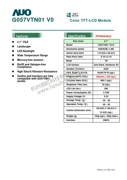
G057VTN01 V0 Color TFT-LCD Module5.7” VGA Landscape LED BacklightWide Temperature Range Mercury-free solution RoHS and Halogen-freeComplianceHigh Shock/Vibration Resistance Outline and Interface are fullycompatible with G057VN01 serials(Preliminary)Size (inch)5.7” ModelG057VN01 V210 Resolution (pixel) 640(RGB) x 480 Active Area (mm) 115.2(H) x 86.4(V)Pixel Pitch (mm) 0.18 x 0.18Mode TNLCD Surface Anti-Glare, Hardness 3HNumber of Colors 262K View Angle (L/R/U/D) 80/80/70/70 (typ.) Brightness(nit) (25℃) 500(min.), 600 (typ.)Contrast Ratio (25℃) 800:1 (typ.) Response Time (ms) 25 (typ.) LED Life (hrs.)50K Power Consumption (W) 3.74W Supply Voltage (V) 3.3V Storage Temp. (℃) -30 ~ 85 Operation Temp. (℃) -30 ~ 85Outline Dimension (mm) 144.0(H) x 104.6(V) x12.3(D) (typ.) Weight (g) 150g (typ.), 165g (max.)InterfaceCMOSTFT- LCD Interface Signal Description:Note 1: “Low” stands for 0V. “High” stands for 3.3V. “NC” stands for ”No Connection”.TFT- LCD Signal (CN1): LCD Connector: ManufacturerStarconnConnector Model Number 089H33-000100-G2-R, compatible withIMSA-9637S-33Y902 & ELCO 08-6210--033-340-800+Pin# Symbol Pin# Symbol Pin# Symbol 1 GND 12 GND 23 B3 2 DOTCLK 13 G0 24 B4 3 NC 14 G1 25 B5 4 NC 15 G2 26 GND 5 GND 16 G3 27 DE 6 R0 17 G4 28 VDD 7 R1 18 G5 29 VDD 8 R2 19 GND 30 R/L 9 R3 20 B0 31 U/D 10 R4 21 B1 32 NC 11 R522B233GNDLED Backlight Unit (CN2): Backlight Connector:ManufacturerJSTConnector Model Number SM06B-SRKS-G-TBcompatible with JST SM06B-SRSS-TB (LS) (SN)Mating Connecter Model Number JST SHR-06V-BKHF-B or compatiblePin # Symbol Pin # Symbol 1 V LED 4 GND 2 V LED 5 PWM DIM 3GND6LED ON/OFFLED Light Bar Input (CN3): Light Bar Connector ManufacturerSTM or compatible Connector Model Number P24021P6 or compatible Mating Connecter Model NumberSM06B-SHLS-TF or compatiblePin # Symbol Pin Description Cable color1 AN1 Channel 1 LED anode Red2 AN2 Channel 2 LED anode Red3 AN3 Channel 3 LED anode Red4 CA1 Channel 1 LED cathode White5 CA2 Channel 2 LED cathode Blue6 CA3Channel 3 LED cathodeBlack工业液晶屏www.hzxuhong.comReliability Test Criteria: ItemsRequired Condition Remark Temperature Humidity Bias40℃/90%,300HrNote 2 High Temperature Operation 85℃,300Hr Note 2 Low Temperature Operation -30℃,300Hr Note 2 High Temperature Storage 85℃,300 hours Note 2 Low Temperature Storage -30℃,300 hoursNote 2 Thermal Shock Test -20℃/30 min ,60℃/30 min ,100cyclesNote 2 Hot Start Test 85℃/1 Hr (min.), power on/off per 5 minutes, repeat 5 times Note 2 Cold Start Test -30℃/1 Hr (min.), power on/off per 5 minutes, repeat 5 times Note 2 Shock Test (Non-Operating) 50G, 20ms,Half-sine wave, (±X, ±Y , ±Z)Note 2Vibration Test (Non-Operating)(1)Random Wave 3.3rms, 0.5hr(X,Y,Z), 5~500hz (2)Sine Wave 6.8G, 10~400hz, 4hr40min (XYZ)Note 2ESDContact Discharge: ±8KV, 150pF(330Ω) 1sec, 8 points, 25times/pointAir Discharge: ±15KV, 150pF(330Ω) 1sec, 8 points, 25 times/pointNote 1,2Attitude TestOperating: 14,000 ft, Ramp: 2000 ft/min, 8hrs Non-operating: 40,000 ft, Ramp: 2000 ft/min, 24hrsNote 2Note1: According to EN61000-4-2 ESD class B criteria, some performance degradation is allowed. TFT-LCD module is self-recoverable, no data lost and no hardware failures after test. Note2:Water condensation is not allowed for each test items.Each test is done by new TFT-LCD module. Don’t use the same TFT-LCD module repeatedly for reliability test.The reliability test is performed only to examine the TFT-LCD module capability.To inspect TFT-LCD module after reliability test, please store it at room temperature and room humidity for 24 hours at least in advance.工业液晶屏www.hzxuhong.comVersion 0.2, Mar 2012Mechanical Characteristics:工业液晶屏www.hzxuhong.com。
(V) Preliminary Specifications() Final SpecificationsModule 12.1 Inch Color TFT-LCD Model Name G121SN01 V3Customer DateChecked &Approved by______ Note: This specification is subject to change without notice. Approved by Date Debbie Chiu 2007/11/07 Prepared bySam Chen___ 2007/11/07 General Display Business Division / AU Optronics CorporationContents1. Operating Precautions (4)2. General Description (5)2.1 Display Characteristics (5)2.2 Optical Characteristics (6)3. Functional Block Diagram (9)4. Absolute Maximum Ratings (10)4.1 Absolute Ratings of TFT LCD Module (10)4.2 Absolute Ratings of Environment (10)5. Electrical Characteristics (11)5.1 TFT LCD Module (11)5.2 Backlight Unit (13)6. Signal Characteristic (15)6.1 Pixel Format Image (15)6.2 Scanning Direction (15)6.3 Signal Description (16)LVDS Signal Format:6.4 The Input Data Format (17)6.4 The Input Data Format (18)6.5 Interface Timing (19)6.6 Power ON/OFF Sequence (20)7. Connector & Pin Assignment (21)7.1 TFT LCD Module: LVDS Connector (21)7.2 Backlight Unit: Lamp Connector (21)8. Reliability Test Criteria (22)9. Mechanical Characteristics (23)9.1 LCM Outline Dimension (Front View) (23)9.2 LCM Outline Dimension (Rear View) (24)9.3 Screw Hole Depth and Center Position (25)10. Label and Packaging (26)10.1 Shipping Label (on the rear side of TFT-LCD display) (26)10.2 Carton Package (26)11. Safety (27)11.1 Sharp Edge Requirements (27)11.2 Materials (27)11.3 Capacitors (27)11.4 National T est Lab Requirement (27)Record of RevisionVersion and Date Page Old Description New Description Remark0.0 2007/11/07 All First Draft All1. Operating Precautions1) Since front polarizer is easily damaged, please be cautious and not to scratch it.2) Be sure to turn off power supply when inserting or disconnecting from input connector.3) Wipe off water drop immediately. Long contact with water may cause discoloration or spots.4) When the panel surface is soiled, wipe it with absorbent cotton or soft cloth.5) Since the panel is made of glass, it may be broken or cracked if dropped or bumped on hard surface.6) Since CMOS LSI is used in this module, take care of static electricity and insure human earth whenhandling.7) Do not open nor modify the module assembly.8) Do not press the reflector sheet at the back of the module to any direction.9) In case if a module has to be put back into the packing container slot after it was taken out from thecontainer, do not press the center of the CCFL Reflector edge. Instead, press at the far ends of the CCFL Reflector edge softly. Otherwise the TFT Module may be damaged.10) At the insertion or removal of the Signal Interface Connector, be sure not to rotate nor tilt the InterfaceConnector of the TFT Module.11) After installation of the TFT Module into an enclosure (Notebook PC Bezel, for example), do not twist norbend the TFT Module even momentary. At designing the enclosure, it should be taken into consideration that no bending/twisting forces are applied to the TFT Module from outside. Otherwise the TFT Module may be damaged.12) Cold cathode fluorescent lamp in LCD contains a small amount of mercury. Please follow local ordinances orregulations for disposal.13) Small amount of materials having no flammability grade is used in the LCD module. The LCD module should besupplied by power complied with requirements of Limited Power Source (IEC60950 or UL1950), or be applied exemption.14) The LCD module is designed so that the CCFL in it is supplied by Limited Current Circuit (IEC60950 or UL1950).Do not connect the CCFL in Hazardous Voltage Circuit.15) Severe temperature condition may result in different luminance, response time and lamp ignition voltage.16) Continuous operating TFT-LCD display under low temperature environment may accelerate lamp exhaustion andreduce luminance dramatically.17) The data on this specification sheet is applicable when LCD module is placed in landscape position.18) Continuous displaying fixed pattern may induce image sticking. It’s recommended to use screen saver or shufflecontent periodically if fixed pattern is displayed on the screen.2. General DescriptionG121SN01 V3 is a Color Active Matrix Liquid Crystal Display composed of a TFT-LCD display, a driver circuit, and a backlight system. The screen format is intended to support SVGA (800(H) x 600(V)) screen and 16.2M (RGB8-bits) or 262K colors (RGB 6-bits). All input signals are LVDS interface compatible. Inverter card of backlight is not included.G121SN01 V3 is designed for industrial display applications.2.1 Display CharacteristicsThe following items are characteristics summary on the table under 25 ℃ condition:Items Unit SpecificationsScreen Diagonal [inch] 12.1Active Area [mm] 246.0(H) x 184.5(V)Pixels H x V 800x3(RGB) x 600Pixel Pitch [mm] 0.3075 x 0.3075Pixel Arrangement R.G.B. Vertical StripeDisplay Mode TN, Normally WhiteNominal Input Voltage VDD [Volt] 3.3 typ.Typical Power Consumption [Watt] 7.8W (64 Gray Bar Pattern, exclude inverter)Weight [Grams] 660g (typ.)Physical Size [mm] 279.0(H)x 209.0(V) x 11.0(D) (typ.)Electrical Interface 1 channel LVDSSurface Treatment AG, Hardness 3HSupport Color 16.2M/262K colorsTemperature RangeOperatingStorage (Non-Operating) [o C][o C]-30 to +85 (+85℃as panel surface temperature)-30 to +85RoHS Compliance RoHS Compliance2.2 Optical CharacteristicsThe optical characteristics are measured under stable conditions at 25℃ (Room Temperature): Item Unit Conditions Min. Typ. Max. NoteWhite Luminance [cd/m2] IRCFL= 6.0mA(center point)320 400 - 1Uniformity 13 Points - 1.25 1.60 1, 2, 3,Contrast Ratio - 600 - 4[msec] Rising - 10 20 5[msec] Falling - 2530 Response Time[msec] Rising + Falling - 35 50 5 6[degree] [degree] Horizontal (Right)CR = 10 (Left)60607070--6Viewing Angle[degree] [degree]Vertical (Upper)CR = 10 (Lower)45555060--6 Red x 0.590 0.620 0.650Red y 0.310 0.340 0.370Green x 0.275 0.305 0.335Green y 0.555 0.585 0.615Blue x 0.115 0.145 0.175Blue y 0.112 0.115 0.118White x 0.283 0.313 0.343Color / ChromaticityCoordinates(CIE 1931)%White y 0.299 0.329 0.359 Color Gamut 55Note 1: Measurement methodEquipment Pattern Generator, Power Supply, Digital Voltmeter, Luminance meter (SR_3 or equivalent)Aperture1with 50cm viewing distance ∘Test Point Center Environment < 1 luxNote 2: Definition of 13 points positionNote 3: The luminance uniformity of 13 points is defined by dividing the minimum luminance values by the maximum test point luminance.δW13 = Maximum Brightness of Thirteen PointsMinimum Brightness of Thirteen PointsModule Driving EquipmentNote 4: Definition of contrast ratio (CR):Note 5: Definition of response time:The output signals of photo detector are measured when the input signals are changed from “White ” to “Black ” (falling time) and from “Black ” to “White ” (rising time), respectively. The response time interval is between 10% and 90% of amplitudes. Please refer to the figure as below.Note 6: Definition of viewing angleViewing angle is the measurement of contrast ratio 10, at the screen center, over a 180° horizontal and 180°≧vertical range (off-normal viewing angles). The 180° viewing angle range is broken down as below: 90° (θ) horizontal left and right, and 90° (Φ) vertical high (up) and low (down). The measurement direction is typically perpendicular to the display surface with the screen rotated to its center to develop the desired measurement viewing angle.Contrast ratio (CR)=Brightness on the “White ” state Brightness on the “Black ” state3. Functional Block DiagramThe following diagram shows the functional block of the 12.1 inch color TFT/LCD module:LVDS Connector: MSB240420-EMating Type:P240420 or compatibleLamp Connector: JST BHR-03VS-1Mating Type:SM03(4.0)B-BHS-1-TB4. Absolute Maximum Ratings4.1 Absolute Ratings of TFT LCD ModuleItem Symbol Min Max Unit Logic/LCD Drive Vin -0.3 +3.6 [Volt]4.2 Absolute Ratings of EnvironmentItem Symbol Min Max Unit Operating Temperature TOP -30 +85 [o C] Operation Humidity HOP 8 95 [%RH] Storage Temperature TST -30 +85 [o C] Storage Humidity HST 5 95 [%RH] Note: Maximum Wet-Bulb should be 39℃ and no condensation.5. Electrical Characteristics5.1 TFT LCD Module5.1.1 Power SpecificationSymbol Parameter Min Typ Max Units RemarkVDD Logic/LCD DriveVoltage3.0 3.3 3.6 [Volt]IDD VDD Current - 285 325 [mA] VDD=3.3V, All Black PatternI rush LCD Inrush Current - - 1.5 [A] Vin=3.3V, With Black Pattern,Rising time=500us, PDD VDD Power - 0.94 1.07 [Watt] VDD=3.3V, All Black PatternVDDrp Allowable Logic/LCDDrive Ripple Voltage - 100[mV]p-pVDDns Allowable Logic/LCDDrive Ripple Noise 100[mV]p-p5.1.2 Signal Electrical CharacteristicsInput signals shall be low or Hi-Z state when VDD is off.Note: LVDS Signal Waveform.Symbol ItemMin. Typ. Max. Unit Remark|VID | Input Differential Voltage250 350 450 [mV]VICM Differential Input Common Mode Voltage1.0 1.252.0 [V] VTH Differential Input High Threshold - - 100 [mV] VCM=1.25V VTL Differential Input Low Threshold-100 - - [mV] VCM=1.25VCLKClock frequency304050MHz5.2 Backlight Unit5.2.1 Parameter guideline for CCFLFollowing characteristics are measured under a stable condition using an inverter at 25 (Room Temperature):℃Symbol ParameterMin. T yp. Max. UnitRemark IRCFLCCFL operation range3 6 6.5 [mA] rms (T a=25oC) Note 1, 2 FCFL CCFL Frequency 40 55 60 [KHz] (T a=25o C) Note 3 ViCFL 0oC) (reference) CCFL Ignition Voltage - 930 1,120 [Volt] rms (T a= 0o C) ViCFL (25o C) (reference) CCFL Ignition Voltage -770930[Volt] rms (T a=25o C)PCFL CCFL Power consumption (inverter excluded) 3.8 6.7 7.7 [Watt] (T a=25oC) Note 4 Lamp Life50,000-Hrs(T a=25oC) Note 2 IRCFL = 6mANote 1: IRCFL is defined as the return current of an inverter. (In Figure 1)(Figure 1: Measurement of return current)A stable IRCFL is a current without flicker or biasing waveform provided by inverter that ensures the backlight perform to its specification. The ideal sine waveform should be symmetric in positive and negative polarities and the asymmetry rate of the inverter waveform should be below 10%.ReferenceDC Bias = (| Ip – I-p| / Irms ) x 100 % <10%Crest Factor = Ip or (I-p) / Irms should have the range within 1.414 + 10%It is recommended to use the inverter with detection circuit ( ie: balance and protection circuit) to avoid overvoltage, overcurrent, or mismatching waveform.Note 2: The definition of lamp life means when any of following conditions happen:a) Luminance falls to 50% or less of the initial value.b) Normal lighting is no more available (flickering, pink lighting, no lighting, etc.)c) Lamp voltage or lighting start voltage exceeds the specified value.Lamp life time shortens according toa) Placing methodology: mercury is unevenly distributed in portrait mountingb) Environmental condition: low temperature reduces the presence of mercury vapor, which results inapproximately lamp life of 1,000 hoursc) CCFL surface temperature: Presence of gradient in lamp surface temperature causes uneven mercurymigrationd) Inverter design: its resonance capacitor should be fine-tuned with the impedance of CCFLe) Over driving current ( > 6.5 mA) shortens lamp life time dramatically.Note 3: CCFL frequency should be carefully determined to avoid interference between inverter and TFT LCD. Higher frequency will induce higher leakage current and further impact lamp life.Note 4: Calculator value for reference (IRCFLxVCFLx2=PCFL).Note 5: The display is with dual lamp design, and the CCFL current in above table refers to each lamp6. Signal Characteristic 6.1 Pixel Format ImageFollowing figure shows the relationship between input signal and LCD pixel format.6.2 Scanning DirectionThe following figures show the image seen from the front view. The arrow indicates the direction of scan.Fig. 1 Normal scan (Pin19 = GND/NC)Fig. 2 Reverse scan (Pin19 = High)6.3 Signal DescriptionThe module uses a LVDS receiver embedded in AUO’s ASIC. LVDS is a differential signal technology for LCD interface and a high-speed data transfer device. Mating LVDS transmitter: THC63LVDM83A or equivalent device Pin Assignment:Pin# Signal Name Description1VCC 3.3V Power Supply2VCC 3.3V Power Supply3GND GND46-8Bit SEL Select 6 or 8 Bits LVDS Input (VCC:8Bits ; GND/NC: 6Bits)5RIN0-Negative(-) LVDS differential data input6RIN0+Positive(+) LVDS differential data input7GND GND8RIN1-Negative(-) LVDS differential data input9RIN1+Positive(+) LVDS differential data input10GND GND11RIN2-Negative(-) LVDS differential data input12RIN2+Positive(+) LVDS differential data input13GND GND14CLKIN-Clock Signal(-)15CLKIN+Clock Signal(+)16GND GND17RIN3-Negative(-) LVDS differential data input(Used for 8Bits LVDS Input; NC for 6Bits)18RIN3+Positive(+) LVDS differential data input(Used for 8Bits LVDS Input; NC for 6Bits)19REVERSE Display Reversed Function(VCC: Display Reverse; GND/NC: Normal Display)20NC/GND AUO Test Function Pin(Do not set this pin to High)Note1: Pin19 can be used for enabling “reverse scan” function.Refer to section 6.1 for scanning direction.Signal Description:Signal Name DescriptionRxIN0-, RxIN0+ LVDS differential data input (Red0-Red5, Green0)RxIN1-, RxIN1+ LVDS differential data input (Green1-Green5, Blue0-Blue1)RxIN2-, RxIN2+ LVDS differential data input (Blue2-Blue5, Hsync, Vsync, DE)CKIN-, CKIN+ LVDS differential clock inputReverse High: Reverse Display; NC/GND: Normal DisplayVDD +3.3V Power SupplyGND GroundNC No ConnectionNote: Input signals shall be low or Hi-Z state when VDD is off.LVDS Signal Format: 6/8 SEL = Low (GND)6/8 SEL = High6.4 The Input Data FormatSignal Name Description+RED5 +RED4 +RED3 +RED2 +RED1 +RED0 Red Data 5 (MSB)Red Data 4Red Data 3Red Data 2Red Data 1Red Data 0 (LSB)Red-pixel DataRed-pixel DataEach red pixel’s brightness data consists of these6 bits pixel data.+GREEN5 +GREEN4 +GREEN3 +GREEN2 +GREEN1 +GREEN0 Green Data 5 (MSB)Green Data 4Green Data 3Green Data 2Green Data 1Green Data 0 (LSB)Green-pixel DataGreen-pixel DataEach green pixel’s brightness data consists of these6 bits pixel data.+BLUE5 +BLUE4 +BLUE3 +BLUE2 +BLUE1 +BLUE0 Blue Data 5 (MSB)Blue Data 4Blue Data 3Blue Data 2Blue Data 1Blue Data 0 (LSB)Blue-pixel DataBlue-pixel DataEach blue pixel’s brightness data consists of these6 bits pixel data.CLK Data Clock The typical frequency is 40MHz. The signal isused to strobe the pixel data and DE signals.All pixel data shall be valid at the falling edge whenthe DE signal is high.DE Display Timing This signal is strobed at the falling edge of CLK.When the signal is high, the pixel data shall be validto be displayed.VSYNC Vertical Sync The signal is synchronized to CLK.HSYNC Horizontal Sync The signal is synchronized to CLK.Note: Output signals from any system shall be low or Hi-Z state when VDD is off.6.5 Interface Timing6.5.1 Timing CharacteristicsDE only modeParameter Symbol Min. Typ. Max. Unit ConditionClock frequency 1/ T Clock 33.6 39.8 48.3 MHzPeriod T V 608 628 650 Active T VD 600 600 600 Vertical SectionBlanking T VB 8 28 50 T LinePeriod T H 920 1056 1240 Active T HD 800 800 800 Horizontal SectionBlankingT HB120256440T ClockNote1: Frame rate is 60 Hz.Note2: Typical value refer to VESA Standard6.5.2 Input Timing Diagram6.6 Power ON/OFF SequenceVDD power and lamp on/off sequence is as below. Interface signals are also shown in the chart. Signals from any system shall be Hi-Z state or low level when VDD is off.VDD0V0V0VPower ON/OFF sequence timingValueUnitsParameterMin. Typ. Max.T10.5 - 10 msT2 0 - 50 msT3 0 - 50 msT4 0 - 10 msT5 200 - msT6 200 - msT7 500 - - MsThe above on/off sequence should be applied to avoid abnormal function in the display. Please make sure to turn off the power when you plug the cable into the input connector or pull the cable out of the connector.7. Connector & Pin AssignmentPhysical interface is described as for the connector on module. These connectors are capable of accommodating the following signals and will be following components.7.1 TFT LCD Module: LVDS ConnectorConnector Name / Designation Signal ConnectorManufacturer STMConnector Model Number MSB240420-EMating Model Number P240420 or compatibleMating LVDS transmitter: THC63LVDM83A or equivalent device7.2 Backlight Unit: Lamp ConnectorConnector Name / Designation Lamp ConnectorManufacturer JSTConnector Model Number JST BHR-03VS-1 or compatibleMating Model Number JST SM03(4.0)B-BHS-1-TBPin no. Symbol Function Remark1 H CCFL power supply (H.V.) Cable color: Pink2 NC No connection3 L CCFL power supply (GND) Cable color: White8. Reliability Test CriteriaItems Required Condition Note High TemperatureOperation 85, 240Hrs℃ (center point of panel surface) Note 1, 2, 3 Low TemperatureOperation -30, 240Hrs℃Note 1, 2, 3 Hot Storage 85, 240Hrs℃Note 1, 2, 3 Cold Storage -30, 240Hrs℃Note 1, 2, 3High temperature & high humidity operation 50, 90%RH, 240Hrs℃(No condensation)Note 1, 2, 3Shock Test(Non-Operating) 50G/11ms, ±X, ±Y, ±Z, half-Sin, one time Note 1, 2, 3Vibration Test (Non-Operating) 1.5G, random 10H Z ~ 200H Z ~ 10H Z30 minutes for each Axis (X, Y, Z), 15min/SweepNote 1, 2, 3On/off test On 10sec/OFF 10 sec, 30,000 cycles Note 1, 2, 3 Contact Discharge: Max±8KV, 150pF(330Ω) 1sec, 8 points, 25times/point.ESDAir Discharge: Max ±15KV, 150pF(330Ω) 1sec, 8 points, 25times/pointNote 3, 4Thermal shock (non-operation) 1. -20±3…30minutes℃℃60±3…30minutes℃℃2. 100 cycles3. T emperature transition time within 5 minutesNote 1, 2, 3Attitude Test Operation:14,000ft / 8hrsNon-Operation: 40,000ft / 24hrsNote 3Note 1: Evaluation should be tested after storage at room temperature for one hour.Note 2: There should be no change which might affect the practical display function when the display quality test is conducted under normal operating condition.Note 3: Judgment: 1. Function OK 2. No serious image quality degradationNote 4: According to EN61000-4-2 , ESD class B: Some performance degradation allowed. No data lost, self-recoverable. No hardware failures.9.3 Screw Hole Depth and Center PositionScrew type: M3 screwScrew hole minimum depth, from side surface =2.7mm (See drawing) The Max. Diameter of the mounting screw head is 6.0mmScrew Torque: Maximum 6.0 kgf-cm10. Label and Packaging10.1 Shipping Label (on the rear side of TFT-LCD display)10.2 Carton PackageMax capacity: 20 TFT-LCD modules per carton.Max weight: 17 kg per cartonOutside dimension of carton: 576(L) mm x 326(L) mm x 420(H) mm11. Safety11.1 Sharp Edge RequirementsThere will be no sharp edges or comers on the display assembly that could cause injury.11.2 MaterialsToxicityThere will be no carcinogenic materials used anywhere in the display module. If toxic materials are used, they will be reviewed and approved by the responsible AUO toxicologist.11.3 CapacitorsIf any polarized capacitors are used in the display assembly, provisions will be made to keep them from being inserted backwards.11.4 National Test Lab RequirementThe display module will satisfy all requirements for compliance to:UL 60950 U.S.A. Information Technology Equipment。
友达光电产品命名规则友达光电,简称Auo,命名规则:B121EW01,B170PW03第一位表示用途,2-4位为尺寸,5位为分辨率,6位为宽屏/普屏(在非a-Si技术中标注所用技术),最后两位为产品代次,注:部分产品还有空格后加注V*(如B121EW07 V0)还没有弄明白其含义。
具体细明如下:第一位表示用途B;表示笔记型电脑用G:表示工业用T:表示电视用M:表示桌上电脑用H:表示手机用C:表示车载设备用A:表示可移动产品(数码相机,PDA等)第二到四位表示尺寸例如:121代表12.1’ 170代表17’第五位表示分辨率I:128*128Q:320*240A:280*220B:640*240C:160*234 /480*240D:960*240F:480*234V:640*480S:1680*1050E:1280*800P:1440*900X:1024*768 1366*768H:1920*1080U:1920*1200注:因为产品太多,目前总结这些可能有遗漏。
第六位表示普通屏幕和宽屏N:普通型W:宽屏型另外:在不用a-Si屏的情况下它代表所用技术L/T::代表低温多晶硅技术七八位表示产品代数:例如:01表示第一代产品,03表示第三代产品部分产品加空格后还有第九、十位,这个还没有弄明白其所代表的含义。
下面是AU部分产品名称及其对应型号用途说明。
笔记本电脑Wide Aspect RatioModel Size ResolutionB121EW01 12.1" WXGA (1280 x 800)B121EW03 12.1" WXGA (1280 x 800)B121EW04 12.1" WXGA (1280 x 800)B121EW07 V0 12.1" WXGA (1280 x 800)B133EW01 13.3" WXGA (1280 x 800)B141EW02 14.1" WXGA (1280 x 800)B141PW01 14.1" WXGA+ (1440 x 900)B154EW02 V1 15.4" WXGA (1280 x 800)B154PW04 V0 15.4" WXGA+ (1440 x 900) B170PW03 17'' WXGA+ (1440 x 900) B170PW07 17" WXGA+ (1440 x 900) B170UW02 17" WUXGA (1920 x 1200) B170UW02 V0 17" WUXGA (1920 x 1200) Standard Aspect RatioModel Size ResolutionB141XG09 V3 14.1" XGA (1024 x 768) B150XG02 V4 15'' XGA (1024 x 768)液晶电视Model Size ResolutionT370HW02 37" Full HD (1920 x 1080) T420HW01 42" Full HD (1920 x 1080)T420HW01 V3 42" Full HD (1920 x 1080) T460HW02 46" Full HD (1920 x 1080)T645HW01 65 Full HD (1920 x 1080) HDModel Size ResolutionT200XW02 20" WXGA (1366 x 768) T230XW01 23" WXGA (1366 x 768) T260XW02 26" WXGA (1366 x 768) T315XW01 32" WXGA (1366 x 768) T315XW02 32" WXGA (1366 x 768) T370XW01 37" WXGA (1366 x 768) T370XW02 37" WXGA (1366 x 768) T420XW01 42" WXGA (1366 x 768)桌上型电脑Wide Aspect RatioModel Size ResolutionM185XW01 V0 18.5" 1366 x 768M190PW01 V0 19" WXGA+ (1440 x 900) M201EW02 V8 20.1" WSXGA+ (1680 x 1050)M215HW01 V0 21.5" 1920 x 1080M220EW01 V0 22" WSXGA+ (1680 x 1050) M240UW04 V0 24" WUXGA (1920 x 1200)M240HW01 V0 24" 1920 x 1080Standard Aspect RatioModel Size ResolutionM170EG01 VD 17 SXGA (1280 x 1024一般工业用显示器G057QN01 5.7 QVGA (320 x 240)G057VN01 5.7 VGA (640 x 480)G065VN01 V0 6.5 VGA (640 x 480)G065VN01 V1 6.5 VGA (640 x 480)G084SN03 V1 8.4 SVGA (800 x 600)G084SN05 V7 8.4 SVGA (800 x 600)G104VN01 10.4 VGA (640 x 480)G104SN02 V1 10.4 SVGA (800 x 600)G104SN03 V1 10.4 SVGA (800 x 600)G121SN01 V1 12.1 SVGA(800x600)G121SN01 V3 12.1 SVGA (800x600)G150XG01 V1 15 XGA (1024 x 768)G150XG02 V0 15 XGA (1024 x 768)G150XG03 V2 15 XGA (1024 x 768)G420XW01 V0 42 WXGA (1366 x 768)G420XW02 V0 42 WXGA (1366 x 768)P645HW01 V0 65 FHD (1920 x 1080)P520HW01 V0 52 FHD (1920 x 1080)G220SW01 V0 22 1680 x 1050移动电话Model Size ResolutionH016IN01 1.56" 128 R.G.B. x 128 H167IN01 1.67" 128 R.G.B. x 160 H176HN01 1.76" 176 R.G.B. x 220 H177IN01 1.77" 128 R.G.B. x 160 H177IN02 1.77" 160 R.G.B. x 128 H019HN01 1.88" 176 R.G.B. x 220 H200HN01 2.0" 176 R.G.B. x 220 H283QN01 2.83" 240 R.G.B. x 320 LTPSModel Size ResolutionH180QT01 1.8" 240 R.G.B. x 320H200QT01 2.0" 240 R.G.B. x 320H220QT02 2.2" 240 R.G.B. x 320H222QL01 2.22" 240 R.G.B. x 320H241QL01 2.4" 240 R.G.B. x 320H283VL01 2.83" VGA 480 R.G.B. x 640数码相机摄象机A015AN04 1.5" 280 x 220A017CN01 1.7" 480 x 240A020CN01 2.0" 480 x 240A020BL01 2.0" LTPS 640 x 240A024CN02 2.4" 480 x 234A025BN01 2.5" 640 x 240A025DL02 2.5'' LTPS 960 x 240A027CW00 2.7" 480 x 234A027DL01 2.7" LTPS 960 x 240A027DN01 2.7" 960 x 240A030DL01 3.0" LTPS 960 x 240A030DL02 3.0" LTPS 960 x 240车载产品C036QN02 3.6" 320 R.G.B. x 240 C065GW01 6.5" 400 R.G.B. x 234 C065VL01 6.5" 800 R.G.B. x 480 C070FW01 7.0" 480 R.G.B. x 234 C070VW02 7.0" 800 R.G.B. x 480 C080VW02 8.0" 800 R.G.B. x 480 Portable Media PlayerModel Size ResolutionA036QN02 3.6 320 R.G.B. x 240 A070FW03 7.0" 480 R.G.B. x 234 A070VW02 7.0" 800 R.G.B. x 480 A085FW01 8.5" 480 R.G.B. x 234 A102VW01 10.2" 800 R.G.B. x 480一般应用Model Size ResolutionA035CN02 3.5" 160 R.G.B. x 234A040CN01 4.0" LED 160 R.G.B. x 234A056DN01 5.6" 320 R.G.B. x 234奇美电子产品命名规则奇美电子,简称CMO,命名规则分两种1,大尺寸2,中小尺寸大尺寸命名规则第一位表示用途,第二位到四位为尺寸,第五位为分辨率,最后一位为产品代次,共六位,部分产品还有空格后加七八九位。
CUSTOMER APPROVAL SHEETCompany NameMODEL A104SN03 V1CUSTOMER APPROVED Title : Name :□ APPROVAL FOR SPECIFICATIONS ONLY (Spec. Ver. )□ APPROVAL FOR SPECIFICATIONS AND ES SAMPLE (Spec. Ver. )□ APPROVAL FOR SPECIFICATIONS AND CS SAMPLE (Spec. Ver. )□ CUSTOMER REMARK :AUO PM :P/N :Comment :1 Li-Hsin Rd. 2. Science-Based Industrial ParkHsinchu 300, Taiwan, R.O.C.Tel: +886-3-500-8899Doc. version : 0.7Total pages : 34Date : 2009/04/27Product Specification10.4" COLOR TFT-LCD MODULE Model Name:A104SN03 V1Planned Lifetime: From 2008/Dec To 2010/Dec Phase-out Control:From 2010/Jul To 2010/Dec EOL Schedule: 2010/Decary Specification< >Final SpecificationNote: The content of this specification is subject to change.© 2009 AU Optronics All Rights Reserved, Do Not Copy.Page: 1/34Record of RevisionVersion Revise Date Page Content0.0 2008/10/29All First Draft0.1 2008/11/1224 Update Response time29 Update drawing0.2 2009/01/07 4 Update drawing17 Update Register Table18 Delete R1 setting0.3 2009/1/16 4 Update drawing10 Delete extra Electrical DC Characteristics32 Add Application Circuit0.4 2009/02/048 Delete extra note0.5 2009/03/1512 Add VCOMin22 Delete Power on R133 Update Application Circuit0.6 2009/03/3125 Update Contrast ratio0.7 2009/4/27 19 Update Register Table & Register DescriptionPage: 2/34ContentsA.General Information (3)B.Outline Dimension (4)1.TFT-LCD Module (4)C.Electrical Specifications (6)1. TFT LCD Panel Pin Assignment (6)2. Backlight Pin Assignment (9)3. Absolute Maximum Ratings (9)3. Electrical DC Characteristics (10)4. Electrical AC Characteristics (14)5. Serial Interface Characteristics (17)6. Power On/Off Characteristics (22)D.Optical Specification (25)E.Reliability Test Items (28)F.Packing and Marking (31)1. Packing Form (31)2. Module/Panel Label Information (32)3. Carton Label Information (32)G.Application Note (33)Application Circuit (33)H.Precautions (34)Page:3/34A. General InformationThis product is for portable DVD and digital photo frame application.NO. ItemUnit SpecificationRemark1 Screen Sizeinch 10.4(Diagonal)2 Display Resolutiondot800RGB(W)x600(H)3 Overall Dimensionmm 228.4(W)x175.4(H)x6.2(D)Note 1 4 Active Area mm211.2(W)x158.4(H)5 Pixel Pitchmm 0.264(W)x0.264(H) 6 Color Configuration-- R. G. B. Stripe Note 27 Color Depth -- 16.7M ColorsNote 3 8 NTSC Ratio% 509Display Mode-- Normally White 10 Panel surface Treatment --Anti-Glare, 3H11 Weightg400±2012 Panel Power ConsumptionW 0.43Note 4 13 Backlight Power Consumption W 2.97 14 Viewing direction6 o’clock (gray inversion)Note 1: Not include blacklight cable and FPC. Refer next page to get further information. Note 2: Below figure shows dot stripe arrangement.Note 3: The full color display depends on 24-bit data signal (pin 4~27). Note 4: Please refer to Electrical Characteristics chapter.( 1…………...……………..600 )V e r s i o n :0.7P a g e : 4/34I G H T S S T R I C T L Y R E S E R V E D . A N Y P O R T I O N O F T H I S P A P E R S H A L L N O T B E R E P R O D U C E D , C O P I E D , O R T R A N S F O R M E D T O A N Y O T H E R F O W I T H O U T P E R M I S S I O N F R O M A U O P T R O N I C S C O R P .O u t l i n e D i m e n s i o n1. T F T -L C D M o d u l eV e r s i o n :0.7P a g e : 5/34I G H T S S T R I C T L Y R E S E R V E D . A N Y P O R T I O N O F T H I S P A P E R S H A L L N O T B E R E P R O D U C E D , C O P I E D , O R T R A N S F O R M E D T O A N Y O T H E R F O W I T H O U T P E R M I S S I O N F R O M A U O P T R O N I C S C O R P .Page: 6/34 C. Electrical Specifications1. TFT LCD Panel Pin AssignmentRecommended connector : HRS FH28-60S-0.5SHPin no Symbol I/O Description Remark1 AGND P Ground for analog circuit2 AVDD P Analog power supply voltage3 VDDIO P Digital interface supply voltage4 R0 I Red data input (LSB)5 R1 I Red data input6 R2 I Red data input7 R3 I Red data input8 R4 I Red data input9 R5 I Red data input10 R6 I Red data input11 R7 I Red data input (MSB)12 G0 I Green data input (LSB)13 G1 I Green data input14 G2 I Green data input15 G3 I Green data input16 G4 I Green data input17 G5 I Green data input18 G6 I Green data input19 G7 I Green data input (MSB)20 B0 I Blue data input (LSB)21 B1 I Blue data input22 B2 I Blue data input23 B3 I Blue data input24 B4 I Blue data input25 B5 I Blue data input26 B6 I Blue data input27 B7 I Blue data input (MSB)28 DCLK I Data clock input29 DE I Data enable signal30 HSYNC I Horizontal sync input. (Negative polarity)31 VSYNC I Vertical sync input. (Negative polarity)32 SCL I Serial communication clock input33 SDA I Serial communication data input34 CSB I Serial communication chip selectPage:7/3435NC-For test, do not connect (Please leave it open)36 VDDIO P Digital interface supply voltage 37 NC - For test, do not connect (Please leave it open)38 GND P Ground for digital circuit 39 AGND P Ground for analog circuit 40 AVDDP Analog power supply voltage41VCOMin IFor external VCOM DC input 42 DITH IDithering setting DITH = "L" 6bit resolution(LSB last 2 bits of input data turncated)DITH = "H" 8bit resolution(Default setting)43 NC- For test, do not connect (Please leave it open) 44 VCOM O connect a capacitor 45 V10 I Gamma correction voltage reference 46 V9 I Gamma correction voltage reference 47 V8 I Gamma correction voltage reference 48 V7 I Gamma correction voltage reference 49 V6 I Gamma correction voltage reference 50 V5 I Gamma correction voltage reference 51 V4 I Gamma correction voltage reference 52 V3 I Gamma correction voltage reference 53 V2 I Gamma correction voltage reference 54 V1IGamma correction voltage reference55 NC - For test, do not connect (Please leave it open)56 VGH P Positive power for TFT57 VDDIO P Digital interface supply voltage 58 VGL P Negative power supply for Gate driver.59 GND P Ground for digital circuit 60 NC-For test, do not connect (Please leave it open)I: Input; P: PowerPage: 8/34.Page:9/342. Backlight Pin AssignmentRecommended connector : JOIN TEK JT1025-1021Pin no Symbol I/O Description Remark1 VLED+ P Backlight LED anode2VLED-PBacklight LED cathode3. Absolute Maximum RatingsItemSymbol Conditio Min. Max. Unit Remark VDDIO GND=0 -0.5 5 V Digital Power Supply AVDDAGND=0 -0.5 15 VAnalog power supplyVGH -0.3 42 V Gate driver supply voltage VGL GND=0-20 0.3 V Gate driver supply voltage Power voltageVGH -VGL- 40V Gate driver supply voltageV I -0.3 VDDIO+0.3 VNote 1 Input signal voltageVCOMin 0 5 VVCOM DC VoltageOperating Topa -10 60 StorageTstg-2070Note 1: Functional operation should be restricted under ambient temperature.Note 2: Maximum ratings are those values beyond which damages to the device may occur. Functional operation should be restricted to the limits in the Electrical Characteristics chapter.Page: 10/343. Electrical DC Characteristicsa. Typical Operation Condition (AGND =GND = 0V)Item Symbol Min. Typ.Max. Unit RemarkVDDIO 3.0 3.3 3.6 V Digital Power SupplyAVDD 10.5 11 11.5 V Analog Power Supply Power VoltageVGH 14 15 16 V Positive power supply for gatedriverVGL -7.5 -7 -6.5 V Negative power supply forgate driver InputH Level VIH 0.7xVDDIO-- VDDIO VSignal Voltage L Level VIL GND -- 0.3xVDDIO VGamma referenceV1 ~ V5AVDD/2 - AVDD – 1V Note 1 voltage V6 ~ V10 1 - AVDD/2 VVCOMin V CDC 3.75 3.95 4.15 V Note 2 Note 1: Gamma suggested circuit is as followsPage: 11/34 Pin Voltage(V)AVDD 11V1 10V2 8.5V3 8V4 7.57V5 6.7V6 4.3V7 3.43V8 3V9 2.5V10 1Page: 12/34 Note2: Based on recommended Gamma 2.2 voltage.Page: 13/34b. Current Consumption (AGND=GND=0V)Parameter Symbol Condition Min. Typ. Max. Unit Remark Input current for VDDIO IVDDIO VDDIO = 3.3V 10 20 m A Note 1, 2 Input current for AVDD IAVDD AVDD = 11V 24 30 mA Note 1, 2 Input current for VGH IVGH VGH = 15V -- 0.4 0.6 mA Note 1, 2 Input current for VGL IVGL VGL = -7V -0.6 -0.4 -- mA Note 1, 2 Note 1:Test Condition is under typical Eletrical DC and AC characteristics.Note 2: Test pattern is the following picture.c. Backlight Driving ConditionsThe backlight (LED module, Note 1) is suggested to drive by constant current with typical value.Parameter Symbol Min. Typ. Max. Unit Remark LED light bar Current I L-- 300 -- mAPower Consumption P -- 3 3.21 W Note 1 LED Life Time L L10,000 -- -- Hr Note 2, 3 Note 1: The LED driving condition is defined for LED module (36 LED). The Voltage range will be 8.8V to 10.7V based on suggested driving current set as 300mA.Note 2: Define “LED Lifetime”: brightness is decreased to 50% of the initial value. LED Lifetime is restricted under normal condition, ambient temperature = 25℃and LED lightbar current =300mA.Note 3: If it uses larger LED lightbar current more than 300mA, it maybe decreases the LED lifetime.Page: 14/344. Electrical AC Characteristicsa. Signal AC CharacteristicsParameter Symbol Min. Typ. Max. Unit Remark DCLK duty cycle -- 40 50 60 % t cw / t DCLK x100% VSYNC setup time t vst0 -- -- nsVSYNC hold time t vhd 2 -- -- nsHSYNC setup time t hst 5 -- -- nsHSYNC hold time t hhd10 -- -- nsData setup time t dst 5 -- -- nsData hold time t dhd10 -- -- nsData enable set-up time t est 4 -- -- nsData enable hold time t ehd 2 -- -- nsPage:15/34b. Input TimingHS R[7:0]G[7:0]B[7:0]DCLKHorizontal input timing. (HV mode)DCLK DER[7:0]G[7:0]B[7:0]Horizontal TimingParameter Symbol Min. Typ. Max. Unit. RemarkDCLK frequency F DCLK 25 40 45 MHz DCLK periodT DCLK 22 25 40 ns Hsync period (= T HD + T HBL )T H 1026 1056 1183 DCLK Active AreaT HD - 800 - DCLK Horizontal blanking (= T HF + T HE )T HBL 226 256 383 DCLK Hsync front porchT HF 10 40 167 DCLK Delay from Hsync to 1st data input(= T HW + T HB )T HE216DCLKPage: 16/34 Hsync pulse width T HW 1 128 136 DCLKHsync back porch T HB80 88 215 DCLKHorizontal input timing (HV mode)Horizontal input timing (DE mode)Vertical TimingParameter Symbol Min. Typ. Max. Unit. Remark Vsync period (= T VD + T VBL) T V- 628 635 ThActive lines T VD- 600 - Th Vertical blanking (= T VF + T VE) T VBL- 28 35 ThVsync front porch T VF- 1 8 ThGD start pulse delay T VE- 27 - ThVsync pulse width T VW 1 3 16 ThHsync/Vsync phase shift T VPD 2 320 - DCLKPage: 17/34Vertical timing (HV mode)Vertical timing (DE mode)5. Serial Interface Characteristicsa. Serial Control Interface AC CharacteristicParameter Symbol Min. Typ. Max. Unit. Remark Serial data setup time T IST120 - - nsSerial data hold time T IHD120 - - nsCSB setup time T CST120 - - nsCSB hold time T CHD120 - - nsSerial clock high/low T SSW120 - - nsSerial clock T SCK320 - - nsDelay from CSB to VSYNC T CV 1 - - usChip select distinguish T CD 1 - - usSerial data output delay T ID- - 60 ns CL=20pFPage: 18/34b Serial Interface TimingThere is a total of 6 registers each containing several parameters. For a detailed description of the parameters refer to register table. The serial register has read/write function. D[15:12] are the register address, D[11] defines the read or write mode and D[10:0] are the data.Serial Interface Write sequence1. At power-on, the default values specified for each parameter are taken.2. If less than 16-bit data are read during the CS low time period, the data is cancelled.a. The write operation is cancelled.3. All items are set at the falling edge of the vertical sync, except R0[1:0].4. When GRB is activated through the serial interface, all registers are cleared, except the GRB value.5. The register setting values are valid when VCC already goes to high and after VSYNC starts.6. It is suggested that VSYNC, HSYNC, DCLK always exists in the same time. But if HSYNC, DCLK stops,only VSYNC operating, the register setting is still valid.7. If the chip goes to standby mode, the register value will still keep. MCU can wake up the chip only bychanging standby mode value from low to high.8. The register setting values are rewritten by the influence of static electricity, a noise, etc. to unsuitable value,incorrect operating may occur. It is suggested that the SPI interface will setup as frequently as possible.Page:19/34c. Register Table (Default Value)RegADDRESSR/WDATA No. D15 D14 D13 D12 D11 D10 D9D8D7D6 D5 D4 D3 D2 D1D0R0 0 0 0 0 0 (01)(01) (1)(0)(1) (1)(0)GRB (1)STB (1)R2 0 0 1 0 0 × × × HDL(80h)R3 0 0 1 1 0 × × (0) (0) (0) (0) (0) VDL(1000)R4 0 1 0 0 0 × × (1)(0) (0)(0) (1) (1111)R6 011×(0)EnGB12 (1)EnGB11 (1)EnGB10 (1)(0)(0)EnGB5 (1)EnGB4 (1)EnGB3 (1)(0)X: Reserved. Please set to “0”.<Note>:Sending serial commands periodically is recommended to improve ESD protection ability.d. Register Descriptiona. R0 setting AddressBitDescriptionDefault 0000 [10..0] Bits 10-9 AUO Internal Use 01 Bits7-8AUO Internal Use 01 Bit6 (DITH) Dithering function. 1 Bit5 AUO Internal Use 0 Bit4 AUO Internal Use 1 Bit3 AUO Internal Use. 1 Bit2 AUO Internal Use 0 Bit1 (GRB) Global reset.1Bit0 (STB) Standby mode setting.1Bit6 DITH function0 DITH off.1DITH on. (default)Bit1GRB function0 The controller is reset. Reset all registers to default value. 1Normal operation. (default)Bit0STB function0 T-CON and source driver are off. All outputs are set to GND.1Normal operation. (default)Address Bit Description Default 0010 [7..0] Bit7-0(HDL) Horizontal start pulse adjustment function80H Bit7-0 HDL function00h T HE = T HEtyp - 128 CLK period.80h T HE = T HEtyp. (default)FFh T HE = T HEtyp + 127 CLK period.c. R3 settingAddress Bit Description Default 0011[8..0]Bit8 AUO Internal Use0Bit7 AUO Internal Use0Bit6 AUO Internal Use 0Bit5 AUO Internal Use 0Bit4 AUO Internal Use 0Bit3-0(VDL) Vertical start pulse adjustment function 1000Bit3-0 VDL function0000 T VE = T VEtyp – 8 Hs period.0001 T VE = T VEtyp – 7 Hs period.0010 T VE = T VEtyp – 6 Hs period.0011 T VE = T VEtyp – 5 Hs period.0100 T VE = T VEtyp – 4 Hs period.0101 T VE = T VEtyp – 3 Hs period.0110 T VE = T VEtyp – 2 Hs period.0111 T VE = T VEtyp – 1 Hs period.1000 T VE = T VEtyp. (default)1001 T VE = T VEtyp – 1 Hs period.1010 T VE = T VEtyp – 2 Hs period.1011 T VE = T VEtyp – 3 Hs period.1100 T VE = T VEtyp – 4 Hs period.1101 T VE = T VEtyp – 5 Hs period.1110 T VE = T VEtyp – 6 Hs period.1111 T VE = T VEtyp – 7 Hs period.Address Bit Description Default 0110 [9..0] Bits9 AUO Internal Use 0Bits8(EnGB12)Gamma buffer Enable for V9 1Bits7(EnGB11)Gamma buffer Enable for V8 1Bits6(EnGB10)Gamma buffer Enable for V7 1Bits5 AUO Internal Use 0Bits4 AUO Internal Use 0Bits3(EnGB5) Gamma buffer Enable for V4 1Bits2(EnGB4) Gamma buffer Enable for V3 1Bits1(EnGB3) Gamma buffer Enable for V2 1Bits0 AUO Internal Use 0 Bitx EnGBx function0 Gamma buffer for VX is disabled (High Z).1 Gamma buffer is enabled. VX must be connected externally.Page: 22/346. Power On/Off Characteristicsa. Recommended Power On Register SettingADDRESS R/W DATARegNo.D15D14D13D12D11D10 D9 D8 D7 D6 D5 D4 D3 D2 D1 D0 R00000010 01 1 0 1 0 0 1 1 R2001000 0 0 80hR3001100 0 0 0 0 0 0 1000R4010000 0 1 1 00 1 1111R6011000 0 1 1 1 0 0 1 1 1 0Note : Start to provide SPI commend at least after 2 frame.1. Send R15 : 000h(Normal register bank) at first.2. Wait at least after more than one frame, send R0 : 4D1h(Global Reset)3. After send Global Reset, start to send R0 to R6 recommend register value.V e r s i o n :0.7P a g e : 23/34G H T S S T R I C T L Y R E S E R V E D . A N Y P O R T I O N O F T H I S P A P E R S H A L L N O T B E R E P R O D U C E D , C O P I E D , O R T R A N S F O R M E D T O A N Y O T H E R F O R M S W I T H O U T P E R M I S S I O N F R O M A U O P T R O N I C S C O R P .R e c o m m e n d e d P o w e r O n S e q u e n c eV e r s i o n :0.7P a g e : 24/34G H T S S T R I C T L Y R E S E R V E D . A N Y P O R T I O N O F T H I S P A P E R S H A L L N O T B E R E P R O D U C E D , C O P I E D , O R T R A N S F O R M E D T O A N Y O T H E R F O R M S W I T H O U T P E R M I S S I O N F R O M A U O P T R O N I C S C O R P .P o w e r O f f S e q u e n c ePage:25/34D. Optical SpecificationAll optical specification is measured under typical condition (Note 1, 2)Item Symbol Condition Min. Typ. Max. Unit Remark Response TimeRise FallTr Tfθ=0°-- --307 33ms ms Note 3 Contrast ratioCR At optimizedviewing angle 400 500 -- Note 4TopBottom Left Viewing AngleRight4050 65 6550 60 75 75 -- -- -- -- deg. Note 5BrightnessY Lθ=0° 250300 --cd/m 2 Note 6X θ=0° 0.28 0.33 0.38 White Y θ=0° 0.30 0.35 0.40 X θ=0° 0.550 0.600 0.650 RedY θ=0° 0.324 0.374 0.424 X θ=0° 0.306 0.356 0.406 Green Y θ=0° 0.531 0.581 0.631 X θ=0° 0.094 0.144 0.194 ChromaticityBlueY θ=0° 0.043 0.093 0.143 UniformityΔY L%7580--Note 7Note 1: Ambient temperature =25℃, and LED lightbar current I L = 300mA. To be measured in the dark room.Note 2: To be measured on the center area of panel with a viewing cone of 1° by Topcon luminance meterBM-5A, after 15 minutes operation.Page:26/34The output signals of photo detector are measured when the input signals are changed from “black” to “white”(falling time) and from “white” to “black”(rising time), respectively.The response time is defined as the time interval between the 10% and 90% of amplitudes. Refer to figure as below.Note 4.Definition of contrast ratio:Contrast ratio is calculated with the following formula.statusBlack"" at is LCD when output detector Photo statusWhite"" at is LCD when output detector Photo (CR) ratio Contrast =Note 5. Definition of viewing angle, θ, Refer to figure as below.Note 6. Measured at the center area of the panel when all the input terminals of LCD panel are electrically opened.Note 7: Luminance Uniformity of these 9 points is defined as below:Page: 27/34Page: 28/34 E. Reliability Test ItemsNo.Test items Conditions Remark1 High Temperature Storage 240Hrs2 Low Temperature Storage Ta= -2240Hrs3 High Ttemperature Operation Tp= 240Hrs4 Low Temperature Operation Ta=-1240Hrs5 High Temperature & High Humidity Tp240Hrs Operation6 Heat Shock -Non-operation7 Electrostatic Discharge Contact = ± 4 kV, class BAir = ± 8 kV, class B Note 58 Image Sticking 254hrs Note 6Frequency range : 10~55HzStoke : 1.5mmSweep : 10 ~ 55 ~ 10Hz2 hours for each direction of X,Y,Z 9 Vibration(6 hours for total)Non-operation JIS C7021, A-10 condition A : 15 minutes10Mechanical Shock 100G . 6ms, ±X,±Y,±Z3 times for each direction Non-operation JIS C7021,A-7 condition C11Vibration (With Carton)Random vibration:0.015G2/Hz from 5~200Hz–6dB/Octave from 200~500HzIEC 68-3412Drop (With Carton) Height: 60cm1 corner, 3 edges, 6 surfaces13Pressure 5kg, 5sec Note 7 Note 1: Ta: Ambient Temperature. Tp: Panel Surface TemperatureNote 2: In the standard conditions, there is not display function NG issue occurred. All the cosmetic specification is judged before the reliability stress.Note 3: All the cosmetic specification is judged before the reliability stress.Note5 : All test techniques follow IEC6100-4-2 standard.Page:29/34Contact Discharge :330Ω, 150pF, 1sec, 8 point, 10times/pointAir Discharge :330Ω, 150pF, 1sec, 8 point, 10times/point Then judge with 50% gray level, the mura is less than JND 2.5Note 7: The panel is tested as figure. The jig isψ10 mm made by Cu with rubber and the loadingspeed is 3mm/min on position A~E. After the condition, no glass crack will be found and panelfunction check is OK.( no guarantee LC mura 、LC bubble)Page: 30/34Page: 31/34 F. Packing and Marking1. Packing FormPage: 32/342. Module/Panel Label InformationThe module/panel (collectively called as the “Product”) will be attached with a label of Shipping Number which represents the identification of the Product at a specific location. Refer to the Product outline drawing for detailed location and size of the label. The label is composed of a 22-digit serial number and printed with code 39/128 with the following definition:Example:501M06ZL06123456781Z05:Product Manufacturing Week Code: WK50Product Version: Version 1Product Manufactuing Factory: M063. Carton Label InformationThe packing carton will be attached with a carton label where packing Q’ty, AUO Model Name, AUO Part Number, Customer Part Number (Optional) and a series of Carton Number in 13 or 14 digits are printed. The Carton Number is apparing in the following format:Refer to the drawing of packing format for the location and size of the carton label.V e r s i o n :0.7P a g e : 33/34R I G H T S S T R I C T L Y R E S E R V E D . A N Y P O R T I O N O F T H I S P A P E R S H A L L N O T B E R E P R O D U C E D , C O P I E D , O R T R A N S F O R M E D T O A N Y O T H E R F O R M S W I T H O U T P E R M I S S I O N F R O M A U O P T R O N I C S C O R P .A p p l i c a t i o n N o t ep p l i c a t i o n C i r c u i tVersion: 0.7Page: 34/34H. Precautions1. Do not twist or bend the module and prevent the unsuitable external force for display module duringassembly.2. Adopt measures for good heat radiation. Be sure to use the module with in the specified temperature.3. Avoid dust or oil mist during assembly.4. Follow the correct power sequence while operating. Do not apply the invalid signal, otherwise, it willcause improper shut down and damage the module.5. Less EMI: it will be more safety and less noise.6. Please operate module in suitable temperature. The response time & brightness will drift by differenttemperature.7. Avoid to display the fixed pattern (exclude the white pattern) in a long period, otherwise, it will causeimage sticking.8. Be sure to turn off the power when connecting or disconnecting the circuit.9. Polarizer scratches easily, please handle it carefully.10. Display surface never likes dirt or stains.11. A dewdrop may lead to destruction. Please wipe off any moisture before using module.12. Sudden temperature changes cause condensation, and it will cause polarizer damaged.13. High temperature and humidity may degrade performance. Please do not expose the module to thedirect sunlight and so on.14. Acetic acid or chlorine compounds are not friends with TFT display module.15. Static electricity will damage the module, please do not touch the module without any groundeddevice.16. Do not disassemble and reassemble the module by self.17. Be careful do not touch the rear side directly.18. No strong vibration or shock. It will cause module broken.19. Storage the modules in suitable environment with regular packing.20. Be careful of injury from a broken display module.21. Please avoid the pressure adding to the surface (front or rear side) of modules, because it will causethe display non-uniformity or other function issue.22. Please use SSCG(Spread Spectrum Clock Generator) at system for EMI reduction.。
显示屏:12.1"800×600高亮TFT LCD显示铝合金面板和强固型金属机壳,符合NEMA4/12&IP65标准All-in-one单板,CPU主频1.5G ,1G内存 ,160G硬盘双10/100Base-Tx快速以太网络串口:4*RS232/4*USB/1并口/4I\O内置 AC97 2.0兼容声卡面板颜色:黑电源:DC 6-30V特性概述规格类型:红外分辨率:4096*4096透光率:>95%控制器:USB功耗:+5V@200mAOS 支持:MS-Dos ,Windows ,Linux使用寿命:6000 万次触摸寿命触摸屏电源线一条合格证 保修卡触摸屏驱动光盘一张附件结构:铝合金面板和全铝型材金属机壳,防尘防盐雾抗震设计。
符合NEMA4/12&IP65标准板载低功耗CPU12.1高亮TFTLCD显示,防水、防刮、防爆触摸屏提供4个RS232/4个USB/2个网口/4路I\O面板式安装,电源DC6-30V输入。
满足车载等工业现场苛刻要求。
PPC-121CT是一款高性价比的工业级平板电脑可广泛应用于电信、电力、多媒体、国防、工业自动化设备、制造业等各领域,用作人机界面,瘦客户端,PLC和POS等通讯、控制终端。
先进的结构设计,系统安装灵活方便。
安装方式兼容面板型。
订购信息PPC-121CT12.1 . " T F T 工 业 平 板 电 脑安装:嵌入式尺寸(W*H*D):330*268*90mm 净重:5.8Kg挂钩4个工作环境相对湿度:5%--90%,40℃无结露抗振动:5 ̄17Hz,0.1"双峰位移 17 ̄500Hz,1.5G 峰-峰加速度抗冲击:10G峰-峰加速度(11ms)工作温度:0℃--50℃储存温度:-10℃--60℃。
Samsung SecretpreliminaryCONTENTSRevision History General Description1. Absolute Maximum Ratings1.1 Absolute Ratings of environment 1.2 Electrical Absolute Ratings2. Optical Characteristics3. Electrical Characteristics 3.1 TFT LCD Module 3.2 Backlight Unit4. Block Diagram4.1 TFT LCD Module5. Input Terminal Pin Assignment5.1 Input Signal & Power 5.2 LVDS Interface5.3 Timing Diagrams of LVDS For Transmitting5.4 Input Signals, Basic Display Colors and Gray Scale of Each Color.5.5 Pixel format6. Interface Timing6.1 Timing Parameters6.2 Timing Diagrams of interface Signal 6.3 Power ON/OFF Sequence7. Outline Dimension8. Packing9. Marking & Others 10. General Precautions 11. EDID-------------------( 3 )-------------------( 4 )-------------------( 5 )-------------------( 7 )-------------------( 10 )-------------------( 13 )-------------------( 14 )-------------------( 20 )-------------------( 22 )--------------------( 24 )--------------------( 25 )--------------------( 27 )-------------------( 29 )Samsung SecretpreliminaryGENERAL DESCRIPTIONDESCRIPTIONLTN121AT06 is a color active matrix TFT (Thin Film Transistor) liquid crystal display(LCD) that uses amorphous silicon TFT as switching devices. This model is composed of a TFT LCD panel, a driver circuit and a backlight unit. The resolution of a 12.1" contains1280 x 800 pixels and can display up to 262,144 colors. 6 O'clock direction is the optimum viewing angle.APPLICATIONS•Notebook PC•If the usage of this product is not for PC application, but for others, please contact SECGENERAL INFORMATIONFEATURES•High contrast ratio•WXGA (1280 x 800 pixels ) resolution •Low power consumption •Fast Response•LED Back Light with embedded LED Driver •DE (Data enable) only mode •3.3V LVDS Interface •Onboard EEDID chip•Green product (RoHS compliant)Haze 0, Hard-Coating 3HSurface treatmentNormally whiteDisplay Mode mm 0.204(H) x 0.204(V) (TYP.)Pixel pitch RGB vertical stripe Pixel arrangement pixel1280 x 800Number of pixel 262,144Display colors a-Si TFT active matrix Driver element mm261.12(H) x 163.2(V) ( 12.1”wide diagonal )Display area NoteUnitSpecificationItemSamsung Secret1. ABSOLUTE MAXIMUM RATINGS1.1 ENVIRONMENTAL ABSOLUTE RATINGSNote (1) Temperature and relative humidity range are shown in the figure below.95 % RH Max. (40 °C ≥Ta)Maximum wet -bulb temperature at 39 O C or less. (Ta >40 °C ) No condensation(2) 2ms, half sine wave, one time for ±X, ±Y, ±Z. (3) 5 -500 Hz, random vibration, 30min for X, Y, Z.(4) At testing Vibration and Shock, the fixture in holding the Module to be tested have to behard and rigid enough so that the Module would not be twisted or bent by the fixture.20406080100-40-2020406080590Operating RangeStorage RangeRelative Humidity ( %RH)Temperature (O C)(3),(4)G2.41-VnopVibration (non-operating)(2),(4)G 240-Snop Shock ( non-operating )(1)°C 500TOPR Operating temperate(Temperature of glass surface)(1)°C 60-20 TSTG Storage temperate Note Unit Max.Min.Symbol Item( 40,90 )( 50,50.4 )( 60,27.7 )Mechanical Informationmm 178.6178.1177.62955.5276.3Max.g278-Weight(1)mm 5.2-Depth (D)Vertical (V)mm 275.8275.3Horizontal (H)Module sizeNoteUnit Typ.Min.ItemNote (1) Measurement condition of outline dimension. Equipment : Bernier Calipers . Push Force : 500g ⋅f (minimum)Samsung Secret1.2 ELECTRICAL ABSOLUTE RATINGS (1) TFT LCD MODULENote (1) Within Ta (25 ±2 °C )V DD =3.3V, V SS = GND = 0V(1)V V DD + 0.3V DD -0.3V DD Power Supply Voltage (1)VV DD + 0.3V DD -0.3V INLogic Input Voltage Note Unit Max.Min.Symbol ItemSamsung Secret2. OPTICAL CHARACTERISTICSThe following items are measured under stable conditions. The optical characteristicsshould be measured in a dark room or equivalent state with the methods shown in Note (5).Measuring equipment : TOPCON SR-3* Ta = 25 ±2 °C, V DD =3.3V, fv= 60Hz, f DCLK = 69.3MHz, IF = 19.0 mA-Degrees-cd/m 2msec -Unit(6)1.61.4-δL13 Points White Variation3020φL2010φH Ver.4530θR (1), (5)SR-34530CR ≥10At centerθLHor.Viewing Angle0.3590.3290.299W Y 0.3430.3130.283W XWhite0.1300.1000.070B Y 0.1850.1550.125B XBlue0.5950.5650.535G Y 0.4050.3750.345G XGreen0.3900.3600.330R Y (1), (5)SR-30.6150.5850.555R XRedColor Chromaticity ( CIE )IF=19.0mA (1), (4)-200170Y L ,AVEAverage Luminance of White (5 Points)(1), (3)3525-T RT Response Time at Ta ( Rising + Falling )(1), (2), (5)-500400Normal Viewing Angle φ= 0θ= 0CR Contrast Ratio (5 Points)NoteMaxTyp.Min.ConditionSymbolItemSOURCE PCBSamsung Secretpreliminary5. INPUT TERMINAL PIN ASSIGNMENT5.1. Input Signal & Power (LVDS, Connector : FI-NXB40SL-HF10 by JAE or equivalent )No Connection NC 20Ground GND 19Positive LVDS differential clock input CLK+18Negative LVDS differential clock input CLK-17GroundGND 16Positive LVDS differential data input (B2-B5, HS, VS, DE)RIN2+15Negative LVDS differential data input (B2-B5, HS, VS, DE)RIN2-14GroundGND 13Positive LVDS differential data input (G1-G5, B0-B1)RIN1+12Negative LVDS differential data input (G1-G5, B0-B1)RIN1-11GroundGND 10PositiveLVDS differential data input (R0-R5, G0)RIN0+9Negative LVDS differential data input (R0-R5, G0)RIN0-8DDC dataSDA 7DDC Clock SCL 6No Connection NC 5DDC 3.3V power DVDD 4Power Supply 3.3V (typical)AVDD 3Power Supply 3.3V (typical)AVDD 2No ConnectionNC 1No ConnectionNC30No Connection NC 29Ground GND 28No Connection NC 27No Connection NC 26Ground GND 25No Connection NC 24No Connection NC 23Ground GND 22No Connection NC 21RemarksPolarityFunctionSymbol No.Samsung SecretNo ConnectionNC40BL On/Off (On: 2.0~3.3V, Off: 0~0.5V)BL_Enable39PWM for luminance control (200~1KHz, 3.3V)BLIM 386V –20V LED powerVBL+376V –20V LED power VBL+366V –20V LED power VBL+35No Connection NC 34LED Power return VBL-33LED Power return VBL-32LED Power return VBL-31RemarksPolarityFunctionSymbol No.Samsung Secret5.4 Input Signals, Basic Display Colors and Gray Scale of Each ColorNote 1) Definition of gray :Rn: Red gray, Gn: Green gray, Bn: Blue gray (n=gray level)Note 2)Input signal: 0 =Low level voltage, 1=High level voltage B3∼B60:::::::::::::::::::B2000010000000000000↑B1000001000000000000DarkB0000000000000000000Black Gray Scale Of BlueG61000000111101000000↓:::::::::::::::::::G3∼G60:::::::::::::::::::G2000000000010000000↑G1000000000001000000DarkG0000000000000000000Black Gray Scale Of GreenB63111111BlueB62111110000000000000Light B61111101000000000000↓:::::::::::::::::::G63000000111111000000Green G62000000111110000000Light R63000000000000111111Red R62000000000000111110Light R61000000000000111101↓:::::::::::::::::::R3∼R60:::::::::::::::::::R2000000000000000010↑R1000000000000000001DarkR0000000000000000000Black Gray Scale Of Red-111111111111111111White -000000111111111111Yellow -111111000000111111Magenta -000000000000111111Red -111111111111000000Cyan -000000111111000000Green-111111000000000000Blue -000000000000000000Black Basic ColorsB545B3B2B1B0G5G4G3G2G1G0R5R4R3R2R1R0Blue Green Red Gray Scale Level Data SignalDisplay ColorSamsung Secret5.5 Pixel Format in the displayR G BR G B1R G B R G B R G B R G BR G BR G BLTN121AT06-G01 PanelLine 1Line 80012807. Mechanical Outline Dimensionpreliminary Refer to the next pageSamsung Secretpreliminary This page will be replaced with the outline drawing afterproducing PDF file.Samsung SecretLTN121AT060825XXXXXXXXXX G01CT: XXXXXXXXXXXXXX MADE IN CHINApreliminary 10. GENERAL PRECAUTIONS1. Handling(a) When the module is assembled, It should be attached to the system firmlyusing every mounting holes. Be careful not to twist and bend the modules.(b) Refrain from strong mechanical shock and / or any force to the module. In addition todamage, this may cause improper operation or damage to the module and CCFT back-light.(c) Note that polarizers are very fragile and could be easily damaged. Do not press or scratchthe surface harder than a HB pencil lead.(d) Wipe off water droplets or oil immediately. If you leave the droplets for a long time,Staining and discoloration may occur.(e) If the surface of the polarizer is dirty, clean it using some absorbent cotton or soft cloth.(f) The desirable cleaners are water, IPA (Isoprophyl Alcohol) or Hexane.Do not use Ketone type materials(ex. Acetone), Ethyl alcohol, Toluene, Ethyl acid or Methyl chloride. It might permanent damage to the polarizer due to chemical reaction.(g) If the liquid crystal material leaks from the panel, it should be kept away from the eyes ormouth . In case of contact with hands, legs or clothes, it must be washed away thoroughly with soap.(h) Protect the module from static , it may cause damage to the C-MOS Gate Array IC.(i) Use fingerstalls with soft gloves in order to keep display clean during the incominginspection and assembly process.(j) Do not disassemble the module.(k) Do not pull or fold the lamp wire.(l) Do not adjust the variable resistor which is located on the back side.(m) Protection film for polarizer on the module shall be slowly peeled off just before use so that the electrostatic charge can be minimized.(n) Pins of I/F connector shall not be touched directly with bare hands.Samsung Secretpreliminary2. STORAGE(a) Do not leave the module in high temperature, and high humidity for a long time.It is highly recommended to store the module with temperature from 0 to 35 °C andrelative humidity of less than 70%.(b) Do not store the TFT-LCD module in direct sunlight.(c) The module shall be stored in a dark place. It is prohibited to apply sunlight or fluorescentlight during the store.3. OPERATION(a) Do not connect,disconnect the module in the “Power On”condition.(b) Power supply should always be turned on/off by following item 6.3“Power on/off sequence “.(c) Module has high frequency circuits. Sufficient suppression to the electromagneticinterference shall be done by system manufacturers. Grounding and shielding methods may be important to minimize the interference.(d) The cable between the back-light connector and its inverter power supply shall be aminimized length and be connected directly . The longer cable between the back-light and the inverter may cause lower luminance of lamp(CCFT) and may require higherstartup voltage (Vs).(e) The standard limited warranty is only applicable when the module is used for generalnotebook applications. If used for purposes other than as specified, SEC is not to beheld reliable for the defective operations. It is strongly recommended to contact SECto find out fitness for a particular purpose.4. OTHERS(a) Ultra-violet ray filter is necessary for outdoor operation.(b) Avoid condensation of water. It may result in improper operation or disconnectionof electrode.(c) Do not exceed the absolute maximum rating value. ( the supply voltage variation, inputvoltage variation, variation in part contents and environmental temperature, so on)Otherwise the module may be damaged.(d) If the module displays the same pattern continuously for a long period of time,it can bethe situation when the image “sticks”to the screen.(e) This module has its circuitry PCB’s on the rear side and should be handled carefully inorder not to be stressed.Samsung Secret。