FPGA可编程逻辑器件芯片XC4VLX25-11FF668C中文规格书
- 格式:pdf
- 大小:301.60 KB
- 文档页数:5
XCN12011 (v1.0) December 3, 2012 Product Discontinuation NoticeOverviewThe purpose of this notification is to communicate that Xilinx is discontinuing certain Specification Control Document (SCD) parts. This product discontinuance is to streamline duplicated product offerings to customers since these SCD part numbers are fully compatible with standard products and are no longer required to differentiate material revision.DescriptionThis change affects some of the SCD part numbers in CPLD, Spartan®, Virtex®and Configuration Solutions products families. In all cases the affected SCD part numbers can be directly replaced with the corresponding standard part number. These SCD part numbers have been cross shipping with the standard part numbers for many years. Affected part numbers are listed in Table 1 through Table 4.Products AffectedAll Specification Control Document (SCD) affected part numbers are included in below tables:•CPLD Products Family Affected•Configuration Solutions PROMs Products Family Affected••Spartan FPGA Products Affected Virtex FPGA Products AffectedKey Dates and Ordering InformationFinal orders (LTB) are accepted until December 3rd, 2013.Orders placed after October 3rd, 2013 will be Non-Cancellable, Non-Returnable (NCNR). Final deliveries (LTS) must occur on or before June 3rd, 2014.RMAs for replacement devices will be accepted until December 3rd, 2014.Product Discontinuation Notice: Revision Control SCD Part NumbersProduct Discontinuation Notice: Revision Control SCD Part NumbersProduct Discontinuation Notice: Revision Control SCD Part NumbersProduct Discontinuation Notice: Revision Control SCD Part Numbers。
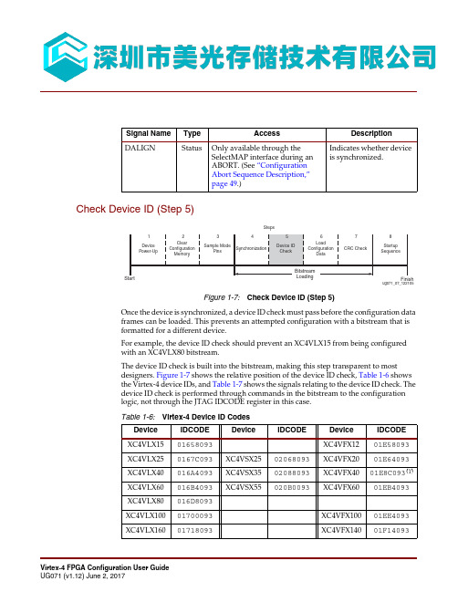
Check Device ID (Step 5)Once the device is synchronized, a device ID check must pass before the configuration data frames can be loaded. This prevents an attempted configuration with a bitstream that is formatted for a different device.For example, the device ID check should prevent an XC4VLX15 from being configured with an XC4VLX80 bitstream.The device ID check is built into the bitstream, making this step transparent to most designers. Figure 1-7 shows the relative position of the device ID check, Table 1-6 shows the Virtex-4 device IDs, and Table 1-7 shows the signals relating to the device ID check. The device ID check is performed through commands in the bitstream to the configuration logic, not through the JTAG IDCODE register in this case.Signal Name Type AccessDescription DALIGNStatusOnly available through the SelectMAP interface during an ABORT. (See “Configuration Abort Sequence Description,” page 49.)Indicates whether device is synchronized.Figure 1-7:Check Device ID (Step 5)Table 1-6:Virtex-4 Device ID CodesDevice IDCODE DeviceIDCODEDevice IDCODE XC4VLX1501658093XC4VFX1201E58093XC4VLX250167C093XC4VSX2502068093XC4VFX2001E64093XC4VLX40016A4093XC4VSX3502088093XC4VFX4001E8C093(1)XC4VLX60016B4093XC4VSX55020B0093XC4VFX6001EB4093XC4VLX80016D8093XC4VLX10001700093XC4VFX10001EE4093XC4VLX16001718093XC4VFX14001F14093Serial Configuration InterfaceClocking Serial Configuration DataFigure2-2 shows how configuration data are clocked into Virtex-4 devices in Slave serialand Master serial modes.Figure 2-2:Serial Daisy Chain Configuration Clocking Sequence Notes relevant to Figure2-2:1.In Figure2-2, bit 0 represents the MSB of the first byte. For example, if the first byte is0xAA (1010_1010), bit 0=1, bit 1=0, bit 2=1, etc.2.For Master configuration mode, CCLK does not transition until after MODE pins aresampled, as indicated by the arrow.LK can be free-running in Slave serial mode.Master Serial ConfigurationThe Master serial mode is designed so that the FPGA can be configured from aXilinx®serial configuration PROM, as shown in Figure2-3.Figure 2-3:Master Serial Mode ConfigurationChapter 2:Configuration InterfacesSlave Serial ConfigurationSlave serial configuration is typically used for devices in a serial daisy chain, or whenconfiguring a single device from an external microprocessor or CPLD. Designconsiderations are similar to Master serial configuration except for the direction of CCLK.A single device in Slave serial mode cannot simply be connected to a PROM, becauseCCLK is an input on both devices.Serial Daisy ChainsMultiple Virtex-4 devices can be configured from a single configuration source byarranging the devices in a serial daisy chain. In a serial daisy chain, devices receive theirconfiguration data through their DIN pin, passing configuration data along todownstream devices through their DOUT pin. The device closest to the configuration datasource is considered the most upstream device, while the device furthest from theconfiguration data source is considered the most downstream device.In a serial daisy chain, the configuration clock is typically provided by the most upstreamdevice in Master serial mode. All other devices are set for Slave serial mode. Figure2-4illustrates this configuration.Alternatively, if a CPLD or microprocessor is used as a configuration controller, all devicescan be set for Slave serial mode. (See “Configuring a Serial Daisy Chain with aMicroprocessor or CPLD,” page 32.)Table 2-4:Virtex-4 SelectMAP Configuration Interface PinsPin NameTypeDedicated or Dual-PurposeDescriptionM[2:0]Input Dedicated MODE pins - determines configuration mode CCLKInput and OutputDedicatedConfiguration clock source for all configuration modes except JTAGSelectMAP Data Three-State Bidirectional Dual PurposeByte-wide (SelectMAP 8 bit) configuration and readback data bus, clocked on rising edge ofCCLK. D0 is the most-significant bit (MSB), D7 the least-significant bit (LSB). In SelectMAP 32 bit, configuring the data order is straight D0=LSB and D31=MSB.(1)Table 2-5:ABORT Status WordBit Number Status Bit Name MeaningD7CFGERR_B Configuration error (active Low)0 = A configuration error has occurred.1 = No configuration error.D6DALIGN Sync word received (active High)0 = No sync word received.1 = Sync word received by interface logic.D5RIP Readback in progress (active High)0 = No readback in progress.1 = A readback is in progress.D4IN_ABORT_B ABORT in progress (active Low)0 = Abort is in progress.1 = No abort in progress.D3-D01111。
Digital Clock Managers (DCMs)DCM SummaryThe Virtex®-4 FPGA Digital Clock Managers (DCMs) provide a wide range of powerfulclock management features:•Clock DeskewThe DCM contains a delay-locked loop (DLL) to completely eliminate clockdistribution delays, by deskewing the DCM's output clocks with respect to the inputclock. The DLL contains delay elements (individual small buffers) and control logic.The incoming clock drives a chain of delay elements, thus the output of every delayelement represents a version of the incoming clock delayed at a different point.The control logic contains a phase detector and a delay-line selector. The phasedetector compares the incoming clock signal (CLKIN) against a feedback input(CLKFB) and steers the delay line selector, essentially adding delay to the output ofDCM until the CLKIN and CLKFB coincide.•Frequency SynthesisSeparate outputs provide a doubled frequency (CLK2X and CLK2X180). Anotheroutput, CLKDV, provides a frequency that is a specified fraction of the inputfrequency.Two other outputs, CLKFX and CLKFX180, provide an output frequency derived fromthe input clock by simultaneous frequency division and multiplication. The user canspecify any integer multiplier (M) and divisor (D) within the range specified in theDCM Timing Parameters section of the Virtex-4 Data Sheet. An internal calculatordetermines the appropriate tap selection, to make the output edge coincide with theinput clock whenever mathematically possible. For example, M=9 and D=5,multiply the frequency by 1.8, and the output rising edge is coincident with the inputrising edge after every fifth input period, or after every ninth output period.•Phase ShiftingThe DCM allows coarse and fine-grained phase shifting. The coarse phase shiftinguses the 90°, 180°, and 270° phases of CLK0 to make CLK90, CLK180, and CLK270clock outputs. The 180° phase of CLK2X and CLKFX provide the respective CLK2X180and CLKFX180 clock outputs.There are also four modes of fine-grained phase-shifting; fixed, variable-positive,variable-center, and direct modes. Fine-grained phase shifting allows all DCM outputclocks to be phase-shifted with respect to CLKIN while maintaining the relationshipbetween the coarse phase outputs. With fixed mode, a fixed fraction of phase shift canbe defined during configuration and in multiples of the clock period divided by 256.Using the variable-positive and variable-center modes the phase can be dynamicallyand repetitively moved forward and backwards by 1/256 of the clock period. With theDCM_BASE PrimitiveThe DCM_BASE primitive accesses the basic frequently used DCM features and simplifiesthe user-interface ports. The clock deskew, frequency synthesis, and fixed-phase shiftingfeatures are available to use with DCM_BASE. Table2-2 lists the available ports in theDCM_BASE primitive.Table 2-2:DCM_BASE PrimitiveAvailable Ports Port NamesClock Input CLKIN, CLKFBControl and Data Input RSTClock Output CLK0, CLK90, CLK180, CLK270, CLK2X, CLK2X180, CLKDV,CLKFX, CLKFX180Status and Data Output LOCKEDDCM_PS PrimitiveThe DCM_PS primitive accesses all DCM features and ports available in DCM_BASE plusadditional ports used by the variable phase shifting feature. DCM_PS also has thefollowing available DCM features: clock deskew, frequency synthesis, and fixed orvariable phase-shifting. Table2-3 lists the available ports in the DCM_PS primitive.Table 2-3:DCM_PS PrimitiveAvailable Ports Port NamesClock Input CLKIN, CLKFB, PSCLKControl and Data Input RST, PSINCDEC, PSENClock Output CLK0, CLK90, CLK180, CLK270, CLK2X, CLK2X180, CLKDV,CLKFX, CLKFX180Status and Data Output LOCKED, PSDONE, DO[15:0]DCM_ADV PrimitiveThe DCM_ADV primitive has access to all DCM features and ports available in DCM_PSplus additional ports for the dynamic reconfiguration feature. It is a superset of the othertwo DCM primitives. DCM_ADV uses all the DCM features including clock deskew,frequency synthesis, fixed or variable phase shifting, and dynamic reconfiguration.Table2-4 lists the available ports in the DCM_ADV primitive.Table 2-4:DCM_ADV PrimitiveAvailable Ports Port NamesClock Input CLKIN, CLKFB, PSCLK, DCLKControl and Data Input RST, PSINCDEC, PSEN, DADDR[6:0], DI[15:0], DWE, DENClock Output CLK0, CLK90, CLK180, CLK270, CLK2X, CLK2X180, CLKDV,CLKFX, CLKFX180Status and Data Output LOCKED, PSDONE, DO[15:0], DRDY1.IBUFG – Global Clock Input BufferThis is the preferred source for an external feedback configuration. When an IBUFG drives a CLKFB pin of a DCM in the same top or bottom half of the device, the pad to DCM skew is compensated for deskew.2.BUFGCTRL – Internal Global Clock BufferThis is an internal feedback configuration.3.IBUF – Input BufferThis is an external feedback configuration. When IBUF is used, the PAD to DCM input skew is not compensated.DCM PortsControl and Data Input PortsReset Input — RSTThe reset (RST) input pin resets the DCM circuitry. The RST signal is an active Highasynchronous reset. Asserting the RST signal asynchronously forces all DCM outputs Low(the LOCKED signal, all status signals, and all output clocks) after some propagation delay.When the reset is asserted, the last cycle of the clocks can exhibit a short pulse and aseverely distorted duty-cycle, or no longer be deskewed with respect to one another whiledeasserting Low. Deasserting the RST signal starts the locking process at the next CLKINcycle.To ensure a proper DCM reset and locking process, the RST signal must be held until theCLKIN and CLKFB signals are present and stable for at least 200ms. (The 200msrequirement for CLKFB only applies when external feedback is used.)The time it takes for the DCM to lock after a reset is specified in the Virtex-4 Data Sheet asLOCK_DLL (for a DLL output) and LOCK_FX (for a DFS output). These are the CLK andCLKFX outputs described in “Clock Output Ports”. The DCM locks faster at higherfrequencies. The worse-case numbers are specified in the Virtex-4 Data Sheet. In all designs,the DCM must be held in reset until CLKIN is stable.Phase-Shift Increment/Decrement Input — PSINCDECThe phase-shift increment/decrement (PSINCDEC) input signal must be synchronouswith PSCLK. The PSINCDEC input signal is used to increment or decrement the phase-shift factor when PSEN is activated. As a result, the output clocks are shifted. ThePSINCDEC signal is asserted High for increment or deasserted Low for decrement. Thisinput must be tied to ground when the CLKOUT_PHASE_SHIFT attribute is set to NONEor FIXED.Phase-Shift Enable Input — PSENChapter 2:Digital Clock Managers (DCMs)Dynamic Reconfiguration Write Enable Input — DWEThe dynamic reconfiguration write enable (DWE) input pin provides the write enablecontrol signal to write the DI data into the DADDR address. When not used, it must be tiedLow. See the Dynamic Reconfiguration chapter of the Virtex-4 Configuration Guide for moreinformation.Dynamic Reconfiguration Enable Input — DENThe dynamic reconfiguration enable (DEN) input pin provides the enable control signal toaccess the dynamic reconfiguration feature. When the dynamic reconfiguration feature isnot used, DEN must be tied Low. When DEN is tied Low, DO reflects the DCM statussignals. See the Dynamic Reconfiguration chapter of the Virtex-4 Configuration Guide formore information.。

Output Delay MeasurementsOutput delays are measured using a T ektronix P6245TDS500/600 probe (<1pF) across approximately 4 inches of FR4 microstrip trace. Standard termination was used for all testing. The propagation delay of the 4 inch trace is char-acterized separately and subtracted from the final measure-ment, and is therefore not included in the generalized test setup shown in Figure 4.Measurements and test conditions are reflected in the IBIS models except where the IBIS format precludes it. Parame-ters V REF , R REF , C REF , and V MEAS fully describe the test conditions for each I/O standard. The most accurate predic-tion of propagation delay in any given application can be obtained through IBIS simulation, using the following method:1.Simulate the output driver of choice into the generalizedtest setup, using values from T able 31.2.Record the time to V MEAS .3.Simulate the output driver of choice into the actual PCBtrace and load, using the appropriate IBIS model or capacitance value to represent the load.4.Record the time to V MEAS .pare the results of steps 2 and 4. The increase ordecrease in delay yields the actual worst-casepropagation delay (clock-to-input) of the PCB trace.DescriptionI/O Standard AttributeR REF (Ω)C REF (1)(pF)V MEAS(V)V REF (V)LVTTL (Low-Voltage T ransistor-T ransistor Logic)LVTTL (all)1M 0 1.40LVCMOS (Low-Voltage CMOS), 3.3V LVCMOS331M 0 1.650LVCMOS, 2.5V LVCMOS251M 0 1.250LVCMOS, 1.8V LVCMOS181M 00.90LVCMOS, 1.5V LVCMOS151M 00.750LVCMOS, 1.2VLVCMOS121M 00.750PCI (Peripheral Component Interface), 33 MHz, 3.3V PCI33_3 (rising edge)2510(2)0.940PCI33_3 (falling edge)2510(2) 2.03 3.3PCI, 66 MHz, 3.3V PCI66_3 (rising edge)2510(2)0.940PCI66_3 (falling edge)2510(2) 2.03 3.3PCI-X, 133 MHz, 3.3VPCIX (rising edge)2510(3)0.94PCIX (falling edge 2510(3) 2.03 3.3GTL (Gunning T ransceiver Logic)GTL 2500.8 1.2GTL PlusGTLP 250 1.0 1.5HSTL (High-Speed Transceiver Logic), Class I HSTL_I 500V REF 0.75HSTL, Class II HSTL_II 250V REF 0.75HSTL, Class III HSTL_III 5000.9 1.5HSTL, Class IV HSTL_IV 2500.9 1.5HSTL, Class I, 1.8V HSTL_I_18500V REF 0.9HSTL, Class II, 1.8V HSTL_II_1825V REF0.9HSTL, Class III, 1.8VHSTL_III_18500 1.1 1.8CLB Switching Characteristics Table 37: CLB Switching CharacteristicsSymbol DescriptionSpeed GradeUnits -12-11-10XC4VFX(2)XC4VLX/SX ALL DEVICESCombinatorial DelaysT ILO4-input function: F/G inputs to X/Y outputs0.150.150.170.20ns, Max T IF55-input function: F/G inputs to F5 output0.360.350.400.46ns, Max T IF5X5-input function: F/G inputs to X output0.440.430.490.57ns, Max T IF6Y FXINA or FXINB inputs to YMUX output0.300.300.340.39ns, Max T INAFX FXINA input to FX output via MUXFX0.210.210.230.27ns, Max T INBFX FXINB input to FX output via MUXFX0.210.200.230.26ns, Max T BXX BX input to XMUX output0.590.580.650.76ns, Max T BYY BY input to YMUX output0.430.430.480.56ns, Max T BXCY BX input to C OUT output – Getting into carry chain(3)0.600.590.660.78ns, Max T BYCY BY input to C OUT output – Getting into carry chain(3)0.490.480.540.63ns, Max T BYP C IN input to C OUT output – Carry chain delay(3)0.070.070.080.09ns, Max T OPCYF F input to C OUT output – Getting out from carry chain(3)0.450.440.500.58ns, Max T OPCYG G input to C OUT output – Getting out from carry chain(3)0.440.430.480.57ns, Max Sequential DelaysT CKO FF Clock CLK to XQ/YQ outputs0.280.280.310.36ns, Max T CKLO Latch Clock CLK to XQ/YQ outputs0.370.360.410.48ns, Max Setup and Hold Times of CLB Flip-Flops Before/After Clock CLKT DICK/T CKDIBX/BY inputs0.36–0.090.36–0.090.40–0.090.47–0.09ns, MinT CECK/T CKCECE input0.58–0.160.57–0.160.64–0.160.75–0.16ns, MinT FXCK/T CKFXFXINA/FXINB inputs0.42–0.140.41–0.140.46–0.140.54–0.14ns, MinT SRCK/T CKSRSR/BY inputs (synchronous)1.04–0.741.02–0.731.15–0.731.35–0.73ns, MinT CINCK/T CKCINC IN Data Inputs (DI) – Getting out from carry chain(3)0.52–0.230.51–0.230.57–0.230.67–0.23ns, MinSet/ResetT RPW Minimum Pulse Width, SR/BY inputs0.540.530.590.70ns, Min T RQ Delay from SR/BY inputs to XQ/YQ outputs(asynchronous)1.05 1.03 1.15 1.35ns, MaxF TOG Toggle Frequency (MHz) (for export control)118112051205(4)1028MHz Notes:1. A Zero “0” Hold Time listing indicates no hold time or a negative hold time. Negative values cannot be guaranteed “best-case,” but if a “0” is listed,there is no positive hold time.2.The values in this column apply to all XC4VFX -12 parts except XC4VFX12 -12. For XC4VFX12 -12 values, use the values in the adjacent 4VLX/SX-12 column.3.These items are of interest for Carry Chain applications.4.XC4VFX -11 devices are 1181MHz.CLB Distributed RAM Switching Characteristics (SLICEM Only)Table 38: CLB Distributed RAM Switching CharacteristicsSymbolDescription Speed Grade Units-12-11-10XC4VFX (2)XC4VLX/SX ALL DEVICESSequential Delays T SHCKO Clock CLK to X outputs (WE active)(3) 1.61 1.58 1.77 2.08ns, Max T SHCKOF5Clock CLK to F5 output (WE active)1.53 1.50 1.69 1.98ns, MaxSetup and Hold Times Before/After Clock CLK T DS /T DH BX/BY data inputs (DI) 1.26–0.90 1.23–0.88 1.46–0.88 1.80–0.88ns, Min T AS /T AH F/G address inputs 0.88–0.370.86–0.370.97–0.34 1.13–0.29ns, Min T WS /T WH WE input (SR)1.10–0.48 1.08–0.47 1.21–0.47 1.42–0.47ns, MinClock CLK T WPH Minimum Pulse Width, High 0.530.520.590.69ns, Min T WPL Minimum Pulse Width, Low0.550.540.600.70ns, Min T WCMinimum clock period to meet address write cycle time0.760.740.840.98ns, MinCLKOUT_FREQ_FX_HF_MS_MINCLKFX, CLKFX180210210210MHz CLKOUT_FREQ_FX_HF_MS_MAX 350315300MHzInput Clocks (High Frequency Mode)CLKIN_FREQ_DLL_HF_MS_MIN (6)CLKIN (using DLL outputs only)(1,3,4,5)150150150MHz CLKIN_FREQ_DLL_HF_MS_MAX 500450400MHz CLKIN_FREQ_FX_HF_MS_MIN CLKIN (using DFS outputs)(2,3,4)505050MHz CLKIN_FREQ_FX_HF_MS_MAX (6)350315300MHz PSCLK_FREQ_HF_MS_MIN PSCLK111KHz PSCLK_FREQ_HF_MS_MAX500450400MHzTable 45: Operating Frequency Ranges for DCM in Maximum Speed (MS) Mode (Continued)SymbolDescriptionSpeed GradeUnits-12-11-10Table 47: Input Clock TolerancesSymbolDescriptionFrequency RangeValue UnitsDuty Cycle Input Tolerance (in %)CLKIN_PSCLK_PULSE_RANGE_1PSCLK only< 1MHz 25-75%CLKIN_PSCLK_PULSE_RANGE_1_50PSCLK and CLKIN 1 – 50MHz (1)25-75%CLKIN_PSCLK_PULSE_RANGE_50_10050 – 100MHz (1)30-70%CLKIN_PSCLK_PULSE_RANGE_100_200100 – 200MHz (1)40-60%CLKIN_PSCLK_PULSE_RANGE_200_400200 – 400MHz (1)45-55%CLKIN_PSCLK_PULSE_RANGE_400>400MHz45-55%。
Thermal SpecificationsSummaryThis chapter provides thermal data associated with Virtex-4 FPGA packages. Thefollowing topics are discussed:∙Introduction∙Virtex-4 FPGA Power Management Strategy∙Some Thermal Management Options∙Support for Compact Thermal Models (CTM)∙ReferencesIntroductionVirtex-4 devices are offered exclusively in thermally efficient flip-chip BGA packages. ThisFPGA family’s three product lines have different thermal needs. The LX devices are thebase family members, with traditional Virtex-II FPGA features implemented in the smallerprocess technology. The FX and SX family members take system integration a few stepsfurther, with the incorporation of embedded circuits on top of the base FPGA fabric.Similar to Virtex-II FPGAs, all Virtex-4 family members feature versatile SelectIO resourcesthat support a variety of I/O standards, on-board digitally controlled impedance (DCI),and many other popular features contained in earlier Virtex FPGA products. In addition,the FX family incorporates faster RocketIO multi-gigabit transceivers (MGTs) and one ormore embedded PowerPC devices. The SX devices include an embedded DSP. The extentof system integration in a fully configured design that is exploiting the fabric and usingseveral embedded circuits and systems (such as PowerPC devices, MGTs, SelectIO buseswith DCI, and so forth) presents a power consumption challenge that must be managed.Unlike features in an ASIC or a microprocessor, the combination of FPGA features utilizedin an end-user application will not be known to the component supplier. Therefore, itremains a challenge for Xilinx to predict the power requirements of a given Virtex-4 devicewhen it leaves the factory. Accurate estimates are obtained when the board design takesshape. For this purpose, Xilinx offers and supports a suite of integrated device poweranalysis tools to help end-users quickly and accurately estimate their design powerrequirements. The uncertainty of design power requirements makes it difficult to applycanned thermal solutions to fit all users. Therefore, Xilinx® devices do not come withpreset thermal solutions. The end user’s operating conditions dictate the appropriatesolution.The Virtex-4 FPGA package offering (see Table 5-1) is tailored to include medium to high-power options that allow external management of power to suit the user application.Table 5-1 also shows the thermal resistance data for Virtex-4 devices in the packagesChapter 5: Thermal Specifications Table 5-1: Thermal Resistance DataPackage Device Package Body SizeθJCθJB θJA @0 LFMθJA @250 LFMθJA @500 LFMθJA @750 LFMLX and SX DevicesSF363LX1517.00.5 5.620.814.712.912.0 LX2517.00.3 4.919.013.511.811.0 FF668LX1527.00.6 4.414.29.37.87.1 LX2527.00.4 4.013.48.77.3 6.7LX4027.00.3 3.613.08.57.1 6.5LX6027.00.2 3.412.48.1 6.8 6.2SX2527.00.4 3.913.48.77.3 6.7SX3527.00.2 3.612.78.37.0 6.4 FF676LX1527.00.6 4.414.29.37.87.1 LX2527.00.4 4.013.48.77.3 6.7 FF1148LX4035.00.3 2.811.0 6.7 5.5 4.9 LX6035.00.2 2.610.6 6.4 5.3 4.8LX8035.00.2 2.410.4 6.3 5.1 4.6LX10035.00.1 2.210.1 6.1 5.0 4.5LX16035.00.1 2.19.7 5.9 4.8 4.3SX5535.00.2 2.410.3 6.3 5.1 4.6 FF1513LX10040.00.1 2.39.7 5.8 4.7 4.2 LX16040.00.1 2.29.3 5.6 4.5 4.0LX20040.00.1 2.09.1 5.5 4.4 4.0 FX DevicesSF363FX1217.00.5 5.720.814.712.912.0 FF668FX1227.00.6 4.414.29.37.87.1 FF672FX2027.00.4 3.813.58.77.4 6.8 FX4027.00.2 3.312.68.2 6.9 6.3FX6027.00.1 3.112.07.7 6.5 5.9 FF1152FX4035.00.2 2.610.7 6.5 5.3 4.8 FX6035.00.2 2.510.2 6.2 5.1 4.7FX10035.00.1 2.29.9 6.0 4.9 4.4 FF1517FX10040.00.1 2.29.5 5.7 4.6 4.1 FX14040.00.1 2.08.6 5.0 4.1 3.7Virtex-4 FPGA Power Management StrategyVirtex-4 FPGA Power Management StrategyXilinx relies on a multi-prong approach with regards to the heat-dissipating potential ofVirtex-4 devices:Chapter 5: Thermal SpecificationsSome Thermal Management OptionsThe flip-chip thermal management chart in Figure 5-2 illustrates simple but incrementalpower management schemes that can be applied on a flip-chip BGA package.Support for Compact Thermal Models (CTM) bulky heat sink is attached. The thermal interface resistance needs to be controlled totake full advantage of these packages.∙An active heat sink may include a simple heat sink incorporating a mini fan or even a Peltier Thermoelectric Cooler (TEC) with a fan to carry away any dissipated heat.When considering the use of a TEC for heat management, consultation with experts in using the device is important because these devices can be reversed and causedamage to components. Also condensation can be an issue with these devices.∙Outside the package itself, the board on which the package sits can have a significant impact on thermal performance. As much as 60 to 80% of the dissipated heat can go through the BGA balls and thus to the board. Using the standard four-layer JEDEC boards, these with their multiple internal vias show very efficient junction-to-board resistances. Designs can be implemented to take advantage of the board's ability to spread heat. The effect of the board is dependent on its size and how it conducts heat.Board size, the level of copper traces on it, the number of buried copper planes all lower the junction-to-ambient thermal resistance for a package mounted on it. The cold ring junction-to-board thermal resistance for Virtex-4 FPGA packages are given in Table 5-1.。
Chapter1 KCU105 Evaluation Board FeaturesOverviewThe KCU105 evaluation board for the Xilinx® Kintex® UltraScale™ FPGA provides a hardware environment for developing and evaluating designs targeting the UltraScaleXCKU040-2FFVA1156E device. The KCU105 evaluation board provides features common to many evaluation systems, including a DDR4 component memory, a high definitionmultimedia interface (HDMI™), two small form-factor pluggable (SFP+) connectors, aneight-lane PCI Express® interface, an Ethernet PHY, general purpose I/O, and two UARTinterfaces. Other features can be added by using VITA-57 FPGA mezzanine cards (FMCs) attached to the low pin count (LPC) FMC and high pin count (HPC) FMC connectors.KCU105 Evaluation Board FeaturesThe KCU105 evaluation board features are listed here. Detailed information for each feature is provided in Feature Descriptions.•Kintex UltraScale XCKU040-2FFVA1156E device•Zynq® SoC XC7Z010 based system controller•2GB DDR4 component memory (four [256Mb x16] devices)•Dual 256Mb Quad serial peripheral interface flash memory (Dual Quad SPI)•Micro secure digital (SD) connector•USB JTAG interface via Digilent module with micro-B USB connector•Clock sources:°Si5335A quad fixed frequency clock generator (300MHz, 125MHz, 90MHz,33.333MHz)°Si5328B clock multiplier and jitter attenuator (8kHz - 808MHz)°Si570 I2C programmable LVDS clock generator (10MHz - 810MHz)°Subminiature version A (SMA) connectors (differential)•20 GTH transceivers (five Quads)°FMC HPC connector (eight GTH transceivers)The KCU105 board DDR4 memory component interface adheres to the constraintsguidelines documented in the DDR4 Design Guidelines section of UltraScale Architecture PCB Design User Guide (UG583) [Ref 3] and in UltraScale Architecture-Based FPGAs Memory IP LogiCORE IP Product Guide (Vivado Design Suite) (PG150) [Ref 4]. The KCU105 board DDR4 memory component interface is a 40Ω impedance implementation. For more details about the Micron DDR4 component memory, see the Micron EDY4016AABG-DR-F-D data sheet at the Micron website [Ref 5].Dual Quad-SPI Flash Memory[Figure 1-2, callout 3]The Quad-SPI flash memory located at U35 and U36 provides 2 x 256Mb of nonvolatile storage that can be used for configuration and data storage. For details on FPGAconfiguration operation and implementation related to the dual Quad-SPI interfaces, see UltraScale Architecture Configuration User Guide (UG570) [Ref 2].•Part number: N25Q256A11ESF40F (Micron)•Supply voltage: 1.8VAG19DDR4_A13SSTL12_DCI T8A13U60-U62AD16DDR4_A14_WE_B SSTL12_DCI L2WE_B/A14U60-U62AG14DDR4_A15_CAS_B SSTL12_DCI M8CAS_B/A15U60-U62AF14DDR4_A16_RAS_BSSTL12_DCI L8RAS_B/A16U60-U62AF17DDR4_BA0SSTL12_DCI N2BA0U60-U62AL15DDR4_BA1SSTL12_DCI N8BA1U60-U62AG15DDR4_BG0SSTL12_DCI M2BG0U60-U62AH14DDR4_ACT_B SSTL12_DCI L3ACT_B U60-U62AH16DDR4_TEN SSTL12_DCI N9TEN U60-U62AJ16DDR4_ALERT_B SSTL12_DCI P9ALERT_B U60-U62AD18DDR4_PAR SSTL12_DCI T3PAR U60-U62AJ18DDR4_ODT SSTL12_DCI K3ODT U60-U62AL19DDR4_CS_B SSTL12_DCI L7CS_B U60-U62AD15DDR4_CKE SSTL12_DCI K2CKE U60-U62AL18DDR4_RESET_B LVCMOS12P1RESET_B U60-U62AE16DDR4_CK_T DIFF_SSTL12_DCI K7CK_T U60-U62AE15DDR4_CK_CDIFF_SSTL12_DCIK8CK_CU60-U62Table 1-4:DDR4 Memory Connections to the FPGA (Cont’d)FPGA (U1) PinSchematic NetNameI/O StandardComponent MemoryPin #Pin NameRef. Des.FPGA (U1)Pin Schematic NetName I/O Standard Pin # Pin Name Ref. Des.AC7QSPI0_IO0LVCMOS1815SI_IO0U35 AB7QSPI0_IO1LVCMOS188SI_IO1U35 AA7QSPI0_IO2LVCMOS189SI_IO2U35 Y7QSPI0_IO3LVCMOS181SI_IO3U35 AA9FPGA_CCLK NA(1)16SCK U35, U36Table 1-13 lists the SFP+ module connections to FPGA U1.Table 1-13:KCU105 Board FPGA U1 to SFP0 and SFP1 Module Connections FPGA (U1)PinSchematic Net NameFPGA (U1) Direction Pin NumberPin NameSFP/SFP+ ModuleT2SFP0_RX_P Input 13RD_P SFP0 P5T1SFP0_RX_N Input 12RD_N U4SFP0_TX_P Output 18TD_P U3SFP0_TX_N Output 19TD_N AL8SFP0_TX_DISABLEOutput 3TX_DISABLEV2SFP1_RX_P Input 13RD_P SFP1 P4V1SFP1_RX_N Input 12RD_N W4SFP1_TX_P Output 18TD_P W3SFP1_TX_N Output 19TD_N D28SFP1_TX_DISABLEOutput3TX_DISABLEIIC_MUX_RESET_B_LS must be driven High to enable I2C bus transactions with the devices connected to U28.User FPGA applications that communicate with devices on one of the downstream I2C buses must first set up a path to the desired target bus through the U28 or U80 bus switch at I2C address 0x74 (0b1110100) or 0x75 (0b1110101), respectively. Table1-19 lists the address for each device on the I2C bus.。
RocketIO GTX Transceiver User GuideUG198 (v3.0) October 30, 2009Shared PMA PLLPorts and AttributesTable 5-1 defines the shared PMA PLL ports.Table 5-2 defines the shared PMA PLL attributes.Table 5-1:Shared PMA PLL Ports Port DirDomain Description CLKIN In Async Reference clock input to the shared PMA PLL. See “Clocking,” page 96 formore information about the different ways this port can be driven.INTDATAWIDTH In Async Sets the internal datapath width for the GTX_DUAL tile. If Low, the internaldatapath width is set to 16 bits. If High, the internal datapath width is set to20 bits.PLLLKDET Out Async This port indicates that the VCO rate is within acceptable tolerances of thedesired rate when High. Neither GTX transceiver in the tile operates reliablyuntil this condition is met.PLLLKDETEN In Async This port enables the PLL lock detector and must always be tied High.REFCLKOUT Out AsyncThe REFCLKOUT port from each GTX_DUAL tile provides direct access tothe reference clock provided to the shared PMA PLL (CLKIN). It can berouted for use in the FPGA logic.Table 5-2:Shared PMA PLL Attributes Attribute Type DescriptionOVERSAMPLE_MODE Boolean When OVERSAMPLE_MODE is TRUE, then DIV =5 regardless of the settingof INTDATAWIDTH.When OVERSAMPLE_MODE is FALSE, andINTDATAWIDTH is Low, then DIV =4 orINTDATAWIDTH is High, then DIV =5PLL_DIVSEL_FB Integer Controls the feedback divider. Valid settings for PLL_DIVSEL_FB are 1, 2, 3, 4,and 5. PLL_DIVSEL_FB is multiplied by 4 or 5, depending on the width of theinternal datapath as set by INTDATAWIDTH. If INTDATAWIDTH is Low, thefeedback divider N is set to PLL_DIVSEL_FB x 4. If INTDATAWIDTH is High,the feedback divider N is set to PLL_DIVSEL_FB x 5.PLL_DIVSEL_REF Integer Controls the reference clock divider. Valid settings for PLL_DIVSEL_REF are 1and 2.PLL_RXDIVSEL_OUT_0PLL_RXDIVSEL_OUT_1Integer Divides the PLL clock to produce a high-speed RX clock. Because both edgesof the clock are used, the divided clock must run at one-half the desired RX linerate. Permitted divider settings are 1, 2, and 4. See “Serial In to Parallel Out,”page 183 for details.PLL_TXDIVSEL_OUT_0PLL_TXDIVSEL_OUT_1IntegerDivides the PLL clock to produce a high-speed TX clock. Because both edges ofthe clock are used, the divided clock must run at one-half the desired TX linerate. Divider settings are 1, 2, and 4. Each GTX transceiver has its ownPLL_TXDIVSEL_OUT. See “Parallel In to Serial Out,” page 149 for details.RocketIO GTX Transceiver User Guide UG198 (v3.0) October 30, 2009Chapter 1:Introduction to the RocketIO GTX TransceiverChapter 5:Tile FeaturesDescriptionThe GTX_DUAL tile offers different levels of power control. Each channel in each directioncan be powered down separately using TXPOWERDOWN and RXPOWERDOWN.Additionally, the part of the reference clock circuit between the differential clock input pairpin and dedicated clock routing circuit can be powered down. The PLLPOWERDOWNport directly affects the shared PMA PLL and therefore both channels of the GTX_DUALtile.Generic GTX Power-Down CapabilitiesThe GTX_DUAL tile provides several power-down features that can be used in a widevariety of applications. Table5-12 summarizes these capabilities.Table 5-12:Basic Power-Down Functions SummaryFunction Controlled By AffectsREFCLK Power Down REFCLKPWRDNB The GTX_DUAL tile (TX and RX forboth transceivers) when using anexternal oscillator to drive thededicated clock routing, and alldownstream GTX_DUAL tiles sharingthat REFCLK.PLL Power Down PLLPOWERDOWN TX and RX for both transceivers in aGTX_DUAL tile. Powers down theshared PMA PLL as well as the RX andTX PMA circuits.TX Power Down TXPOWERDOWN[1:0]TX in a single transceiver.RX Power Down RXPOWERDOWN[1:0]RX in a single transceiver.REFCLK Power DownTo activate the REFCLK power-down mode, the active-Low REFCLKPWRDNB signal isasserted. When REFCLKPWRDNB is asserted, toggling of all circuitry between thedifferential clock pair input pins and the dedicated clock routing circuitry is suppressed.As long as power is applied to a GTX_DUAL tile, all other circuitry including thededicated clock routing and shared PMA PLL continue to toggle even whenREFCLKPWRDNB is asserted. This is a different implementation from the GTP_DUAL tilewhere when REFCLKPWRDNB is asserted, the dedicated clocking routing circuity isdisabled and all circuitry clocked by the REFCLK input is suppressed, including the sharedPMA PLL and all clocks derived from it. If the GTX_DUAL tiles share a common reference,REFCLK is suppressed to tiles that are downstream in the clock routing chain. Figure5-3,page97 illustrates how the dedicated clock routing blocks forward REFCLKs betweenGTX_DUAL tiles.Deactivation of the REFCLK power-down mode is indicated by the PLLLKDET signal,which is asserted on the tiles sourcing the affected reference clocks.PLL Power DownTo activate the PLL power-down mode, the active-High PLLPOWERDOWN signal isasserted. When PLLPOWERDOWN is asserted, the shared PMA PLL and both the PMATX and PMA RX circuits are powered down. As a result, all clocks derived from the PMAPLL are stopped. This is a different implementation than for the GTP_DUAL tile whereRocketIO GTX Transceiver User GuideUG198 (v3.0) October 30, 2009。
Virtex-4 FPGA Electrical CharacteristicsVirtex®-4 FPGAs are available in -12, -11, and -10 speed grades, with -12 having the highest performance.Virtex-4 FPGA DC and AC characteristics are specified for both commercial and industrial grades. Except the operat-ing temperature range or unless otherwise noted, all the DC and AC electrical parameters are the same for a particular speed grade (that is, the timing characteristics of a -10speed grade industrial device are the same as for a -10speed grade commercial device). However, only selected speed grades and/or devices might be available in the industrial range.All supply voltage and junction temperature specifications are representative of worst-case conditions. The parame-ters included are common to popular designs and typical applications.This Virtex-4 FPGA Data Sheet is part of an overall set of documentation on the Virtex-4 family of FPGAs that is avail-able on the Xilinx website:•Virtex-4 Family Overview, DS112•Virtex-4 FPGA User Guide, UG070•Virtex-4 FPGA Configuration Guide, UG071•XtremeDSP for Virtex-4 FPGAs User Guide, UG073•Virtex-4 FPGA Packaging and Pinout Specification,UG075•Virtex-4 FPGA PCB Designer’s Guide, UG072•Virtex-4 RocketIO™ Multi-Gigabit T ransceiver User Guide, UG076•Virtex-4 FPGA Embedded T ri-Mode Ethernet MAC User Guide, UG074•PowerPC® 405 Processor Block Reference Guide,UG018All specifications are subject to change without notice.Virtex-4 FPGA DC CharacteristicsDS302 (v3.7) September 9, 2009Product SpecificationTable 1: Absolute Maximum RatingsSymbolDescriptionUnitsV CCINT Internal supply voltage relative to GND –0.5 to 1.32V V CCAUX Auxiliary supply voltage relative to GND –0.5 to 3.0V V CCO Output drivers supply voltage relative to GND –0.5 to 3.75V V BA TT Key memory battery backup supply –0.5 to 4.05V V REFInput reference voltage–0.3 to 3.75V V INI/O input voltage relative to GND (all user and dedicated I/Os)–0.75 to 4.05VI/O input voltage relative to GND(restricted to maximum of 100 user I/Os)(3,4)–0.95 to 4.4(Commercial T emperature)–0.85 to 4.3(Industrial T emperature)V2.5V or below I/O input voltage relative to GND (user and dedicated I/Os)–0.75 to V CCO +0.5V I INCurrent applied to an I/O pin, powered or unpowered ±100mA T otal current applied to all I/O pins, powered or unpowered±200mADescription Symbol ConstraintsSpeed GradeUnits -12-11-10Clock Synthesis Period JitterCLK0CLKOUT_PER_JITT_0±100±100±100ps CLK90CLKOUT_PER_JITT_90±150±150±150ps CLK180CLKOUT_PER_JITT_180±150±150±150ps CLK270CLKOUT_PER_JITT_270±150±150±150ps CLK2X, CLK2X180CLKOUT_PER_JITT_2X±200±200±200ps CLKDV (integer division)CLKOUT_PER_JITT_DV1±150±150±150ps CLKDV (non-integer division)CLKOUT_PER_JITT_DV2±300±300±300ps CLKFX, CLKFX180CLKOUT_PER_JITT_FX Note (2)Note (2)Note (2)psTable 50: Miscellaneous Timing ParametersSymbol DescriptionSpeed GradeUnits -12-11-10Time Required to Achieve LOCKT_LOCK_DLL_240DLL output – Frequency range > 240MHz (2)202020µs T_LOCK_DLL_120_240DLL output – Frequency range 120 - 240MHz (1,2)636363µs T_LOCK_DLL_60_120DLL output – Frequency range 60 - 120MHz (1,2)225225225µs T_LOCK_DLL_50_60DLL output – Frequency range 50 - 60MHz(1,2)325325325µs T_LOCK_DLL_40_50DLL output – Frequency range 40 - 50MHz (1,2)500500500µs T_LOCK_DLL_30_40DLL output – Frequency range 30 - 40MHz (1,2)900900900µs T_LOCK_DLL_24_30DLL output – Frequency range 24 - 30MHz(1,2)125012501250µs T_LOCK_DLL_30DLL output – Frequency range < 30MHz (2)125012501250µs T_LOCK_FX_MAX DFS outputs(3)101010ms T_LOCK_DLL_FINE_SHIFT Multiplication factor for DLL lock time with Fine Shift222Fine Phase ShiftingFINE_SHIFT_RANGE_MS Absolute shifting range in maximum speed mode777ns FINE_SHIFT_RANGE_MR Absolute shifting range in maximum range mode101010ns Delay LinesDCM_T AP_MS_MIN T ap delay resolution (Min) in maximum speed mode555ps DCM_T AP_MS_MAX T ap delay resolution (Max) in maximum speed mode404040ps DCM_T AP_MR_MIN T ap delay resolution (Min) in maximum range mode101010ps DCM_T AP_MR_MAX T ap delay resolution (Max) in maximum range mode606060ps Input Signal RequirementsDCM_RESET(4)Minimum duration that RST must be held asserted200200200ms Maximum duration that RST can be held asserted(5)101010secDCM_INPUT_CLOCK_STOP Maximum duration that CLKIN and CLKFB can bestopped(6,7)100100100msNotes:1.For boundary frequencies, choose the higher delay.2.DLL Outputs are used in these instances to describe the outputs: CLK0, CLK90, CLK180, CLK270, CLK2X, CLK2X180, and CLKDV.3.DFS Outputs are used in these instances to describe the outputs: CLKFX and CLKFX180.4.CLKIN must be present and stable during the DCM_RESET.5.This only applies to production step 1 LX and SX devices. For these devices, use the design solutions described in Answer Record 21127 for supportof longer reset durations. Production step 2 LX and SX devices and all production FX devices do not have this requirement.6.For production step 1 LX and SX devices, use the design solutions described in Answer Record 21127 for support of longer durations of stoppedclocks. For production step 2 LX and SX devices and all production FX devices, the ISE software automatically inserts a small macro to support longer durations of stopped clocks.7.For all stepping levels, once the input clock is toggling again and stable after being stopped, DCM must be reset.Symbol Description DeviceSpeed GradeUnits -12-11-10LVCMOS25 Global Clock Input to Output Delay using Output Flip-Flop, 12mA, Fast Slew Rate, with DCM.T ICKOFDCM Global Clock and OFF with DCM XC4VLX15 2.43 2.81 3.25nsXC4VLX25 2.60 2.95 3.36nsXC4VLX40 2.54 2.91 3.32nsXC4VLX60 2.69 3.05 3.45nsXC4VLX80 2.88 3.27 3.72nsXC4VLX100 2.94 3.33 3.79nsXC4VLX160 2.94 3.35 3.82nsXC4VLX200N/A 3.51 4.02nsXC4VSX25 2.65 2.99 3.39nsXC4VSX35 2.81 3.18 3.60nsXC4VSX55 2.83 3.20 3.62nsXC4VFX12 2.43 2.78 3.18nsXC4VFX20 2.54 2.88 3.26nsXC4VFX40 2.87 3.25 3.67nsXC4VFX60 2.92 3.31 3.77nsXC4VFX100 3.16 3.58 4.06nsXC4VFX140N/A 3.79 4.30nsTable 61: Sample WindowSymbol Description DeviceSpeed GradeUnits -12-11-10T SAMP Sampling Error at Receiver Pins(1)All450500550ps T SAMP_BUFIO Sampling Error at Receiver Pins using BUFIO(2)All350400450psSymbol DescriptionSpeed GradeUnits -12-11-10Data Input Setup and Hold Times Relative to a Forwarded Clock Input Pin Using BUFIOT PSCS/T PHCS Setup/Hold of I/O clock across multiple clock regions –0.450.97–0.451.08–0.441.17nsPin-to-Pin Clock-to-Out Using BUFIOT ICKOFCS Clock-to-Out of I/O clock across multiple clock regions 4.10 4.54 5.02ns。
Device/Package Combinations and Maximum I/Os
Table 1-1 shows the maximum number of user I/Os possible in Virtex-4 FPGA flip-chip packages.∙SF denotes flip-chip fine-pitch BGA (0.80 mm pitch)∙
FF denotes flip-chip fine-pitch BGA (1.00 mm pitch)
Table 1-2 shows the number of available I/Os, the number of RocketIO™ multi-gigabit transceivers (MGTs), and the number of differential I/O pairs for each Virtex-4 XC4VLX, XC4VSX, and XC4VFX device/package combination. The number of I/Os per package includes all user I/Os except the fifteen control pins (CCLK, DONE, M0, M1, M2, PROG_B, PWRDWN_B, TCK, TDI, TDO, TMS, HSWAPEN, DXN, DXP, AND RSVD) and the RocketIO MGT pins (AVCCAUXTX, AVCCAUXRX, AVCCAUXMGT, TXP, TXN, RXP, RXN, VTTX, VTRX, MGTCLK, MGTVREF, RTERM, and GNDA).
Table 1-1: Flip-Chip Packages
Package SF363FF668FF672FF676FF1148FF1152FF1513FF1517Pitch (mm)0.80 mm 1.00 mm 1.00 mm 1.00 mm 1.00 mm 1.00 mm 1.00 mm 1.00 mm Size (mm)17 x 1727 x 2727 x 2727 x 2735 x 3535 x 3540 x 4040 x 40Maximum I/Os
240
448
352
448
768
576
960
768
Table 1-2: Virtex-4 FPGA Available I/Os and RocketIO MGT Pins per Device/Package Combination
Virtex-4
Device
User I/Os & RocketIO MGT Pins Virtex-4 FPGA Package
SF363FF668FF672FF676FF1148
FF1152
FF1513
FF1517
XC4VLX15
Available User I/Os
240320-320----RocketIO Transceivers N/A N/A -N/A ----Differential I/O Pairs 120160-160----XC4VLX25
Available User I/Os
240448-448----RocketIO Transceivers N/A N/A -N/A ----Differential I/O Pairs 120224-224
----XC4VLX40
Available User I/Os
-448-640---RocketIO Transceivers -N/A -N/A ---Differential I/O Pairs -224-320---XC4VLX60
Available User I/Os
-448-640---RocketIO Transceivers -N/A -N/A ---Differential I/O Pairs -224-320---XC4VLX80
Available User I/Os
---768---RocketIO Transceivers ---N/A ---Differential I/O Pairs
---384
---
FF672 Flip-Chip Fine-Pitch BGA Package
10
IO_L17P_10 M10NC 10 IO_L17N_10 M9NC 10 IO_L18P_10 N8NC 10 IO_L18N_10 N7NC 10 IO_L19P_10 M11NC 10 IO_L19N_10 N11NC 10 IO_L20P_10 P8NC 10 IO_L20N_VREF_10
R8NC 10 IO_L21P_10 P11NC 10 IO_L21N_10 P10NC 10 IO_L22P_10 P6NC 10 IO_L22N_10 N6NC 10 IO_L23P_VRN_10 N9NC 10 IO_L23N_VRP_10 P9NC 10 IO_L24P_CC_LC_10 R7NC 10
IO_L24N_CC_LC_10
R6
NC
Table 2-3: FF672 Package — FX60, FX40, and FX20 Devices (Continued)Bank
Pin Description
Pin Number
No Connects in FX20 Devices
Chapter 2: Pinout Tables
FF676 Flip-Chip Fine-Pitch BGA Package
As shown in Table 2-4, Virtex-4 XC4VLX15 and XC4VLX25 devices are available in the
FF676 flip-chip fine-pitch BGA package.
The “No Connect” column in Table 2-4 shows pins that are not available in LX15 devices.
To be assured of having the very latest Virtex-4 FPGA pinout information, visit
and check for any updates to this document. ASCII package pinout files are also
available for download from the Xilinx website.
Table 2-4: FF676 Package — LX15 and LX25 Devices
Bank Pin Description Pin Number No Connects in LX15 Devices
0 HSWAPEN_0 K16 0 CCLK_0 M14 0 D_IN_0 L13 0 PROG_B_0 K17 0 INIT_B_0 K15 0 CS_B_0 M12 0DONE_0L15 0 RDWR_B_0 R11 0 VBATT_0 L17 0 M2_0 M16 0 PWRDWN_B_0 U12 0TMS_0T10 0 M0_0 P14 0TDO_0R13 0TCK_0U10 0 M1_0 R15 0 DOUT_BUSY_0 T14 0TDI_0U11 0TDN_0F12 0TDP_0E12
1 IO_L1P_D31_LC_1 J14 1 IO_L1N_D30_LC_1 H14 1 IO_L2P_D29_LC_1 J13 1 IO_L2N_D28_LC_1 H13 1 IO_L3P_D27_LC_1 J16 1 IO_L3N_D26_LC_1 J15 1 IO_L4P_D25_LC_1 K13 1 IO_L4N_D24_VREF_LC_1 K1
2 1 IO_L5P_D23_LC_1 G15
FF676 Flip-Chip Fine-Pitch BGA Package
1
IO_L5N_D22_LC_1 G141 IO_L6P_D21_LC_1 H121 IO_L6N_D20_LC_1 H111 IO_L7P_D19_LC_1 H161 IO_L7N_D18_LC_1 G161 IO_L8P_D17_CC_LC_1 J111
IO_L8N_D16_CC_LC_1
K11
Table 2-4: FF676 Package — LX15 and LX25 Devices (Continued)Bank
Pin Description
Pin Number
No Connects in LX15 Devices
Chapter 2: Pinout Tables
3 IO_L7P_GC_LC_3 F153 IO_L7N_GC_LC_3 F14
3 IO_L8P_GC_LC_3 A133
IO_L8N_GC_LC_3
A12
4 IO_L1P_GC_LC_4 AA144 IO_L1N_GC_LC_4 AA134 IO_L2P_GC_LC_4 AB124 IO_L2N_GC_LC_4 AA124
IO_L3P_GC_LC_4
AB14
Table 2-4: FF676 Package — LX15 and LX25 Devices (Continued)Bank
Pin Description
Pin Number
No Connects in LX15 Devices。